Sign In
Upload
Manuals
Brands
ST Manuals
Motherboard
STM32H7B3I-EVAL
ST STM32H7B3I-EVAL Manuals
Manuals and User Guides for ST STM32H7B3I-EVAL. We have
1
ST STM32H7B3I-EVAL manual available for free PDF download: User Manual
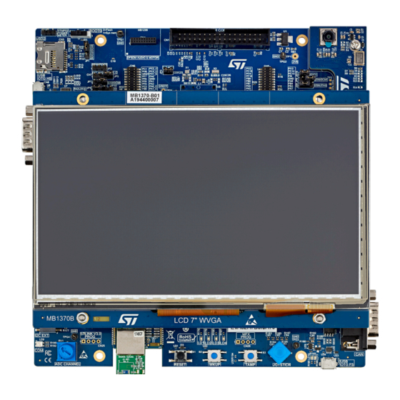
ST STM32H7B3I-EVAL User Manual (95 pages)
With STM32H7B3LI MCU
Brand:
ST
| Category:
Motherboard
| Size: 11 MB
Table of Contents
Figure 1. STM32H7B3I-EVAL Evaluation Board (Top View)
1
1 Features
2
2 Ordering Information
3
Product Marking
3
Codification
3
Table 1. List of Available Products
3
Table 2. Codification Explanation
3
3 Development Environment
4
System Requirements
4
Development Toolchains
4
Demonstration Software
4
4 Conventions
5
Table 3. ON/OFF Convention
5
5 Delivery Recommendations
6
6 Hardware Layout and Configuration
7
Figure 2. Hardware Block Diagram
7
Figure 3. STM32H7B3I-EVAL Evaluation Board Layout
8
Embedded STLINK-V3E
9
Description
9
How to Use
9
Drivers
10
STLINK-V3E Firmware Upgrade
10
Interface
10
Figure 4. USB Composite Device
10
External JTAG, SWD, and Trace
11
Description
11
Figure 5. External Debug Tools Connectors
11
Limitations and Hardware Configuration - ETM Trace (CN15)
12
Table 4. ETM Trace Hardware Configuration
12
Limitations and Hardware Configuration - JTAG (CN14) or MIPI10 (CN16)
13
Interface
13
Table 5. STDC14 / MIPI10 Debugging Connector CN16
13
Table 6. STDC14 / MIPI10 Debug Connector CN16
13
Figure 6. STDC14 / MIPI10 Debugging Connector CN16
13
Table 7. ETM Trace Debugging Connector CN15
14
Figure 7. ETM Trace Debugging Connector CN15
14
Table 8. JTAG / SWD Debugging Connector CN14
15
Figure 8. JTAG Debugging Connector CN14
15
Power Supply
16
Board Power Supply Description
16
Board Power Supply - Hardware Configuration
17
Table 9. Power Related Jumpers
17
Figure 9. Power Supply Connector CN17
18
Board Power Supply - SMPS / LDO Configuration
19
Table 10. Internal SMPS / LDO and Board Configuration
19
Figure 10. MCU Power : SMPS / LDO
19
Figure 11. Config1 - LDO Only
20
Figure 12. Config2 - SMPS Only (Default Configuration)
20
Figure 13. Config3 - SMPS and LDO Cascaded
21
Figure 14. Config4 - External SMPS
21
Board Power Supply - VDD50_USB and VREGOUTV33V
22
Table 11. USB Power Sources
22
Figure 15. MCU Power: USB Regulator
22
Figure 16. VDD50_USB and VREGOUTV33V Schematic
22
Board Power Supply - VDDMMC
23
Table 12. Pins Supplied by VDDMMC but '3.3V Only
23
Figure 17. MCU Power: VDDMMC
23
Table 13. VDDMMC Default Hardware Configuration for '3.3V Only' Functions
24
Table 14. SDIO2 Pins Supplied by VDDMMC (1.8V or 3.3V)
24
Table 15. VDDMMC Hardware Configuration for '1.8V / 3.3V' Function (SDIO2)
25
Figure 18. 3V3_SW_SW_ENABLE and 1V8_SW_ENABLE MFX Schematic
25
Figure 19. 3V3_SW and 1V8_SW Ldos Schematic
26
Figure 20. VDDIO_MMC Switch Schematic
26
Clock, Reset, and Boot
27
Clock Source
27
Table 16. 24 Mhz Crystal X1 Related Solder Bridges
27
Table 17. 32.768 Khz Crystal X2 Related Solder Bridges
27
Figure 21. VDDMMC Schematic
27
Reset Source
28
Boot Option
28
Vcp St-Link Uart
28
Description
28
Operating Voltage
28
Table 18. Boot Related Switch
28
Table 19. Boot Related Jumpers
28
Hardware Configuration
29
Rs-232 Uart
29
Description
29
Operating Voltage
29
Table 20. STLINK-V3E VCP UART (PB14/P15: Default Configuration)
29
Table 21. STLINK-V3E VCP UART (PA2/PA3: Compatible with Bootloader)
29
Table 22. RS-232 UART (PB14/P15: Default Configuration)
29
Interface
30
Table 23. RS-232 UART Related Jumpers (PA2/PA3: Bootloader)
30
Table 24. RS-232 Connector CN9 with ISP Support
30
Figure 22. RS-232 Connector CN9
30
7 Primary Functions
31
Audio
31
Description
31
Operating Voltage
31
Limitations and Hardware Configuration
31
Interface
32
Table 25. Hardware Configuration for CS42L51-CNZ I2S-SAI Communication Bus
32
DFSDM Microphones Module (MB1299)
33
Description
33
Table 26. DFSDM Channel Connection between MCU, MB1331, and MB1299
33
Figure 23. MEMS Beamforming Microphone Module (MB1299)
33
Operating Voltage
34
Limitations and Hardware Configuration
34
Interface
34
Table 27. Hardware Configuration for DFSDM Microphones Module
34
Table 28. MEMS Microphone Module MB1299 and Motor Control Module Connector CN4
34
Figure 24. MEMS Microphone Module and Motor Control Module Connector CN4
34
Usb Otg Fs
35
Description
35
Operating Voltage
35
Limitations and Hardware Configuration
35
Interface
35
Microsd™ Card 1
35
Table 29. USB OTG FS Micro-AB Connector CN27
35
Interface
36
Limitations and Hardware Configuration
36
EXT I 2 C Connector
36
Description
36
Operating Voltage
36
Table 30. Microsd ™ Connector CN28
36
Figure 25. Microsd ™ Connector CN28
36
Interface
37
32-Bit SDRAM
37
Description
37
Operating Voltage
37
Limitations and Hardware Configuration
37
Table 31. EXT I C Connector CN24
37
Figure 26. EXT I C Connector CN24
37
Octo-SPI nor Flash 1
38
Description
38
Operating Voltage
38
Limitations and Hardware Configuration
38
Table 32. Hardware Configuration for SDRAM
38
Analog Input
39
Description
39
Operating Voltage
39
Interface
39
Table 33. OCSPI1 Hardware Configuration
39
Table 34. Analog I/O Connector CN7 Pinout
39
Figure 27. Analog I/O Connector CN7
39
LCD Display Module (MB1370)
40
Description
40
Operating Voltage
40
Limitations and Hardware Configuration
40
Interface
40
Figure 28. Orientation Setting of the 7-Inch LCD Daughterboard
40
Table 35. LCD Module Connector CN23
41
Leds and Buttons
42
Description
42
Table 36. CTP and LCD Power Connector CN30
42
Table 37. LCD RESET Hardware Configuration
42
Table 38. CTP RESET Hardware Configuration
42
Table 39. LCD Module Connector CN23
42
Operating Voltage
43
Camera Module MB1379
43
Description
43
Limitations and Hardware Configuration
43
Table 40. B2 and B3 Buttons
43
Table 41. Hardware Modifications for Camera
44
Interface
45
Wi-Fi
45
Description
45
Operating Voltage
45
Limitations and Hardware Configuration
45
Table 42. Camera Module MB1379 Connector CN2
45
Figure 29. Camera Module Connector CN2
45
Table 43. Hardware Modifications for Wi-Fi
46
Table 44. Wi-Fi ® Module Interposer Connector U24
47
Figure 30. Wi-Fi ® Module Interposer Footprint (Top View)
47
MFX (Multi-Function Expander)
48
Description
48
Operating Voltage
48
Limitations and Hardware Configuration
48
Table 45. MFX Signals
48
Interface
49
8 Secondary Functions
50
Sram
50
Description
50
Operating Voltage
50
Limitations and Hardware Configuration
50
Limitations and Hardware Configuration for SRAM A19 (Just for the Test)
51
Table 46. Configuration for SRAM A0-A5, A10-11 Addresses, and Command
51
Nor
52
Description
52
Operating Voltage
52
Limitations and Hardware Configuration
52
Table 47. Configuration for SRAM A19 (Just for the Test)
52
Limitations and Hardware Configuration for nor A19-A22 (Just for the Test)
53
Table 48. Configuration for nor A0-A5, A10-11 Addresses, and Command
53
Microsd™ Card 2
54
Description
54
Operating Voltage
54
Limitations and Hardware Configuration
54
Table 49. Configuration for SRAM A19-A22 (Just for the Test)
54
Interface
55
Table 50. Configuration for nor A0-A5, A10-11 Addresses, and Command
55
Table 51. Microsd Connector CN3
55
Figure 31. Microsd ™ Connector CN3
55
Usb Otg Hs
56
Description
56
Operating Voltage
56
Limitations and Hardware Configuration
56
Interface
57
DFSDM STMP2 and PT100 Monitoring
57
Description
57
Operating Voltage
57
Limitations and Hardware Configuration
57
Table 52. USB OTG HS Function Configuration
57
Table 53. USB OTG HS Micro-AB Connector CN8
57
OCSPI nor Flash 2 Module (MB1242)
58
Description
58
Operating Voltage
58
Limitations and Hardware Configuration
58
Table 54. OCSPI / HYPERBUS Supported Part Numbers on MB1242
58
Table 55. QSPI / Dual QSPI Supported Part Numbers on MB1242
58
Table 56. OCSPI2 Hardware Configuration
59
Interface
60
Table 57. CN10 (Left) MB1242 Pin-Out
60
Figure 32. MB1242 OCSPI Module Connectors CN10 and CN11
60
Can Fd
61
Description
61
Operating Voltage
61
Limitations and Hardware Configuration
61
Interface
61
Table 58. CN11 (Right) MB1242 Pin-Out
61
Figure 33. CAN D-Type 9-Pin Male Connector CN22
61
Motor Control
62
Description
62
Operating Voltage
62
Limitations and Hardware Configuration
62
Interface
62
Table 59. CN10 (Left) MB1242 Pin-Out
62
Table 60. Motor-Control Legacy Connector CN1 (17X2)
62
Figure 34. Motor-Control Legacy Connector CN1
62
Table 61. Motor-Control DFSDM Connector CN4 (10X2)
63
Figure 35. Motor-Control Legacy Connector CN4
63
FMC Memory Extension Connectors CN12 and CN13
65
Table 62. Memory Connector CN12 Left Odd Pins
65
Table 63. Memory Connector CN12 Left Even Pins
66
Table 64. Memory Connector CN13 Right Odd Pins
67
Table 65. Memory Connector CN13 Right Even Pins
68
Daughterboard Extension Connectors CN5 and CN6
69
Table 66. Daughterboard Extension Connector CN6 Left Odd Pins
69
Table 67. Daughterboard Extension Connector CN6 Left Even Pins
70
Table 68. Daughterboard Extension Connector CN5 Right Odd Pins
71
Table 69. Daughterboard Extension Connector CN5 Right Even Pins
72
Appendix Astm32H7B3I-Eval I/O Assignment
73
Table 70. STM32H7B3I-EVAL I/O Assignment
73
Appendix Bmfx I/O Assignment
78
Table 71. MFX I/O Assignment
78
Appendix Cstm32H7B3I-Eval Mechanical Drawing
79
Table 72. Mechanical Dimensions (in Millimeters)
79
Figure 36. Mechanical Dimensions (in Millimeters)
79
Appendix D Primary Functions Supported by Default
80
Figure 37. Primary Features - Use Case Compatibility Matrix
81
Appendix E Secondary Functions Supported with Limitations
82
Figure 38. Secondary Features - Use Case Compatibility Matrix
82
Appendix F Federal Communications Commission (FCC) and Industry Canada (IC)
83
Compliance Statements
83
FCC Compliance Statement
83
IC Compliance Statement
83
CE Conformity
84
Warning
84
Simplified Declaration of Conformity
84
Revision History
85
Table 73. Document Revision History
85
Advertisement
Advertisement
Related Products
ST STM32H747I-EVAL
ST STM32H757I-EVAL
ST STM32H747I-DISCO
ST STM32H747XI MCU
ST STM32H7 Nucleo-144
ST STM32H735G-DK
ST STM32H753I-EVAL
ST STM32H743I-EVAL
ST STM32H5
ST STM32 Nucleo-64
ST Categories
Motherboard
Computer Hardware
Microcontrollers
Control Unit
Controller
More ST Manuals
Login
Sign In
OR
Sign in with Facebook
Sign in with Google
Upload manual
Upload from disk
Upload from URL