Table of Contents
Advertisement
Advertisement
Table of Contents

Related Manuals for Terasic Altera Cyclone V GX Starter Kit


Summary of Contents for Terasic Altera Cyclone V GX Starter Kit
-
Page 2: Table Of Contents
CONTENTS CHAPTER 1 INTRODUCTION ..........................3 1.1 P ..............................3 ACKAGE ONTENTS 1.2 C V GX S CD ......................4 YCLONE TARTER YSTEM 1.3 L ............................4 AYOUT AND OMPONENTS 1.4 B V GX S ................8 LOCK IAGRAM OF THE YCLONE TARTER OARD... - Page 3 CHAPTER 5 RTL BASED EXAMPLE CODES ...................... 64 5.1 F ............................64 ACTORY ONFIGURATION 5.2 LPDDR2 SDRAM RTL T ..........................65 CHAPTER 6 NIOS-II BASED EXAMPLE CODES ....................68 6.1 SRAM ..................................68 6.2 U LED ..........................71 ART TO CONTROL 6.3 HDMI TX ................................
-
Page 4: Chapter 1 Introduction
Chapter 1 Introduction The Cyclone V GX Starter Kit presents a robust hardware design platform built around the Altera Cyclone V GX FPGA, which is optimized for the lowest cost and power requirement for transceiver applications with industry-leading programmable logic for ultimate design flexibility. With Cyclone V FPGAs, you can get the power, cost, and performance levels you need for high-volume applications including protocol bridging, motor control drives, broadcast video converter and capture cards, and handheld devices. -
Page 5: Kit System Cd
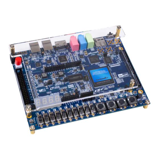
The Cyclone V GX Start Kit System CD contains the documentation and supporting materials, including the User Manual, Control Panel, System Builder, reference designs and device datasheets. User can download this System CD from the web (http://c5g.terasic.com). This chapter presents the features and design characteristics of the board. - Page 6 Figure 1-2 Development Board (top view) Figure 1-3 Development Board (bottom view)
- Page 7 The board has many features that allow users to implement a wide range of designed circuits, from simple circuits to various multimedia projects. The following hardware is provided on the board: • Cyclone V GX 5CGXFC5C6F27C7N Device • 77K Programmable Logic Elements •...
- Page 8 • 24-bit CODEC, Line-in, line-out, and microphone-in jacks • 18 LEDs • 10 Slide Switches • 4 Debounced Push Buttons • 1 CPU reset Push Buttons • 12V DC input...
-
Page 9: Gx Starter Kit Board
FPGA to implement any system design. Figure 1-4 Board Block Diagram Here are the addresses where you can get help if you encounter any problem: • Terasic Technologies Taiwan/ 9F, No.176, Sec.2, Gongdao 5th Rd, East Dist, Hsinchu City, Taiwan 300-70 Email: support@terasic.com... -
Page 10: Chapter 2 Control Panel
Chapter 2 Control Panel The Cyclone V GX Start board comes with a Control Panel program that allows users to access various components on the board from a host computer. The host computer communicates with the board through a USB connection. The program can be used to verify the functionality of components on the board or be used as a debug tool while developing RTL code. - Page 11 Please note that the Control Panel will occupy the USB port until you close that port; you cannot use Quartus II to download a configuration file into the FPGA until the USB port is closed. The Control Panel is now ready for use; experience it by setting the ON/OFF status for some LEDs and observing the result on the C5G board.
- Page 12 The concept of the C5G Control Panel is illustrated in Figure 2-2. The “Control Circuit” that performs the control functions is implemented in the FPGA board. It communicates with the Control Panel window, which is active on the host computer, via the USB Blaster link. The graphical interface is used to send commands to the control circuit.
-
Page 13: Controlling The Led S , 7- Segment Displays
A simple function of the Control Panel is to allow setting the values displayed on LEDs, 7-segment displays. Choosing the tab leads to the window in Figure 2-3. Here, you can directly turn the LEDs on or off individually or by clicking “Light All” or “Unlight All”. Figure 2-3 Controlling LEDs... - Page 14 Choosing the 7-SEG tab leads to the window shown in Figure 2-4. From the window, directly use the left-right arrows to control the 7-SEG patterns on the Cyclone V GX Starter board which are updated immediately. Note that the dots of the 7-SEGs are not enabled on Cyclone V GX Starter Board.
-
Page 15: Switches And Push - Buttons
Choosing the Switches tab leads to the window in Figure 2-5. The function is designed to monitor the status of slide switches and push-buttons in real time and show the status in a graphical user interface. It can be used to verify the functionality of the slide switches and push-buttons. Figure 2-5 Monitoring switches and buttons The ability to check the status of push-button and slide switch is not needed in typical design activities. -
Page 16: Sram/Lpddr2 Controller And Programmer
The Control Panel can be used to write/read data to/from the SRAM and LPDDR2 chips on the Cyclone V GX Starter board. As an example, we will describe how the LPDDR2 may be accessed; the same approach is used to access the SRAM. Click on the Memory tab and select “LPDDR2” to reach the window in Figure 2-6. - Page 17 Specify the number of bytes to be written in the Length box. If the entire file is to be loaded, then a checkmark may be placed in the File Length box instead of giving the number of bytes. To initiate the writing process, click on the Write a File to Memory button. When the Control Panel responds with the standard Windows dialog box asking for the source file, specify the desired file in the usual manner.
-
Page 18: Sd Card
The function is designed to read the identification and specification information of the SD Card. The 4-bit SD MODE is used to access the SD Card. This function can be used to verify the functionality of the SD Card Interface. Follow the steps below to perform the SD Card exercise: Choosing the SD Card tab leads to the window in Figure 2-7. -
Page 19: Uart-Usb Communication
voltage shown is the voltage reading from the separate pins on the extension header. Figure 2-8 shows the ADC readings when the ADC tab is chosen. Figure 2-8 Reading of eight channel ADC The Control Panel allows users to verify the operation of the UART to USB serial communication interface on the Cyclone V GX Starter Board. -
Page 20: Hdmi-Tx
• Baud Rate: 115200 • Parity Check Bit: None • Data Bits: 8 • Stop Bits: 1 • Flow Control (CTS/RTS): OFF To begin the communication, enter specific letters followed by clicking Send. During the communication process, observe the status of the Receive terminal window to verify its operation. -
Page 21: Hsmc
Verify. Please note to turn off the Cyclone V GX Starter board before the HSMC loopback adapter is installed to prevent any damage to the board. The HSMC loopback adapter is not provided in the kit package but can be purchased through the website below: (http://hsmc_loopback.terasic.com) -
Page 22: Overall Structure Of The C5G Control Panel
Figure 2-11 HSMC loopback verification test performed under Control Panel The C5G Control Panel is based on a Nios II Qsys system instantiated in the Cyclone V GX FPGA with software running on the on-chip memory. The software part is implemented in C code; the hardware part is implemented in Verilog HDL code with Qsys builder. - Page 23 Figure 2-12 The block diagram of the C5G control panel...
-
Page 24: Using The Starter Kit
Chapter 3 Using the Starter Kit In this chapter we introduce the important components on the Cyclone V GX Starter Kit. The procedure of downloading a circuit from a host computer to the Cyclone V GX Starter Kit board is described in the tutorial Quartus II Introduction. This tutorial can be found under the \tutorials folder on the Cyclone V GX Starter Kit System CD. - Page 25 disable the JTAG signals on HSMC connector that will form a closed JTAG loop chain on Cyclone V GX Starter Kit board (See Figure 3-2). Thus, only the on-board FPGA device (Cyclone V GX) will be detected by the Quartus II programmer. If users want to include another FPGA device or interface containing FPGA device in the chain via HSMC connector, remove JP2 Jumper (open pin1 and pin2 on JP2) to enable the JTAG signal ports on the HSMC connector.
- Page 26 Configuring the FPGA in JTAG Mode Figure 3-3 illustrates the JTAG configuration setup. To download a configuration bit stream into the Cyclone V GX FPGA, you need to perform the following steps: • Ensure that power is applied to the Cyclone V GX Starter Kit board •...
- Page 27 Configuring the EPCQ256 in AS Mode Figure 3-5 illustrates the AS configuration setup. To download a configuration bit stream into the EPCQ256 serial configuration device, you need to perform the following steps: • Ensure that power is applied to the Cyclone V GX Starter Kit board. •...
-
Page 28: General User Input /Output
3.3-V Power Illuminates when 3.3-V power is active. HSMC_12-V Power Illuminates when HSMC 12-V power is active. HSMC_PSNT_n Illuminates when HSMC Daughter Card is present ULED Illuminates when the on-board USB-Blaster is working Figure 3-6 Status LED position This section describes the user I/O interface to the FPGA. ... - Page 29 depressed. Since the push-button switches are debounced, they are appropriate for using as clocks or reset inputs in a circuit. Table 3-2 lists the board references, signal names, and their corresponding Cyclone V GX device pin numbers. Figure 3-7 Connections between the push-button and Cyclone V GX FPGA Pushbutton depressed Pushbutton released Before...
- Page 30 Table 3-2 Push-button Pin Assignments, Schematic Signal Names, and Functions Board Schematic Cyclone V GX Description Reference Signal Name Standard Pin Number KEY0 KEY0 High Logic Level when the button is not 1.2-V PIN_P11 pressed. The four push buttons (KEY0, KEY1 KEY1 1.2-V...
- Page 31 Table 3-3 Slide Switch Pin Assignments, Schematic Signal Names, and Functions Board Schematic Cyclone V GX Description Reference Signal Name Standard Pin Number Slide Switch[0] 1.2-V PIN_AC9 Slide Switch[1] 1.2-V PIN_AE10 Slide Switch[2] 1.2-V PIN_AD13 Slide Switch[3] 1.2-V PIN_AC8 Slide Switch[4] 1.2-V PIN_W11 Slide Switch[5]...
- Page 32 Table 3-4 User LEDs Pin Assignments, Schematic Signal Names, and Functions Board Schematic Cyclone V GX Description Reference Signal Name Standard Pin Number LEDR0 LEDR0 Driving a logic 1 on the I/O port turns the LED 2.5-V PIN_F7 LEDR1 LEDR1 2.5-V PIN_F6 Driving a logic 0 on the I/O port turns the LED...
- Page 33 Figure 3-11 Connection between 7-segment displays and Cyclone V GX FPGA Figure 3-12 Connections between the 7-segment display HEX0 and Cyclone V GX FPGA Table 3-5 User 7-segment display Pin Assignments, Schematic Signal Names, and Functions Schematic Board Cyclone V GX Signal Description Reference...
-
Page 34: Clock Circuit
HEX0 HEX0_D1 2.5-V PIN_V18 Seven Segment Digit 0[1] HEX0 HEX0_D2 2.5-V PIN_V17 Seven Segment Digit 0[2] HEX0 HEX0_D3 2.5-V PIN_W18 Seven Segment Digit 0[3] HEX0 HEX0_D4 2.5-V PIN_Y20 Seven Segment Digit 0[4] HEX0 HEX0_D5 2.5-V PIN_Y19 Seven Segment Digit 0[5] HEX0 HEX0_D6 2.5-V... - Page 35 Figure 3-13 Clock circuit of the FPGA Board The programming Clock Generator is a highly flexible and configurable clock generator/buffer. The is to provide special and high quality clock signals for high-speed transceivers. The clock generator is controlled by the FPGA through the I2C serial interface. The user can modify the frequency between 0.16 MHz to 200 MHz.
-
Page 36: Rs-232 Serial Port To Usb Interface
Table 3-7 Programmable oscillator control pin, Signal Name, I/O standard, Pin Assignments and Descriptions Programmable Schematic Cyclone V GX I/O Standard Description Oscillator Signal Name Pin Number I2C_SCL 2.5-V PIN_B7 I2C bus, direct U20 (Si5338) connected with Si5338 I2C_SDA 2.5-V PIN_G11 The RS-232 is designed to perform communication between board and PC, allowing a transmission speed of up to 3Mbps. -
Page 37: Sram : Static Random Access Memory
Table 3-9 RS-232 Status LED Board Reference LED Name Description TX LED Illuminates when RS-232 transmit is active. RX LED Illuminates when RS-232 receiving is active. The IS61LV25616AL SRAM (Static Random Access Memory) device is featured on the development board. For detailed information on how to use the SRAM, please refer to the datasheet, which is available on the manufacturer’s website, or under the Datasheets\SRAM folder on the Kit System CD. -
Page 38: Lpddr2 Memory
SRAM_A5 Address bus 3.3-V PIN_C25 SRAM_A6 Address bus 3.3-V PIN_J20 SRAM_A7 Address bus 3.3-V PIN_J21 SRAM_A8 Address bus 3.3-V PIN_D22 SRAM_A9 Address bus 3.3-V PIN_E23 SRAM_A10 Address bus 3.3-V PIN_G20 SRAM_A11 Address bus 3.3-V PIN_F21 SRAM_A12 Address bus 3.3-V PIN_E21 SRAM_A13 Address bus 3.3-V... - Page 39 available on the manufacturer’s website, or under the Datasheets\LPDDR2 folder on the Kit System Figure 3-17 shows the related schematics and Table 3-11 lists the LPDDR2 pin assignments, signal names, and functions. Figure 3-16 Connections between the Cyclone V GX FPGA and LPDDR2 Chip Figure 3-17 LPDDR2 and Cyclone V GX FPGA Table 3-11 LPDDR2 Memory Pin Assignments, Schematic Signal Names, and Functions Schematic...
- Page 40 DDR2LP_CA5 Command/address bus 1.2-V HSUL PIN_U11 DDR2LP_CA6 Command/address bus 1.2-V HSUL PIN_AE9 DDR2LP_CA7 Command/address bus 1.2-V HSUL PIN_AF9 DDR2LP_CA8 Command/address bus 1.2-V HSUL PIN_AB12 DDR2LP_CA9 Command/address bus 1.2-V HSUL PIN_AB11 DDR2LP_DQ0 Data bus 1.2-V HSUL PIN_AA14 DDR2LP_DQ1 Data bus 1.2-V HSUL PIN_Y14 DDR2LP_DQ2 Data bus...
-
Page 41: Micro Sd-Card
DDR2LP_DM0 Data Write Mask (byte enables) 1.2-V HSUL PIN_AF11 DDR2LP_DM1 Data Write Mask (byte enables) 1.2-V HSUL PIN_AE18 DDR2LP_DM2 Data Write Mask (byte enables) 1.2-V HSUL PIN_AE20 DDR2LP_DM3 Data Write Mask (byte enables) 1.2-V HSUL PIN_AE24 DDR2LP_CK_p Differential Output Clock (positive) Differential 1.2-V HSUL PIN_N10 DDR2LP_CK_n... - Page 42 Figure 3-19 Micro SD Card Table 3-12 SD Card Pin Assignments, Schematic Signal Names, and Functions Schematic Cyclone V GX Description I/O Standard Signal Name Pin Number SD_CLK Serial Clock 3.3-V PIN_AB6 SD_CMD Command, Response 3.3-V PIN_W8 SD_DAT0 Serial Data 0 3.3-V PIN_U7 SD_DAT1...
-
Page 43: Hdmi Tx Interface
The development board provides High Performance HDMI Transmitter via the Analog Devices ADV7513 which incorporates HDMI v1.4 features, including 3D video support, and 165 MHz supports all video formats up to 1080p and UXGA. The ADV7513 is controlled via a serial I2C bus interface, which is connected to pins on the Cyclone V GX FPGA. -
Page 44: Audio Interface
HDMI_TX_D14 Video Data bus 3.3-V PIN_N25 HDMI_TX_D15 Video Data bus 3.3-V PIN_P26 HDMI_TX_D16 Video Data bus 3.3-V PIN_P21 HDMI_TX_D17 Video Data bus 3.3-V PIN_R24 HDMI_TX_D18 Video Data bus 3.3-V PIN_R26 HDMI_TX_D19 Video Data bus 3.3-V PIN_AB26 HDMI_TX_D20 Video Data bus 3.3-V PIN_AA24 HDMI_TX_D21... -
Page 45: Hsmc : High -Speed Mezzanine Card
Figure 3-21 Connections between FPGA and Audio CODEC Table 3-14 Audio CODEC Pin Assignments, Schematic Signal Names, and Functions Schematic Cyclone V GX Description I/O Standard Signal Name Pin Number AUD_ADCLRCK Audio CODEC ADC LR Clock 2.5-V PIN_C7 AUD_ADCDAT Audio CODEC ADC Data 2.5-V PIN_D7 AUD_DACLRCK... - Page 46 maximum power consumption for the HSMC connector. Note that the +12V DC power rail goes through a jumper (See Figure 3-22). The function of the jumper is to avoid cases when users no longer use the 12V power, and the power goes directly to HSMC daughter boards and thus leads to burning the FPGA I/Os.
- Page 47 There are three banks in this connector. Figure 3-23 shows the bank arrangement of signals with respect to the SAMTEC connector. Table 3-16 lists the mapping of the FPGA pin assignments to the HSMC connectors. Figure 3-23 HSMC Signal Bank Diagram Table 3-16 Power Supply of the HSMC Supplied Voltage Max.
-
Page 48: Input/Output
differential clock input HSMC_CLKIN_p1 LVDS RX or CMOS I/O or 2.5-V or LVDS PIN_G15 differential clock input HSMC_CLKIN_p2 LVDS RX or CMOS I/O or 2.5-V or LVDS PIN_L8 differential clock input HSMC_CLKOUT0 Dedicated clock output 2.5-V PIN_A7 HSMC_CLKOUT_n1 LVDS TX or CMOS I/O or 2.5-V or LVDS PIN_A18 differential clock input/output... - Page 49 HSMC_RX _n9 LVDS RX bit 9n or CMOS I/O LVDS or 2.5-V PIN_E15 HSMC_RX _n10 LVDS RX bit 10n or CMOS I/O LVDS or 2.5-V PIN_D13 HSMC_RX _n11 LVDS RX bit 11n or CMOS I/O LVDS or 2.5-V PIN_D15 HSMC_RX _n12 LVDS RX bit 12n or CMOS I/O LVDS or 2.5-V PIN_D16...
-
Page 50: Using The
HSMC_TX _p3 LVDS TX bit 3 or CMOS I/O LVDS or 2.5-V PIN_A12 HSMC_TX _p4 LVDS TX bit 4 or CMOS I/O LVDS or 2.5-V PIN_B10 HSMC_TX _p5 LVDS TX bit 5 or CMOS I/O LVDS or 2.5-V PIN_C20 HSMC_TX _p6 LVDS TX bit 6 or CMOS I/O LVDS or 2.5-V PIN_B15... - Page 51 The 40-pin header connects directly to 36 pins of the Cyclone V GX FPGA, and also provides DC +5V (VCC5), DC +3.3V (VCC3P3), and two GND pins. Figure 3-25 shows the I/O distribution of the GPIO connector. The maximum power consumption of the daughter card that connects to GPIO port is shown in Table 3-18.
- Page 52 Each pin on the expansion headers is connected to two diodes and a resistor that provides protection against high and low voltages. Figure 3-26 shows the protection circuitry for only one of the pin on the header, but this circuitry is applied for all 36 data pins. Figure 3-26 Connections between the GPIO connector and Cyclone V GX FPGA Table 3-19 Pin Assignments for 40-pin Expansion Header connector and share bus signal.
- Page 53 GPIO11 Arduino_IO8 GPIO DATA[11] , Arduino IO8 3.3-V PIN_U22 GPIO12 Arduino_IO9 GPIO DATA[12] , Arduino IO9 3.3-V PIN_P8 GPIO13 Arduino_IO10 GPIO DATA[13] , Arduino IO10 3.3-V PIN_R8 GPIO14 Arduino_IO11 GPIO DATA[14] , Arduino IO11 3.3-V PIN_R9 GPIO15 Arduino_IO12 GPIO DATA[15] , Arduino IO12 3.3-V PIN_R10 GPIO DATA[16] , Arduino IO13,...
- Page 54 Figure 3-27 Arduino Pin Arrangement and Connections. Table 3-20 lists the all the pin assignments of the Arduino Uno connector (digital), signal names relative to the Cyclone V GX device. Table 3-20 Pin Assignments for Arduino Uno Expansion Header connector Schematic Cyclone V GX Description...
- Page 55 Besides 14 pins for digitial GPIO, there are also 8 analog inputs on the Arduino Uno Expansion Header. Consequently, we use ADC LTC2308 from Linear Technology on the board for possible future analog-to-digital applications. The LTC2308 is a low noise, 500ksps, 8-channel, 12-bit ADC with an SPI/MICROWIRE compatible serial interface.
- Page 56 Table 3-21 ADC SPI Interface Pin Assignments, Schematic Signal Names, and Functions Schematic Cyclone V GX Description I/O Standard Signal Name Pin Number ADC_CONVST Conversion Start 1.2-V PIN_AB22 ADC_SCK Serial Data Clock 1.2-V PIN_AA21 ADC_SDI Serial Data Input (FPGA to ADC) 1.2-V PIN_Y10 ADC_SDO...
-
Page 57: Chapter 4 System Builder
Chapter 4 System Builder This chapter describes how users can create a custom design project on the board by using the Software Tool of Cyclone V GX Starter Kit – C5G System Builder. The C5G System Builder is a Windows-based software utility, designed to assist users to create a Quartus II project for the board within minutes. -
Page 58: Using C5G System Builder
design/logic. The Quartus II setting file contains information such as FPGA device type, top-level pin assignment, and the I/O standard for each user-defined I/O pin. Finally, the Quartus II programmer must be used to download SOF file to the development board using a JTAG interface. - Page 59 Figure 4-2 The SoCKit System Builder window Input Project Name Input project name as show in Figure 4-3. Project Name: Type in an appropriate name here, it will automatically be assigned as the name of your top-level design entity. Figure 4-3 Board Type and Project Name...
- Page 60 System Configuration Under the System Configuration users are given the flexibility of enabling their choice of included components on the board as shown in Figure 4-4. Each component of the board is listed where users can enable or disable a component according to their design by simply marking a check or removing the check in the field provided.
- Page 61 Figure 4-5 GPIO Expansion The “Prefix Name” is an optional feature that denotes the pin name of the daughter card assigned in your design. Users may leave this field empty. Arduino Expansion Users can connect Arduino daughter cards onto the Arduino connector located on the development board.
- Page 62 Figure 4-6 Arduino Expansion HSMC Expansion Users can connect HSMC daughter cards onto the HSMC connector located on the development board. As shown in Figure 4-7, select the daughter card you wish to add to your design under the appropriate HSMC connector to which the daughter card is connected.
- Page 63 Figure 4-7 HSMC Expansion The “Prefix Name” is an optional feature that denotes the pin name of the daughter card assigned in your design. Users may leave this field empty. Project Setting Management The C5G System Builder also provides functions to restore default setting, loading a setting, and saving users’...
- Page 64 Figure 4-8 Project Settings Project Generation When users press the Generate button, the C5G System Builder will generate the corresponding Quartus II files and documents as listed in the Table 4-1: Table 4-1 The files generated by C5G System Builder Filename Description <Project name>.v...
-
Page 65: Rtl Based Example Codes
Chapter 5 RTL Based Example Codes This chapter provides a number of RTL based example codes designed for the starter board. All of the associated files can be found in the Demonstrations folder on the System CD. The C5G board is shipped from the factory with a default configuration bit-stream that demonstrates some of the basic features of the board. -
Page 66: Lpddr2 Sdram Rtl Test
Restore Factory Configuration • Ensure that power is applied to the C5G board. • Connect the supplied USB cable to the USB Blaster port on the C5G board. • Configure the JTAG programming circuit by setting the RUN/PROG slide switch (SW11) to the PROG position. - Page 67 Altera LPDDR2 SDRAM Controller with UniPHY To use the Altera LPDDR2 controller, users need to perform three major steps: 1. Create correct pin assignments for the LPDDR2. 2. Setup correct parameters in LPDDR2 controller dialog. 3. Perform “Analysis and Synthesis” by selecting from the Quartus II menu: ProcessStartStart Analysis &...
- Page 68 • Press KEY0 again to regenerate the test control signals for a repeat test. Table 5-1 LED Indicators Table 5-2NAME Description LEDG0 Reset LEDG1 If light, LPDDR2 test pass LEDG2 Blinks...
-
Page 69: Nios-Ii Based Example Codes
Chapter 6 NIOS-II Based Example Codes This chapter provides a number of NIOS-II bases example codes designed for the starter board. These examples provide demonstrations of the major features which connected to FPGA interface on the board, such as audio, video, uart to usb, sdcard, sram, lpddr2 adn HDMI. All of the associated files can be found in the Demonstrations folder on the System CD. - Page 70 Figure 6-1 Block diagram of the SRAM Basic Demonstration The system flow is controlled by a Nios II program. First, the Nios II program writes test patterns into the whole 512KB of SRAM. Then, it calls Nios II system function, alt_dache_flush_all, to make sure all data has been written to SRAM.
- Page 71 Demonstration Batch File Demo Batch File Folder: C5G_SRAM demo_batch The demo batch file includes following files: • Batch File for USB-Blaster : C5G_SRAM.bat, C5G_SRAM.sh • FPGA Configure File : C5G_SRAM.sof • Nios II Program: C5G_SRAM.elf Demonstration Setup • Make sure Quartus II and Nios II are installed on your PC. •...
-
Page 72: Uart To Usb Control Led
Figure 6-2 Many applications need communication with computer through common port ,the traditional connector is RS232 which need to connect to RS232 cable. But today many personal computers don't have the RS232 connector which makes it very inconvenient to develop some projects. The C5G board was designed to support UART communication through USB cable. - Page 73 Figure 6-3 Block diagram of UART Control LED demonstration Design Tools • Quartus II 13.0 • Nios II Eclipse 13.0 Demonstration Source Code • Quartus Project directory: C5G_UART • Nios II Eclipse: C5G_UART\Software Nios II Project Compilation Before you attempt to compile the reference design under Nios II Eclipse, make sure the project is cleaned first by clicking ‘Clean’...
- Page 74 The demo batch file includes following files: • Batch File for USB-Blaster: C5G_UART_USB_LED.bat, C5G_UART_USB_LED.sh • FPGA Configure File : C5G_UART_USB_LED.sof • Nios II Program: C5G_UART_USB_LED.elf Demonstration Setup • Connect a USB cable between your computer and the C5G board. •...
- Page 75 Figure 6-5 Check the assigned Com Port number On PC • Open the putty software and setup the parameter as shown in Figure 6-5 and click open button to open the terminal. Figure 6-6 putty terminal setup • Make sure Quartus II and Nios II are installed on your PC.
-
Page 76: Hdmi Tx
• Connect USB Blaster to the C5G board and install USB Blaster driver if necessary. • Execute the demo batch file “ C5G_UART_USB_LED.bat” under the batch file folder C5G_USRT \demo_batch. • the nios II-terminal and putty terminal running result as shown in Figure 6-6. - Page 77 Pixel Data [23:0] R[7:0] G[7:0] B[7:0] Figure 6-8 Build-in Display Modes of the HDMI TX Demonstration A set of display modes are implemented for presenting the generated video patterns. The module “Video Source Selector” controls the selection of current video timing among build-in display modes listed in Table 6-1.
- Page 78 Figure 6-9 Block Diagram of the HDMI TX Demonstration A NIOS-II softcore is used to execute user program and send control-commands to the HDMI encoder via the I2C interface. The interrupt events from the HDMI encoder are sent back to the NIOS-II softcore via the HDMI_TX_INT signal.
- Page 79 Design Tools • Quartus II 13.0sp1 • Nios II Eclipse 13.0sp1 Demonstration Source Code • Quartus Project directory: C5G_HDMI_VPG • Nios II Eclipse: C5G_HDMI_VPG\Software Rebuild the Quartus II Project Launch the " Quartus II 13.0sp1" program. Open the project file through the drop-down menu "File"...
- Page 80 • Right-click on the HDMI_DEMO_bsp project in the Project Explore. Select "Nios II" -> "Generate BSP." • Right-click on the HDMI_DEMO_bsp project in the Project Explore. Select "Clean Project." • Right-click on the HDMI_DEMO_bsp project in the Project Explore. Select "Build Project." •...
- Page 81 Figure 6-10 Launching the HDMI TX Demonstration using the "demo_batch" Folder • Wait for a few seconds for the LCD monitor to power up itself. And you should see a pre-defined video pattern shown on the monitor, as shown in Figure 6-10.
- Page 82 When the HDMI encoder is powered up, a sample video pattern will be displayed on the LCD monitor. If the cable is un-plugged, the HDMI encoder will power off automatically to save the power consumption. If the LCD monitor didn't power up automatically when performing activities described above in this demonstration, users can try to completely switch off the power of the LCD monitor and then switch on again.
- Page 83 monitor. Dump the first 256 bytes EDID raw data of the currently connected LCD monitor. In addition, print the decoded result in a human-readable format. Perform a full-dump of the HDMI encoder register set. Power off the HDMI encoder. Power on the HDMI encoder and initialize it in HDMI mode. Power on the HDMI encoder and initialize it in DVI mode.
-
Page 84: Transceiver Hsmc Loopback Test
The XCVR HSMC loopback demonstration is a project to test XCVR HSMC Loopback function. The system generate data pattern and transport data through the xcvr channel. Meanwhile, the system receives the data through the loopback daughter card and checks it. Altera IP data pattern generator and data pattern checker are responsible for generating and checking the data pattern. -
Page 85: Audio Recording And Playing
• Execute the demo batch file “ C5G_HSMC_XCVR_LOOPBACK_TEST.bat” for USB-Blaster II under the batch file folder, C5G_HSMC_XCVR_LOOPBACK_TEST \demo_batch. • After Nios II program is downloaded and executed successfully, a prompt message will be displayed in nios2-terminal and the program will test XCVR HSMC loopback function. •... - Page 86 Figure 6-14 Man-Machine Interface of Audio Recorder and Player Figure 6-15 shows the block diagram of the Audio Recorder and Player design. There are hardware and software parts in the block diagram. The software part stores the Nios II program in the on-chip memory.
- Page 87 Figure 6-15 Block diagram of the audio recorder and player Demonstration File Locations • Hardware Project directory: C5G_Audio • Bit stream used: C5G_Audio.sof • Software Project directory: C5G_Audio\software Demonstration Setup and Instructions • Connect an Audio Source to the LINE-IN port of the C5G board. •...
-
Page 88: Micro Sd Card File System Read
Table 6-4 Slide switch setting for sample rate switching for audio recorder and player (0 – DOWN; (0 – DOWN; (0 – DOWN; Sample Rate 1- UP) 1-UP) 1-UP) 44.1K Unlisted combination Note: C5G_Audio C5G_Audio (1). Execute \demo_batch\ .bat will download .sof and .elf files. (2). - Page 89 Figure 6-16 Block diagram of the Micro SD demonstration Figure 6-17 shows the software stack of this demonstration. The Nios PIO block provides basic IO functions to access hardware directly. The functions are provided from Nios II system and the function prototype is defined in the header file <io.h>.
- Page 90 Figure 6-17 Software of micro SD demonstration Design Tools • Quartus II 13.0 • Nios II Eclipse 13.0 Demonstration Source Code • Quartus Project directory: C5G_SD_DEMO • Nios II Eclipse: C5G_SD_DEMO\Software Nios II Project Compilation • Before you attempt to compile the reference design under Nios II Eclipse, make sure the project is cleaned first by clicking ‘Clean’...
- Page 91 C5G_SD_DEMO.sh • FPGA Configure File : C5G_SD_DEMO.sof • Nios II Program:C5G_SD_DEMO.elf Demonstration Setup • Make sure Quartus II and Nios II are installed on your PC. • Power on the C5G board. • Connect USB Blaster to the C5G board and install USB Blaster driver if necessary. •...
-
Page 92: Sd Card Music Player Demonstration
• Press KEY3 of the C5G board to start reading SD Card. • The program will display SD Card information, as shown in Figure 6-19 Figure 6-19 Running result of SD_CARD demo on C5G board Many commercial media/audio players use a large external storage device, such as an SD Card or CF card, to store music or video files. - Page 93 connected to the keys, leds and switches. Figure 6-20 Block diagram of Micro SD music player Figure 6-21 shows the software stack of this demonstration. SD 4-Bit Mode block implements the SD 4-Bit mode protocol for reading raw data from the SD Card. The FAT block implements FAT16/FAT32 file system for reading wave files that is stored in the SD Card.
- Page 94 Figure 6-21 Software Stack of the Micro SD music player The audio chip should be configured before sending audio signal to the audio chip. The main program uses I2C protocol to configure the audio chip working in master mode; the audio output interface working in I2S 16-bits per channel and with sampling rate according to the wave file contents.
- Page 95 Demonstration Source Code • Quartus Project directory: C5G_SD_MUSIC • Nios II Eclipse: C5G_SD_MUSIC\Software Nios II Project Compilation Before you attempt to compile the reference design under Nios II Eclipse, make sure the project is cleaned first by clicking ‘Clean’ from the ‘Project’ menu of Nios II Eclipse. ...
Need help?
Do you have a question about the Altera Cyclone V GX Starter Kit and is the answer not in the manual?
Questions and answers