Table of Contents
Advertisement
Advertisement
Table of Contents

Related Manuals for Terasic De0-Nano


Summary of Contents for Terasic De0-Nano
-
Page 2: Table Of Contents
4.3 Switches and Pushbuttons ........................28 4.4 Memory Controller ..........................29 4.5 Digital Accelerometer ..........................31 4.6 ADC ............................... 32 4.7 Overall Structure of the DE0-Nano Control Panel .................. 33 CHAPTER 5 DE0-NANO SYSTEM BUILDER..................34 5.1 Introduction ............................34... - Page 3 5.2 General Design Flow ..........................34 5.3 Using DE0-Nano System Builder ......................36 CHAPTER 6 TUTORIAL: CREATING AN FPGA PROJECT ............. 40 6.1 Design Flow ............................40 6.2 Before You Begin ........................... 41 6.3 What You Will Learn ..........................45 6.4 Assign The Device ..........................
- Page 4 9.3 Revision History ........................... 155 9.4 Copyright Statement ..........................155...
-
Page 5: Features
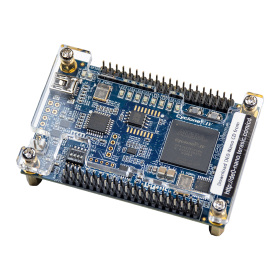
National Semiconductor 8-channel 12-bit A/D converter, and it also features an Analog Devices 13-bit, 3-axis accelerometer device. The DE0-Nano board includes a built-in USB Blaster for FPGA programming, and the board can be powered either from this USB port or by an external power source. The board includes expansion headers that can be used to attach various Terasic daughter cards or other devices, such as motors and actuators. - Page 6 The key features of the board are listed below: Featured device o Altera Cyclone® IV EP4CE22F17C6N FPGA o 153 maximum FPGA I/O pins Configuration status and set-up elements o On-board USB-Blaster circuit for programming o Spansion EPCS64 Expansion header o Two 40-pin Headers (GPIOs) provide 72 I/O pins, 5V power pins, two 3.3V power pins and four ground pins ...
- Page 7 The kit comes with the following contents: DE0-Nano board System CD-ROM. USB Cable The system CD contains technical documents for the DE0-Nano board, which includes component datasheets, demonstrations, schematic, and user manual. Figure 1-2 shows the photograph of the DE0-Nano kit contents.
- Page 8 Chapter 2 DE0-Nano Board Architecture This chapter describes the architecture of the DE0-Nano board including block diagram and components. The picture of the DE0-Nano board is shown in Figure 2-1 Figure 2-2. It depicts the layout of the board and indicates the locations of the connectors and key components.
-
Page 9: Block Diagram Of The De0-Nano Board
Figure 2-2 The DE0-Nano Board PCB and component diagram (bottom view) Figure 2-3 shows the block diagram of the DE0-Nano board. To provide maximum flexibility for the user, all connections are made through the Cyclone IV FPGA device. Thus, the user can configure the FPGA to implement any system design. -
Page 10: Power-Up The De0-Nano Board
1. Connect a USB Mini-B cable between a USB (Type A) host port and the board. For communication between the host and the DE0-Nano board, it is necessary to install the Altera USB Blaster driver software. - Page 11 DE0-Nano board is turned off. When the board’s power is turned on, the configuration data in the EPCS64 device is automatically loaded into the Cyclone IV E FPGA.
- Page 12 Figure 3-1 Programming a serial configuration device with serial flash loader solution JTAG Chain on DE0-Nano Board The JTAG Chain on the DE0-Nano board is connected to a host computer using an on-board USB-blaster. The USB-blaster consists of a USB Mini-B connector, a FTDI USB 2.0 Controller, and an Altera MAX II CPLD.
- Page 13 Schmitt Trigger Debounced Figure 3-4 Pushbuttons debouncing LEDs There are 8 green user-controllable LEDs on the DE0-Nano board. The eight LEDs, which are presented in Figure 3-4, allow users to display status and debugging information. Each LED is driven directly by the Cyclone IV E FPGA. Each LED is driven directly by a pin on the Cyclone IV E FPGA;...
- Page 14 Figure 3-5 Connections between the LEDs and Cyclone IV FPGA DIP Switch The DE0-Nano board contains a 4 dip switches. A DIP switch provides, to the FPGA, a high logic level when it is in the DOWN position, and a low logic level when in the UPPER position.
- Page 15 Table 3-3 Pin Assignments for DIP Switches Signal Name FPGA Pin No. Description I/O Standard DIP Switch[0] PIN_M1 DIP Switch[0] 3.3V DIP Switch[1] PIN_T8 DIP Switch[1] 3.3V DIP Switch[2] PIN_B9 DIP Switch[2] 3.3V DIP Switch[3] PIN_M15 DIP Switch[3] 3.3V The board features a Synchronous Dynamic Random Access Memory (SDRAM) device providing 32MB with a 16-bit data lines connected to the FPGA.
- Page 16 SDRAM Chip Select 3.3V The DE0-Nano contains a 2Kbit Electrically Erasable PROM (EEPROM). The EEPROM is configured through a 2-wire I2C serial interface. The device is organized as one block of 256 x 8-bit memory. The I2C write and read address are 0xA0 and 0xA1, respectively.
- Page 17 PIN_F1 EEPROM data 3.3V The DE0-Nano board provides two 40-pin expansion headers. Each header connects directly to 36 pins of the Cyclone IV E FPGA, and also provides DC +5V (VCC5), DC +3.3V (VCC33), and two GND pins. Figure 3-8...
- Page 18 Figure 3-8 Pin arrangement of the GPIO expansion headers The pictures below indicate the pin 1 location of the expansion headers. Figure 3-9 Pin1 locations of the GPIO expansion headers Table 3-6 GPIO-0 Pin Assignments Signal Name FPGA Pin No. Description I/O Standard 3.3V...
- Page 19 GPIO_02 PIN_A2 3.3V GPIO Connection DATA GPIO_03 PIN_A3 3.3V GPIO Connection DATA GPIO_04 PIN_B3 3.3V GPIO Connection DATA 3.3V GPIO_05 PIN_B4 GPIO Connection DATA 3.3V GPIO_06 PIN_A4 GPIO Connection DATA GPIO_07 PIN_B5 3.3V GPIO Connection DATA GPIO_08 PIN_A5 3.3V GPIO Connection DATA 3.3V GPIO_09 PIN_D5...
- Page 20 3.3V GPIO Connection DATA The DE0-Nano contains an ADC128S022 lower power, eight-channel CMOS 12-bit analog-to-digital converter. This A-to-D provides conversion throughput rates of 50 ksps to 200 ksps. It can be configured to accept up to eight input signals at inputs IN0 through IN7. This eight input signals are connected to the 2x13 header, as shown in Figure 3-10.
- Page 21 Figure 3-10 Pin distribution of the 2x13 Header Figure 3-11 shows the connections on the 2x13 header, A/D converter and Cyclone IV device. Figure 3-11 Wiring for 2x13 header and A/D converter The pictures below indicate the pin 1 location of the 2x13 header.
- Page 22 Figure 3-12 Pin1 locations of the 2x13 header Table 3-8 Pin Assignments for 2x13 Header Signal Name FPGA Pin No. Description I/O Standard GPIO_2[0] PIN_A14 GPIO Connection DATA[0] 3.3V GPIO_2[1] PIN_B16 GPIO Connection DATA[1] 3.3V GPIO_2[2] PIN_C14 GPIO Connection DATA[2] 3.3V GPIO_2[3] PIN_C16...
- Page 23 The DE0-Nano board includes a 50 MHz oscillator. The oscillator is connected directly to a dedicated clock input pin of the Cyclone IV E FPGA. The 50MHz clock input can be used as a source clock to drive the phase lock loops (PLL) circuit. The clock distribution on the DE0-Nano board is shown in Figure 3-14.
- Page 24 Figure 3-14 Block diagram of the clock distribution The DE0-Nano board’s power is provided through the USB 5V power, the 5V VCC pins on the two 40-pin headers or the 2-pin power header. The DC voltage is then stepped down to various required voltages.
- Page 25 Power Distribution System Figure 3-16 shows the power distribution system on the DE0-Nano board. Figure 3-16 DE0-Nano Power Distribution System...
- Page 26 “DE0_NANO_ControlPanel.exe”. When Control Panel starts it will attempt to download a configuration file onto the DE0-Nano board. The configuration file contains a design that communicates with the peripheral devices on the board that are attached to the FPGA device.
- Page 27 LEDs and observing the result on the DE0-Nano board. Figure 4-1 The DE0-Nano Control Panel 4-2. The “Control Circuit” that The concept of the DE0-Nano Control Panel is illustrated in Figure performs the control functions is implemented in the FPGA board. It communicates with the Control Panel window, which is active on the host computer, via the USB Blaster link.
-
Page 28: Sdram Memory
The DE0-Nano Control Panel can be used to light up LEDs, change the buttons/switches status, read/write to SDRAM Memory, read ADC channels, and display the Accelerometer information. A simple function of the Control Panel is to allow setting the values displayed on LEDs. Choosing... - Page 29 The Control Panel can be used to write/read data to/from the SDRAM/EEPROM/EPCS on the DE0-Nano board. As an example, we will describe how the SDRAM may be accessed; the same approach is used to access the EEPROM and EPCS. Click on the Memory tab and select “SDRAM”...
- Page 30 Figure 4-5 Accessing the SDRAM A 16-bit word can be written into the SDRAM by entering the address of the desired location, specifying the data to be written, and pressing the Write button. Contents of the location can be read by pressing the Read button.
-
Page 31: Digital Accelerometer
Figure 4-6 shows the current digital accelerometer status of the DE0-Nano when Accelerometer tab is clicked. The units that are displayed are the raw register values converted to decimal. The value in parentheses is the gravitational acceleration values (mg) calculated from the register values according the formula. - Page 32 Figure 4-6 Digital Accelerometer status From the Control Panel, users are able to view the eight-channel 12-bit analog-to-digital converter reading. The values shown are the ADC register outputs from all of the eight separate channels. The voltage shown is the voltage reading from the separate pins on the extension header. Figure 4-7 shows the ADC readings when the ADC tab is chosen.
- Page 33 The DE0-Nano Control Panel is based on a Nios II SOPC system instantiated in the Cyclone IV E FPGA with software running on the on-chip memory. The software part is implemented in C code; the hardware part is implemented in Verilog HDL code with SOPC builder. The source code is not available on the DE0-Nano System CD.
- Page 34 System Builder software. The software will then prompt you to specify the name of the project you wish to create, as well as the components on the DE0-Nano board you wish to you. Once your specification is complete, you can generate the system.
- Page 35 Quartus II, and then use the Quartus II Programmer tool to configure the FPGA on the DE0-Nano board, using the JTAG programming mode. Figure 5-1 The general design flow of building a design...
- Page 36 Install and launch the DE0-Nano System Builder The DE0-Nano System Builder is located in the directory: "Tools\DE0_NANO_SystemBuilder" on the DE0-Nano System CD. Users can copy the whole folder to a host computer without installing the utility. Launch the DE0-Nano System Builder by executing the DE0_NANO_SystemBuilder.exe...
-
Page 37: System Configuration
If the component is enabled, the DE0-Nano System Builder will automatically generate the associated pin assignments including the pin name, pin location, pin direction, and I/O standard. - Page 38 Users can connect GPIO expansion card onto GPIO header located on the DE0-Nano board as shown in Figure 5-5. Select the appropriate daughter card you wish to include in your design from the drop-down menu. The system builder will automatically generate the associated pin assignments including the pin name, pin location, pin direction, and IO standard.
- Page 39 Figure 5-6 Project Settings Project Generation When users press the Generate button, the DE0-Nano System Builder will generate the corresponding Quartus II files and documents as listed in the Table 5-1: Table 5-1 The files generated by DE0-Nano System Builder...
- Page 40 This tutorial provides comprehensive information for understanding how to create a FPGA design and run it on the DE0-Nano development and education board. The following sections provide a quick overview of the design flow, explaining what is needed to get started, and describe what is taught in this tutorial.
- Page 41 Determined that the development board functions properly and is connected to your computer. Next step is to install the USB-Blaster driver, if not already done. To install the driver, connect a USB cable between the DE0-Nano board and a USB port on a computer that is running the Quartus II software.
- Page 42 Figure 6-2 Found New Hardware Wizard The desired driver is not available on the Windows Update Web site, therefore select “No, not this time” and click Next. This leads to the window in Figure 6-3. Figure 6-3 The driver is found in a specific location...
- Page 43 The driver is available within the Quartus II software. Hence, select “Install from a list or specific location” and click Next to get to Figure 6-4. Figure 6-4 Specify the location of the driver Now, select “Search for the best driver in these locations” and click Browse to get to the pop-up dialog box in Figure 6-5 Find the desired driver, which is at location...
- Page 44 Figure 6-5 Browse to find the location Figure 6-6 There is no need to test the driver...
- Page 45 Of course, you can use your DE0-Nano board to run other designs as well. For the LED design, you will write Verilog HDL code for a simple 32-bit counter, add a phase-locked loop (PLL) megafunction as the clock source, and add a 2-input multiplexer megafunction.
- Page 46 1. In the Quartus II software, select File > New Project Wizard. The Introduction page opens, as shown in Figure 6-8. Figure 6-8 New Project Wizard introduction 2. Click Next. 3. Enter the following information about your project: (Note: File names, project names, and directories in the Quartus II software cannot contain spaces.) a.
- Page 47 Figure 6-9 Project information d. Click Next. e. In the next dialog box, you will assign a specific FPGA device to the design. Select the EP4CE22F17C6 device, as it is the FPGA on the DE0-Nano, as shown in Figure 6-10.
- Page 48 Figure 6-10 Specify the Device Example Click Finish. 4. When prompted, select Yes to create the my_first_fpga project directory. You just created your Quartus II FPGA project. Your project is now open in Quartus II, as shown in Figure 6-11.
- Page 49 Figure 6-11 my_first_fpga project This section describes how to create an FPGA design. This includes creating the top-level design, adding components (in Verilog HDL and using the megafunctions), adding pins and interconnecting all the components and pins. First, create a top-level module. In this tutorial, you will use schematic entry, via a Block Design File (.bdf).
- Page 50 Figure 6-12 New BDF 2. Click OK. 3. Select File > Save As and enter the following information. File name: my_first_fpga Save as type: Block Diagram/Schematic File (*.bdf) 4. Click Save. The new design file appears in the Block Editor (see Figure 6-13).
- Page 51 Figure 6-13 Bank BDF Adding a Verilog HDL to the Schematic 1. Add HDL code to the blank block diagram by choosing File > New > Verilog HDL File. 2. Select Verilog HDL File in the tree and Click OK. 3.
- Page 52 Figure 6-14 Saving the Verilog HDL file The resulting empty file is ready for you to enter the Verilog HDL code. 4. Type the following Verilog HDL code into the blank simple_counter.v file, as shown in Figure 6-15. //It has a single clock input and a 32-bit output port module simple_counter ( CLOCK_5, counter_out...
- Page 53 always @ (posedge CLOCK_5) // on positive clock edge begin counter_out <= counter_out + 1;// increment counter endmodule // end of module counter Figure 6-15 The Verilog File of simple_counter.v 5. Save the file by choosing File > Save, pressing Ctrl + S, or by clicking the floppy disk icon. 6.
- Page 54 9. Right click in the blank area of the BDF file, and select Insert > Symbol. 10. Double-click the Project directory to expand it. 11. Select the newly created simple_counter symbol by clicking its icon. Figure 6-17 Adding the Symbol to the BDF 12.
- Page 55 This tutorial design uses a PLL clock source to drive a simple counter. A PLL uses the on-board oscillator (DE0-Nano Board is 50 MHz) to create a constant clock frequency as the input to the counter. To create the clock source, you will add a pre-built LPM megafunction named ALTPLL.
- Page 56 Figure 6-20): a. Select I/O > ALTPLL. b. Under “Which device family will you be using?” select the Cyclone IV E for DE0-Nano development board. c. Under “Which type of output file do you want to create?” select Verilog HDL.
- Page 57 d. Click Next. Figure 6-21 MegaWizard Plug-In Manager [page 3 of 14] Selections 6. Unselect all options on MegaWizard page 4. As you turn them off, pins disappear from the PLL block’s graphical preview. See Figure 6-22 for an example.
- Page 58 Figure 6-22 MegaWizard Plug-In Manager [page 4 of 14] Selections 7. Click Next four times to get to page 8. 8. Set the Clock division factor to 10, as shown in Figure 6-23.
- Page 59 Figure 6-23 MegaWizard Plug-In Manager [page 8 of 14] Selections Click Next and then click Finish. 10. The wizard displays a summary of the files it creates (see Figure 6-24). Select the pll.bsf option and click Finish again.
- Page 60 Figure 6-24 Wizard-Created Files The Symbol window opens, showing the newly created PLL megafunction,a s shown in Figure 6-25.
- Page 61 Figure 6-25 PLL Symbol 11. Click OK and place the pll symbol onto the BDF to the left of the simple_counter symbol. You can drag and drop the symbols, if you need to rearrange them. See Figure 6-26. Figure 6-26 Place the PLL Symbol 12.
- Page 62 Figure 6-27 Draw a Bus Line connect pll c0 port to simple_counter CLOCK_5 port Adding an Input pin to the Schematic The following steps describe how to add an input pin to the schematic. 1. Right click in the blank area of the BDF and select Insert > Symbol. 2.
- Page 63 4. Place the new pin onto the BDF so that it is touching the input to the pll symbol. 5. Use the mouse to click and drag the new input pin to the left; notice that the ports remain connected as shown in Figure 6-29.
- Page 64 Figure 6-30 Change the input port name 2. Right-click the new output bus line and select Properties. 3. Type counter [31..0] as the bus name (see Figure 6-31). The notation [X ..Y] is the Quartus II method for specifying the bus width in BDF schematics, where X is the most significant bit (MSB) and Y is the least significant bit (LSB).
- Page 65 Figure 6-32 Circuit schematic (BDF) Adding a Multiplexer to the Schematic This design uses a multiplexer to route the simple_counter output to the LED pins on the DE0-Nano development board. You will use the MegaWizard Plug-In Manager to add the multiplexer, lpm_mux.
- Page 66 1. Right click in the blank area of the BDF and select Insert > Symbol. 2. Click Megawizard Plug-in Manager. 3. Click Next. 4. Select Installed Plug-Ins > Gates > LPM_MUX. 5. Select the Cyclone IV E device family, Verilog HDL as the output file type, and name the output file counter_bus_mux.v, as shown in Figure 6-33.
- Page 67 Figure 6-34 lpm_mux settings 9. Click Next. 10. Click Next. 11. Select the counter_bus_mux.bsf option. 12. Click Finish. The Symbol window appears (see Figure 6-35 for an example).
- Page 68 Figure 6-35 lpm_mux Symbol 13. Click OK 14. Place the counter_bus_mux symbol below the existing symbols on the BDF, as shown in Figure 6-36. Figure 6-36 Place the lpm_mux symbol...
- Page 69 15. Add input buses and output pins to the counter_bus_mux symbol as follows: a. Using the Orthogonal Bus tool, draw bus lines from the data1x[3..0] and data0x[3..0] input ports to about 8 to 12 grid spaces to the left of counter_bus_mux. b.
- Page 70 Figure 6-38 Choose output pin 18. Click OK. 19. Place this output pin so that it connects to the counter_bus_mux’s result [3..0] bus output line. 20. Rename the output pin as LED [3..0]. (see Figure 6-39). Figure 6-39 Rename the output pin 21.
- Page 71 For example, you can add the label “OFF = SLOW, ON = FAST” to the KEY [0] input pin and add a project description, such as “DE0-Nano Tutorial Project.” In this section, you will make pin assignments. Before making pin assignments, perform the following steps: 1.
- Page 72 2. In the Location column next to each of the six node names, add the coordinates (pin numbers) as shown in Table 6-1 for the actual values to use with your DE0-Nano board. Table 6-1 Pin Information Setting Pin Name...
- Page 73 Figure 6-42 Completed Pin Planning Example Now, you are finished creating your Quartus II design! Timing settings are critically important for a successful design. For this tutorial you will create a basic Synopsys Design Constraints File (.sdc) that the Quartus II TimeQuest Timing Analyzer uses during design compilation.
- Page 74 Figure 6-43 Default SDC Naming the SDC with the same name as the top-level file causes the Quartus II software to use this timing analysis file automatically by default. If you used another name, you would need to add the SDC to the Quartus II assignments file.
- Page 75 Figure 6-44 Compilation Message for project When compilation is complete, the Quartus II software displays a message. Click OK to close the message box. The Quartus II Messages window displays many messages during compilation. It should not display any critical warnings; it may display a few warnings that indicate that the device timing information is preliminary or that some parameters on the I/O pins used for the LEDs were not set.
- Page 76 Set up your hardware for programming using the following steps: First, connect the USB cable, which was included in your development kit, between the DE0-Nano and the host computer. Refer to the getting started user guide for detailed instructions on how to connect the cables.
- Page 77 Figure 6-46 Programmer Window 2. Click Hardware Setup. 3. If it is not already turned on, turn on the USB-Blaster [USB-0] option under currently selected hardware, as shown in Figure 6-47.
- Page 78 Figure 6-47 Hardware Setting 4. Click Close. 5. If the file name in the Programmer does not show my_first_fpga.sof, click Add File. 6. Select the my_first_fpga.sof file from the project directory (see Figure 6-48). 7. Click the Start button.
- Page 79 Figure 6-48 Downloading Complete Congratulations, you have created, compiled, and programmed your first FPGA design! The compiled SRAM Object File (.sof) is loaded onto the FPGA on the development board and the design should be running. When you verify the design in hardware, you observe the runtime behavior of the FPGA hardware design and ensure that it is functioning appropriately.
- Page 80 Figure 6-49 Device and Options Select unused pins. Reserve all unused pins: select the As input tri-stated option. See Figure 6-50.
- Page 81 Figure 6-50 Setting unused pins Click twice OK. 4. In the Processing menu, choose Start Compilation. After the compile, select Tools > Programmer. Select the my_first_fpga.sof file from the project directory. Click Start. At this time you could find the other LEDs are off.
- Page 82 10.1 of those software packages. If you are using a different version, there may be some difference in the flow. Also, this tutorial requires the DE0-Nano board. This section describes the flow of how to create a hardware system including a Nios II processor.
- Page 83 Figure 7-1 Start to Create a New Project Figure 7-2 New Project Wizard 2. Select a working directory for this project, type project name and top-level entity name as shown Figure 7-3. Then click Next, you will see a window as shown in Figure 7-4.
- Page 84 Figure 7-4 New Project Wizard: Add Files [page 2 of 5] 3. Click Next to skip in Add Files window. In the Family & Device Settings window, we will choose device family and device settings appropriate for the DE0-Nano board. You should choose settings the same, as shown in Figure 7-5.
- Page 85 Figure 7-5 New Project Wizard: Family & Device Settings [page 3 of 5] 4. Click Next and will see a window as shown in Figure 7-7. Figure 7-7 is a summary about the new project. Click Finish to complete the New Project Wizard. Figure 7-8 show the new project.
- Page 86 Figure 7-6 New Project Wizard: EDA Tool Settings [page 4 of 5] Figure 7-7 New Project Wizard: Summary [page 5 of 5]...
- Page 87 Figure 7-8 A New Complete Project 5. Select Tools > SOPC Builder to open SOPC Builder, the Altera system generation tool, as shown in Figure 7-9. Figure 7-9 SOPC Builder Menu...
- Page 88 Figure 7-10 Create New SOPC System [0] 6. Rename System Name as shown in Figure 7-10 Figure 7-11. Click OK and your will see a window as shown in Figure 7-12. Figure 7-11 Create New System [1]...
- Page 89 Figure 7-12 Create New System[2] 7. Click the clk_0 name in the Clock Settings table to rename clk_0 to clk_50. Press Enter to complete the update, as shown in Figure 7-13. Figure 7-13 Rename Clock Name 8. In the left hand-side Component Library tree, select Library > Processors > Nios II Processor and click the Add…...
- Page 90 Figure 7-14 Add NIOS II Processor...
- Page 91 Figure 7-15 Nios II Processor 9. Click Finish to return to main window as shown in Figure 7-16.
- Page 92 Figure 7-16 Add Nios II CPU completely 10. Select the cpu_0 component and right-click then select rename, after this, you can update cpu_0 to cpu, as shown in Figure 7-17 Figure 7-18.
- Page 93 Figure 7-17 Rename the CPU (1) Figure 7-18 Rename the CPU (2)
- Page 94 11. Add a second component by selecting Library > Interface Protocols > Serial > JTAG UART and clicking the Add… button, as shown in Figure 7-19 Figure 7-20. Figure 7-19 Add the JTAG UART component...
- Page 95 Figure 7-20 JTAG UART’s add wizard 12. We are going to use the default settings for this component, so click Finish to close the wizard and return to the window as shown in Figure 7-21.
- Page 96 Figure 7-21 JTAG UART 13. Select the jtag_uart_0 component and rename it to jtag_uart as shown in Figure 7-22.
-
Page 97: Memory Controller
Figure 7-22 Rename JTAG UART 15. Add the Library > Memories and Memory Controllers > On-Chip > On-Chip Memory (RAM or ROM) component to system, as shown in Figure 7-23 Figure 7-24. - Page 98 Figure 7-23 Add On-Chip Memory...
- Page 99 Figure 7-24 On-Chip Memory Box 16. Modify Total memory size setting to 26000 as shown in Figure 7-25. Click Finish to return to the window as in Figure 7-26.
- Page 100 Figure 7-25 Update Total memory size...
- Page 101 Figure 7-26 Add On-Chip memory 17. Rename onchip_memory2_0 to onchip_memory2 as shown in Figure 7-27. Figure 7-27 Rename On-Chip memory 18. Right click on the cpu component table and select Edit… from the list. Update the Reset Vector and Exception Vector as shown in Figure 7-28.
- Page 102 Figure 7-28 Update CPU settings...
- Page 103 Figure 7-29 Updated CPU settings 19. Add the Library > Peripherals > Microcontroller Peripherals >PIO (Parallel I/O) component to the system, as shown in Figure 7-30 Figure 7-31.
- Page 104 Figure 7-30 Add PIO...
- Page 105 Figure 7-31 Add PIO 20. Click Finish to use the default settings for this component. This closes the PIO wizard and returns to the window shown in Figure 7-32.
- Page 106 Figure 7-32 PIO 21. Rename pio_0 to pio_led as shown in Figure 7-33. Figure 7-33 Rename PIO...
- Page 107 22. Select System > Auto-Assign Base Addresses as shown in Figure 7-34. Then, select File > Refresh System. After that you will find that there is no error in the message window as shown in Figure 7-35. Figure 7-34 Auto-Assign Base Addresses Figure 7-35 No errors or warnings...
- Page 108 23. Click the Generate button, which will pop up a window, as shown in Figure 7-36. Click Save, which bring up the window in Figure 7-37. Input the name, DE0_NANO_SOPC, and click the save button. The compilation will automatically start. If there are no errors in the generation, the window will show a message of success, as shown in Figure 7-38.
- Page 109 Figure 7-38 SOPC Builder generation successful 24. Click Exit to exit the SOPC Builder and return to the window as shown in Figure 7-39. Figure 7-39 Return to Quartus II after exiting SOPC Builder...
- Page 110 25. Create a new Verilog HDL file, by selecting File > New, Verilog HDL File and click OK, as shown in Figure 7-40 Figure 7-41. Figure 7-40 New Verilog file Figure 7-41 New Verilog File...
- Page 111 Figure 7-42 show a blank Verilog file. Figure 7-42 A blank verilog file 34. Type the following Verilog into the blank file, as shown in Figure 7-43. The module DE0_NANO_SOPC is the system created by SOPC Builder and its Verilog can be found in the DE0_NANO_SOPC.v file, as shown in...
- Page 112 Figure 7-44 Figure 7-45. module myfirst_niosii CLOCK_50, input CLOCK_50; output [7:0] LED; DE0_NANO_SOPC DE0_NANO_SOPC_inst .clk_50 (CLOCK_50), .out_port_from_the_pio_led (LED), .reset_n (1'b1) endmodule...
- Page 113 Figure 7-43 Input verilog Text Figure 7-44 Open DE0_NANO_SOPC.v...
- Page 114 Figure 7-45 DE0_NANO_SOPC module 35. Save the newly created Verilog file as myfirst_niosii.v, as shown in Figure 7-46. Figure 7-46 Save the Verilog file...
- Page 115 36. Compile the project, by selecting Processing > Start Compilation, as shown in Figure 7-47. Figure 7-48 shows the compilation process. Figure 7-47 Start Compilation Figure 7-48 Execute Compile...
- Page 116 37. A dialog box will appear upon successful completion of the compile, as shown in Figure 7-49. Figure 7-49 Compile project completely 38. Now, we will assign the inputs and outputs of the circuit to specific pins. Select Assignments > Pin Planner from the menubar, as shown in Figure 7-50.
- Page 117 Figure 7-51 Blank Pins 39. Input Location values as shown in Figure 7-52. Figure 7-52 Set Pins 40. Close the pin planner and recompile the project. This section describes how to download the configuration file to the board. Download the FPGA configuration file (i.e. the SRAM Object File (.sof) that contains the NIOS II based system) to the board by performing the following steps: 1.
- Page 118 7. Click Change File. 8. Browse to the myfirst_niosii project directory. 9. Select the programming file (myfirst_niosii.sof). 10. Click OK. 11. Click Hardware Setup in the top, left comer of the Quartus II programmer window. The Hardware Setup dialog box appears. 12.
- Page 119 Figure 7-54 Quartus II Programmer The Progress meter sweeps to 100% after the configuration finished. When configuration is complete, the FPGA is configured with the Nios II system, but it does not yet have a C program in memory to execute. The Nios II IDE build flow is an easy-to-use graphical user interface (GUI) that automates build and makefile management.
- Page 120 In this section you will create a new NIOS II C/C++ application project based on an installed example. To begin, perform the following steps in the NIOS II IDE: 1. Return to the NIOS II IDE. Note: you can close the Quartus II Programmer or leave it open in the background if you want to reload the processor system onto your development board quickly.
- Page 121 Figure 7-55 Nios II IDE New Project Wizard 5. Click Finish. The NIOS II IDE creates the hello_world_0 project and returns to the NIOS II C/C++ project perspective, as shown in Figure 7-56.
- Page 122 Figure 7-56 Nios II IDE C++ Project Perspective for hello_world_0 When you create a new project, the NIOS II IDE creates two new projects in the NIOS II C/C++ Projects tab: ■ hello_world_0 is your C/C++ application project. This project contains the source and header files for your application.
-
Page 123: Build And Run The Program
● alt_sys_init.c: an initialization file that initializes the devices in the system. ● Hello_world_0.elf: an executable and linked format file for the application located in hello_world_0 folder under the Debug directory. In this section you will build and run the program. To build the program, right-click the hello_world_0 project in the Nios II C/C++ Projects tab and select Build Project. - Page 124 You can modify the hello_world.c program file in the IDE, build it, and re-run the program to observe your changes, as it executes on the target board. In this section you will add code that will make the green LEDs, on the DE0-Nano board, blink. Perform the following steps to modify and re-run the program: 1.
- Page 125 #include "system.h" #include "altera_avalon_pio_regs.h" int main() printf("Hello from Nios II!\n"); int count = 0; int delay; while(1) IOWR_ALTERA_AVALON_PIO_DATA(PIO_LED_BASE, count & 0x01); delay = 0; while(delay < 2000000) delay++; count++; return 0; 2. Save the project. 3. Recompile the project by right-clicking hello_world_0 in the NIOS II C/C++ Projects tab and choosing Run >...
- Page 126 The Nios II system description header file, system.h, contains the software definitions, name, locations, base addresses, and settings for all of the components in the Nios II hardware system. The system.h file is located in the in the hello_world_0_syslib\Debug\system_description directory, and is shown in Figure 7-59.
- Page 127 can write to the PIO data register, turning the LED on and off. The PIO is just one of many SOPC peripherals that you can use in a system. To learn about the PIO core and other embedded peripheral cores, refer to Quartus II Version 10.1 Handbook Volume 5: Embedded Peripherals. When developing your own designs, you can use the software functions and resources that are provided with the Nios II HAL.
- Page 128 5. Select Run > Resume to resume execution. When debugging a project in the Nios II IDE, you can pause, stop or single step the program, set breakpoints, examine variables, and perform many other common debugging tasks. Note: To return to the Nios II C/C++ project perspective from the debug perspective, click the two arrows >>...
- Page 129 Figure 7-61 Configuring System Library Properties 5. Click OK to close the Properties for hello_world_0_syslib dialog box and return to the IDE workbench. Note: If you make changes to the system properties you must rebuild your project. To rebuild, right-click the hello_world_0 project in the Nios II C/C++ Projects tab and select Build Project.
- Page 130 Chapter 8 DE0-Nano Demonstrations Make sure Quartus II and NIOS II are installed on your PC. This demonstration shows how to use the FPGA to control the luminance of the LEDs by means of pulse-width modulation (PWM) scheme. The LEDs are divided into two groups, while one group dims the other group brightens, vice versa.
- Page 131 Make sure Quartus II and Nios II are installed on your PC. Connect USB cable to the DE0-Nano board and install the USB Blaster driver if necessary. Execute the demo batch file “DE0_NANO.bat” under the batch file folder, DE0_NANO_ Default \demo_batch.
- Page 132 This demonstration illustrates steps which can be used to evaluate the performance of the 8-channel 12-bit A/D Converter. The DC 3.3V on the 2x13 header is used to drive the analog signals and by using a trimmer potentiometer, the voltage can be adjusted within the range of 0~3.3V. The 12-bit voltage measurements are indicated on the 8 LEDs.
- Page 133 Table 8-1 DIP Switch Settings DIP Switch (SW1) Setting ADC Channel 0000 Analog_In0 0001 Analog_In1 0010 Analog_In2 0011 Analog_In3 0100 Analog_In4 0101 Analog_In5 0110 Analog_In6 0111 Analog_In7 Figure 8-4 depicts the pin arrangement of the 2X13 header. Connect the trimmer to the ADC channel which is selected by the DIP Switches (Analog_In0 ~ Analog_In7).
-
Page 134: System Requirements
Figure 8-4 2X13 Header System Requirements The following items are required for the ADC Reading demonstration DE0-Nano board x1 Trimmer Potentiometer x1 Wire Strip x3 Hardware Setup Figure 8-5 shows the hardware setup for the ADC Reading demonstration. -
Page 135: Adc Reading
GND signals. Adjust the DIP switch according to the ADC channel connected Connect USB cable to the DE0-Nano board and install the USB Blaster driver if necessary. Execute the demo batch file “DE0_NANO_ADC.bat” under the batch file folder, DE0_NANO_ADC\demo_batch. - Page 136 lit LED bar indicates the voltage is 3.3V and similarly no LED lit indicates 0V. This demostration illustrates how to use the SOPC Builder to create a system with the following functions: Control accelerometer through 3-wire SPI interface Control analog to digital conversion through 4-wire SPI interface ...
- Page 137 Figure 8-7 PIO Controller Accelerometer Control The accelerometer controller is a custom SOPC component developed by Terasic. The source code is available under the folder \DE0_NANO_SOPC_DEMO\ip\TARASIC_SPI_3WIRE. In this demo, the accelerometer is controlled through a 3-wire SPI. Before reading any data from the accelerometer, master should set 1 on the SPI bit in the Register 0x31 –...
- Page 138 Figure 8-8 DATA_FORMAT Register The data format is configured as 10 bits, right-justify, +/- 2g mode. The output data rate is configured as 400 HZ. The X/Y/Z value is read using polling mode. Before reading X/Y/Z, the master needs to make sure data is ready by reading the register 0x30-INT_SOURCE, as shown below Figure 8-9, and checking the DATA_READY bit.
- Page 139 Figure 8-11 4-wire SPI Timing Diagram EEPROM Control EEPROM is accessed through the I2C interface. In this demo, I2C signal is toggle by NIOS II through the PIO controller. The I2C clock signal is driver by an OUTPUT PIO Controller and the I2C data signal is driver by a BIDIRECTION PIO Controller.
- Page 140 Make sure Quartus II and Nios II are installed on your PC. Connect a USB cable to the DE0-Nano board and install USB Blaster driver if necessary. Execute the demo batch file “test.bat” under the batch file folder, DE0_NANO_SOPC_DEMO\demo_batch.
- Page 141 To terminate the process, press KEY0 or KEY1 on the DE0-Nano board. Upon exiting the demo, the selection menu will be displayed. Input “2” to start EEPROM Content Dump demo. The demo displays the values in the first 16 bytes of the EEPROM.
-
Page 142: G-Sensor
This demonstration illustrates how to use the digital accelerometer on the DE0-Nano board to measure the static acceleration of gravity in tilt-sensing applications. As the board is tilted from left to right and right to left, the digital accelerometer detects the tilting movement and displays it on the LEDs. - Page 143 FPGA Configure File: DE0_NANO_G_Sensor.sof Make sure Quartus II is installed on your PC. Connect USB cable to the DE0-Nano board and install the USB Blaster driver if necessary. Execute the demo batch file “test.bat” under the batch file folder, DE0_NANO_GSensor\demo_batch.
- Page 144 clock provided from the board. The SDRAM controller is configured as a 32MB controller. The working frequency of the SDRAM controller is 100MHz, and the Nios II program is running in the SDRAM. Figure 8-15 Block diagram of the SDRAM Basic Demonstration The system flow is controlled by a Nios II program.
- Page 145 Make sure Quartus II and Nios II are installed on your PC. Connect a USB cable to the DE0-Nano board and install USB Blaster driver if necessary. Execute the demo batch file “ DE0_NANO_SDRAM_Nios_Test .bat” under the batch file folder, DE0_NANO_SDRAM_Nios_Test \demo_batch ...
- Page 146 Figure 8-16 Display Progress and Result Information for the SDRAM Demonstration...
-
Page 147: Appendix
Chapter 9 Appendix This section describes how to program the serial configuration device with Serial Flash Loader (SFL) function via the JTAG interface. User can program serial configuration devices with a JTAG indirect configuration (.jic) file. To generate JIC programming files with the Quartus II software, users need to generate a user-specified SRAM object file (.sof) of the circuit they wish to put in the serial configuration device. - Page 148 Highlight the Flash Loader and click Add Device, as shown in Figure 9-2. 10. Click OK. The Select Devices page displays. Figure 9-1 Convert Programming Files Dialog Box...
- Page 149 Figure 9-2 Highlight Flash Loader 11. Select the targeted FPGA, Cyclone IV E EP4CE22, as shown in Figure 9-3. 12. Click OK. The Convert Programming Files page displays, should look like Figure 9-4. 13. Select the .sof file, and Click the Properties. Select Compression, click OK, as shown in Figure 9-5.
- Page 150 Figure 9-3 Select Devices Page...
- Page 151 Figure 9-4 Convert Programming Files Page...
- Page 152 Figure 9-5 Compression the sof file Write JIC File into Serial Configuration Device To program the serial configuration device with the JIC file that you just created, add the file to the Quartus II Programmer window and follow the steps: When the SOF-to-JIC file conversion is complete, add the JIC file to the Quartus II Programmer window: Select Tools >...
- Page 153 Program the serial configuration device by checking the corresponding Program/Configure box, a Factory default SFL image will be load (See Figure 9-6). Figure 9-6 Quartus II programmer window with one JIC file Click Start to program serial configuration device. Erase the Serial Configuration Device To erase the existed file in the serial configuration device, follow the steps listed below: Select Tools >...
- Page 154 default SFL image will be load (See Figure 9-7). Figure 9-7 Erasing setting in Quartus II programmer window Click Start to erase the serial configuration device.
- Page 155 V1.8 Add SDRAM test section Copyright © 2012 Terasic Technologies. All rights reserved. Always visit the DE0-Nano webpage for new applications. We will continue providing interesting examples and labs on our DE0-Nano webpage. Please visit www.altera.com DE0-Nano.terasic.com for more information.
Need help?
Do you have a question about the De0-Nano and is the answer not in the manual?
Questions and answers