Table of Contents
Advertisement
Advertisement
Table of Contents

Subscribe to Our Youtube Channel
Related Manuals for Terasic DE10-Standard


Summary of Contents for Terasic DE10-Standard
- Page 1 DE10-Standard www.terasic.com User Manual January 19, 2017...
-
Page 2: Table Of Contents
Chapter 3 Using the DE10-Standard Board ..........13 3.1 Settings of FPGA Configuration Mode ..................13 3.2 Configuration of Cyclone V SoC FPGA on DE10-Standard ............ 14 3.3 Board Status Elements......................20 3.4 Board Reset Elements ......................21 3.5 Clock Circuitry ......................... 22 3.6 Peripherals Connected to the FPGA .................. - Page 3 Chapter 4 DE10-Standard System Builder ..........56 4.1 Introduction ..........................56 4.2 Design Flow ..........................56 4.3 Using DE10-Standard System Builder ..................57 Chapter 5 Examples For FPGA ..............63 5.1 DE10-Standard Factory Configuration..................63 5.2 Audio Recording and Playing ....................64 5.3 Karaoke Machine ........................
- Page 4 8.2 Convert .SOF File to .JIC File ....................116 8.3 Write JIC File into the EPCS Device ..................121 8.4 Erase the EPCS Device ......................123 Chapter 9 Appendix ................... 125 9.1 Revision History ........................125 9.2 Copyright Statement ....................... 125 DE10-Standard www.terasic.com User Manual January 19, 2017...
-
Page 5: De10-Standard Development Kit
DDR3 memory, video and audio capabilities, Ethernet networking, and much more that promise many exciting applications. The DE10-Standard Development Kit contains all the tools needed to use the board in conjunction with a computer that runs the Microsoft Windows XP or later. -
Page 6: Getting Help
USB cable (Type A to Mini-B) for UART control 12V DC power adapter The DE10-Standard System CD contains all the documents and supporting materials associated with DE10-Standard, including the user manual, system builder, reference designs, and device datasheets. Users can download this system CD from the link: http://de10-standard.terasic.com/cd/. - Page 7 DE10-Standard www.terasic.com User Manual January 19, 2017...
-
Page 8: Introduction Of The De10-Standard Board
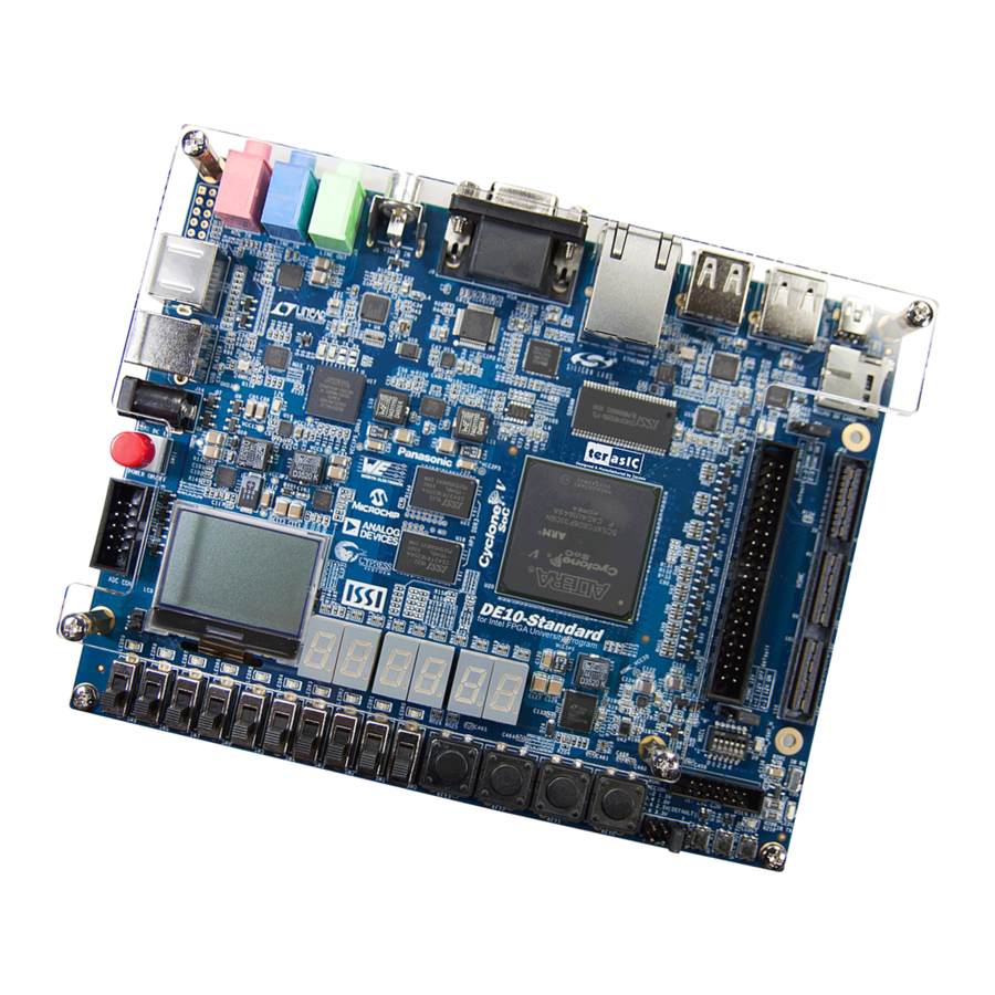
This chapter provides an introduction to the features and design characteristics of the board. Figure 2-1 shows a photograph of the board. It depicts the layout of the board and indicates the location of the connectors and key components. Figure 2-1 DE10-Standard development board (top view) DE10-Standard www.terasic.com User Manual... - Page 9 Figure 2-2 DE10-Standard development board (bottom view) The DE10-Standard board has many features that allow users to implement a wide range of designed circuits, from simple circuits to various multimedia projects. The following hardware is provided on the board: FPGA ...
-
Page 10: Block Diagram Of The De10-Standard Board
All the connections are established through the Cyclone V SoC FPGA device to provide maximum flexibility for users. Users can configure the FPGA to implement any system design. DE10-Standard www.terasic.com User Manual January 19, 2017... - Page 11 Figure 2-3 Block diagram of DE10-Standard Detailed information about Figure 2-3 are listed below. Cyclone V SoC 5CSXFC6D6F31C6N Device Dual-core ARM Cortex-A9 (HPS) 110K programmable logic elements 5,140 Kbits embedded memory 6 fractional PLLs 2 hard memory controllers ...
- Page 12 128x64 dots LCD Module with Backlight 24-bit CODEC, Line-in, Line-out, and microphone-in jacks TV decoder (NTSC/PAL/SECAM) and TV-in connector Interface: SPI Fast throughput rate: 500 KSPS Channel number: 8 Resolution: 12-bit DE10-Standard www.terasic.com User Manual January 19, 2017...
- Page 13 10 user switches (FPGA x10) 11 user LEDs (FPGA x10, HPS x 1) 2 HPS reset buttons (HPS_RESET_n and HPS_WARM_RST_n) Six 7-segment displays G-Sensor on HPS 12V DC input DE10-Standard www.terasic.com User Manual January 19, 2017...
-
Page 14: Chapter 3 Using The De10-Standard Board
This chapter provides an instruction to use the board and describes the peripherals. When the DE10-Standard board is powered on, the FPGA can be configured from EPCS or HPS. The MSEL[4:0] pins are used to select the configuration scheme. It is implemented as a 6-pin DIP... -
Page 15: Configuration Of Cyclone V Soc Fpga On De10-Standard
The information is retained within EPCS128 even if the DE10-Standard board is turned off. When the board is powered on, the configuration data in the EPCS128 device is automatically loaded into the Cyclone V SoC FPGA. - Page 16 JTAG chain must form a closed loop, which allows Quartus II programmer to the detect FPGA device. Figure 3-2 illustrates the JTAG chain on DE10-Standard board. Figure 3-2 Path of the JTAG chain Configure the FPGA in JTAG Mode There are two devices (FPGA and HPS) on the JTAG chain.
- Page 17 Figure 3-3 Detect FPGA device in JTAG mode 2. Select detected device associated with the board, as circled in Figure 3-4. Figure 3-4 Select 5CSXFC6D6 device 3. Both FPGA and HPS are detected, as shown in Figure 3-5. DE10-Standard www.terasic.com User Manual January 19, 2017...
- Page 18 Figure 3-5 FPGA and HPS detected in Quartus programmer 4. Right click on the FPGA device and open the .sof file to be programmed, as highlighted in Figure 3-6. DE10-Standard www.terasic.com User Manual January 19, 2017...
- Page 19 Figure 3-6 Open the .sof file to be programmed into the FPGA device 5. Select the .sof file to be programmed, as shown in Figure 3-7. Figure 3-7 Select the .sof file to be programmed into the FPGA device DE10-Standard www.terasic.com User Manual January 19, 2017...
- Page 20 Figure 3-8 Program .sof file into the FPGA device Configure the FPGA in AS Mode The DE10-Standard board uses a quad serial configuration device (EPCS128) to store configuration data for the Cyclone V SoC FPGA. This configuration data is automatically loaded from the quad serial configuration device chip into the FPGA when the board is powered up.
-
Page 21: Board Status Elements
In addition to the 10 LEDs that FPGA device can control, there are 5 indicators which can indicate the board status (See ), please refer the details in Table 3-3 Figure 3-10 Figure 3-10 LED Indicators on DE10-Standard Table 3-3 LED Indicators Board Reference LED Name Description DE10-Standard www.terasic.com... -
Page 22: Board Reset Elements
UART TXD Illuminate when data is transferred from FT232R to USB Host. UART RXD Illuminate when data is transferred from USB Host to FT232R. JTAG_RX Reserved JTAG_TX There are two HPS reset buttons on DE10-Standard, HPS (cold) reset and HPS warm reset, as shown in Figure 3-11. Table 3-4 describes the purpose of these two HPS reset buttons. -
Page 23: Clock Circuitry
KEY7 HPS_WARM_RST_N system reset domain for debug purpose. Figure 3-12 HPS reset tree on DE10-Standard board Figure 3-13 shows the default frequency of all external clocks to the Cyclone V SoC FPGA. A clock generator is used to distribute clock signals with low jitter. The four 50MHz clock signals connected to the FPGA are used as clock sources for user logic. -
Page 24: Peripherals Connected To The Fpga
Figure 3-13 Block diagram of the clock distribution on DE10-Standard Table 3-5 Pin Assignment of Clock Inputs Signal Name FPGA Pin No. Description I/O Standard CLOCK_50 PIN_AF14 50 MHz clock input 3.3V CLOCK2_50 PIN_AA16 50 MHz clock input 3.3V CLOCK3_50... - Page 25 FPGA. When the switch is set to the DOWN position (towards the edge of the board), it generates a low logic level to the FPGA. When the switch is set to the UP position, a high logic level is generated to the FPGA DE10-Standard www.terasic.com User Manual...
- Page 26 LED on or off, respectively. Figure 3-17 shows the connections between LEDs and Cyclone V SoC FPGA. Table 3-6, Table 3-7 Table 3-8 list the pin assignment of user push-buttons, switches, and LEDs. DE10-Standard www.terasic.com User Manual January 19, 2017...
- Page 27 Push-button[0] 3.3V KEY[1] PIN_AK4 Push-button[1] 3.3V KEY[2] PIN_AA14 Push-button[2] 3.3V KEY[3] PIN_AA15 Push-button[3] 3.3V Table 3-8 Pin Assignment of LEDs Signal Name FPGA Pin No. Description I/O Standard LEDR[0] PIN_AA24 LED [0] 3.3V DE10-Standard www.terasic.com User Manual January 19, 2017...
-
Page 28: 7-Segment Displays
LED [9] 3.3V 3.6.2 7-segment Displays The DE10-Standard board has six 7-segment displays. These displays are paired to display numbers in various sizes. Figure 3-18 shows the connection of seven segments (common anode) to pins on Cyclone V SoC FPGA. The segment can be turned on or off by applying a low logic level or high logic level from the FPGA, respectively. -
Page 29: 2X20 Gpio Expansion Header
Cyclone V SoC FPGA. It also comes with DC +5V (VCC5), DC +3.3V (VCC3P3), and two GND pins. The maximum power consumption allowed for a daughter card connected to one GPIO ports is shown in Table 3-10. DE10-Standard www.terasic.com User Manual January 19, 2017... - Page 30 GPIO Connection 0[12] 3.3V GPIO[13] PIN_AG5 GPIO Connection 0[13] 3.3V GPIO[14] PIN_AG6 GPIO Connection 0[14] 3.3V GPIO[15] PIN_AG7 GPIO Connection 0[15] 3.3V GPIO[16] PIN_AG8 GPIO Connection 0[16] 3.3V GPIO[17] PIN_AF4 GPIO Connection 0[17] 3.3V DE10-Standard www.terasic.com User Manual January 19, 2017...
-
Page 31: Hsmc Connector
The HSMC interface support JTAG, clock outputs and inputs, high-speed serial I/O (transceivers), and single-ended or differential signaling. Signals on the HSMC port are shown in Figure Table 3-12 shows the maximum power consumption of the daughter card that connects to HSMC port. DE10-Standard www.terasic.com User Manual January 19, 2017... - Page 32 Short Pins 3 and 4 1.8V 1.8V Short Pins 5 and 6 2.5V 2.5V (Default) Short Pins 7 and 8 3.3V 3.3V Table 3-13 Pin Assignments for HSMC connector Signal Name FPGA Pin No. Description I/O Standard DE10-Standard www.terasic.com User Manual January 19, 2017...
- Page 33 LVDS RX bit 3 or CMOS I/O Depend on JP3 HSMC_RX_D_P[4] PIN_K7 LVDS RX bit 4 or CMOS I/O Depend on JP3 HSMC_RX_D_P[5] PIN_J7 LVDS RX bit 5 or CMOS I/O Depend on JP3 DE10-Standard www.terasic.com User Manual January 19, 2017...
- Page 34 LVDS TX bit 14 or CMOS I/O Depend on JP3 HSMC_TX_D_P[15] PIN_C12 LVDS TX bit 15 or CMOS I/O Depend on JP3 HSMC_TX_D_P[16] PIN_B13 LVDS TX bit 16 or CMOS I/O Depend on JP3 DE10-Standard www.terasic.com User Manual January 19, 2017...
-
Page 35: 24-Bit Audio Codec
I2C Data 3.3V 3.6.6 I2C Multiplexer The DE10-Standard board implements an I2C multiplexer for HPS to access the I2C bus originally owned by FPGA. Figure 3-21 shows the connection of I2C multiplexer to the FPGA and HPS. HPS can access Audio CODEC and TV Decoder if and only if the HPS_I2C_CONTROL signal is set to DE10-Standard www.terasic.com... -
Page 36: Vga Output
3.6.7 VGA Output The DE10-Standard board has a 15-pin D-SUB connector populated for VGA output. The VGA synchronization signals are generated directly from the Cyclone V SoC FPGA, and the Analog Devices ADV7123 triple 10-bit high-speed video DAC (only the higher 8-bits are used) transforms signals from digital to analog to represent three fundamental colors (red, green, and blue). - Page 37 More information about the ADV7123 video DAC is available in its datasheet, which can be found on the manufacturer’s website, or in the directory \Datasheets\VIDEO DAC of DE10-Standard System CD. The pin assignment between the Cyclone V SoC FPGA and the ADV7123 is listed in Table 3-18.
- Page 38 Table 3-17 VGA Vertical Timing Specification VGA mode Vertical Timing Spec Configuration Resolution(HxV) a(lines) b(lines) c(lines) d(lines) Pixel clock(MHz) VGA(60Hz) 640x480 VGA(85Hz) 640x480 SVGA(60Hz) 800x600 SVGA(75Hz) 800x600 SVGA(85Hz) 800x600 XGA(60Hz) 1024x768 XGA(70Hz) 1024x768 XGA(85Hz) 1024x768 1280x1024(60Hz) 1280x1024 1024 DE10-Standard www.terasic.com User Manual January 19, 2017...
-
Page 39: Tv Decoder
3.6.8 TV Decoder The DE10-Standard board is equipped with an Analog Device ADV7180 TV decoder chip. The ADV7180 is an integrated video decoder which automatically detects and converts a standard analog baseband television signals (NTSC, PAL, and SECAM) into 4:2:2 component video data, which is compatible with the 8-bit ITU-R BT.656 interface standard. - Page 40 Table 3-. More information about the ADV7180 is available on the manufacturer’s website, or in the directory \DE1_SOC_datasheets\Video Decoder of DE10-Standard System CD. Figure 3-24 Connections between the FPGA and TV Decoder Table 3-20 Pin Assignment of TV Decoder Signal Name FPGA Pin No.
-
Page 41: Ir Receiver
The board comes with an infrared remote-control receiver module (model: IRM-V538/TR1), whose datasheet is provided in the directory \Datasheets\ IR Receiver and Emitter of DE10-Standard system CD. The remote control, which is optional and can be ordered from the website, has an encoding chip (uPD6121G) built-in for generating infrared signals. -
Page 42: Sdram Memory
16-bit data line, control line, and address line connected to the FPGA. This chip uses the 3.3V LVCMOS signaling standard. Connections between the FPGA and SDRAM are shown in Figure 3-27, and the pin assignment is listed in Table 3-19. DE10-Standard www.terasic.com User Manual January 19, 2017... - Page 43 SDRAM Data[4] 3.3V DRAM_DQ[5] PIN_AG10 SDRAM Data[5] 3.3V DRAM_DQ[6] PIN_AK11 SDRAM Data[6] 3.3V DRAM_DQ[7] PIN_AJ11 SDRAM Data[7] 3.3V DRAM_DQ[8] PIN_AH10 SDRAM Data[8] 3.3V DRAM_DQ[9] PIN_AJ10 SDRAM Data[9] 3.3V DRAM_DQ[10] PIN_AJ9 SDRAM Data[10] 3.3V DE10-Standard www.terasic.com User Manual January 19, 2017...
-
Page 44: Ps/2 Serial Port
SDRAM Chip Select 3.3V 3.6.12 PS/2 Serial Port The DE10-Standard board comes with a standard PS/2 interface and a connector for a PS/2 keyboard or mouse. Figure 3-28 shows the connection of PS/2 circuit to the FPGA. Users can use... -
Page 45: A/D Converter And 2X5 Header
PS/2 Clock (reserved for second PS/2 device) 3.3V PS2_DAT2 PIN_AB26 PS/2 Data (reserved for second PS/2 device) 3.3V 3.6.13 A/D Converter and 2x5 Header The DE10-Standard has an analog-to-digital converter (LTC2308), which features low noise, DE10-Standard www.terasic.com User Manual January 19, 2017... - Page 46 Figure 3-29. More information about the A/D converter chip is available in its datasheet. It can be found on manufacturer’s website or in the directory \datasheet of DE10-Standard system CD. Figure 3-29 Signals of the 2x5 Header Figure 3-30 shows the connections between the FPGA, 2x5 header, and the A/D converter.
-
Page 47: Peripherals Connected To Hard Processor System (Hps)
The pin assignment associated to Gigabit Ethernet interface is listed in Table 3-23. More information about the KSZ9021RN PHY chip and its datasheet, as well as the application notes, which are available on the manufacturer’s website. DE10-Standard www.terasic.com User Manual January 19, 2017... - Page 48 3-24. For instance, the connection from board to Gigabit Ethernet is established once the LEDG lights on. Table 3-24 State and Definition of LED Mode Pins LED (State) LED (Definition) Link /Activity LEDG LEDY LEDG LEDY DE10-Standard www.terasic.com User Manual January 19, 2017...
-
Page 49: Uart To Usb
FT232R chip to the host with an USB Mini-B connector. More information about the chip is available on the manufacturer’s website, or in the directory \Datasheets\UART TO USB of DE10-Standard system CD. Figure 3-32 shows the connections between the HPS, FT232R chip, and the USB Mini-B connector. -
Page 50: Ddr3 Memory
SSTL-15 Class I HPS_DDR3_DQ[2] PIN_H30 HPS DDR3 Data[2] SSTL-15 Class I HPS_DDR3_DQ[3] PIN_G28 HPS DDR3 Data[3] SSTL-15 Class I HPS_DDR3_DQ[4] PIN_L25 HPS DDR3 Data[4] SSTL-15 Class I HPS_DDR3_DQ[5] PIN_L24 HPS DDR3 Data[5] SSTL-15 Class I DE10-Standard www.terasic.com User Manual January 19, 2017... - Page 51 PIN_D30 DDR3 Row Address Strobe SSTL-15 Class I HPS_DDR3_RESET_n PIN_P30 HPS DDR3 Reset SSTL-15 Class I HPS_DDR3_WE_n PIN_C28 HPS DDR3 Write Enable SSTL-15 Class I HPS_DDR3_RZQ PIN_D27 External reference ball for 1.5 V DE10-Standard www.terasic.com User Manual January 19, 2017...
-
Page 52: Micro Sd Card Socket
The board supports Micro SD card interface with x4 data lines. It serves not only an external storage for the HPS, but also an alternative boot option for DE10-Standard board. Figure 3-33 shows signals connected between the HPS and Micro SD card socket. -
Page 53: Accelerometer (G-Sensor)
I2C interface. The I2C address of G-sensor is 0xA6/0xA7. More information about this chip can be found in its datasheet, which is available on manufacturer’s website or in the directory \Datasheet folder of DE10-Standard system CD. Figure 3-35 shows the connections between the HPS and G-sensor. -
Page 54: Ltc Connector
GPIO, SPI, or I2C based communication with the HPS. Connections between the HPS and LTC connector are shown in Figure 3-36, and the pin assignment of LTC connector is listed in Table 3-27. DE10-Standard www.terasic.com User Manual January 19, 2017... -
Page 55: 128X64 Dots Lcd
HPS and LCD module. The default setting for LCD backlight power is ON by shorting the pins of header JP4. Table 3-28 lists the pin assignments between LCD module and Cyclone V SoC FPGA. DE10-Standard www.terasic.com User Manual January 19, 2017... - Page 56 PIN_C18 HPS LCM Data bit is Data/Command 3.3V HPS_LCM_RST_N PIN_E17 HPS LCM Reset 3.3V HPS_LCM_SPIM_CLK PIN_A23 SPI Clock 3.3V HPS_LCM_SPIM_MOSI PIN_C22 SPI Master Output /Slave Input 3.3V HPS_LCM_SPIM_SS PIN_H20 SPI Slave Select 3.3V DE10-Standard www.terasic.com User Manual January 19, 2017...
-
Page 57: Chapter 4 De10-Standard System Builder
This chapter describes how users can create a custom design project with the tool named DE10-Standard System Builder. The DE10-Standard System Builder is a Windows-based utility. It is designed to help users create a Quartus II project for DE10-Standard within minutes. The generated Quartus II project files include: ... -
Page 58: Using De10-Standard System Builder
The DE10-Standard System Builder will generate two major files, a top-level design file (.v) and a Quartus II setting file (.qsf) after users launch the DE10-Standard System Builder and create a new project according to their design requirements The top-level design file contains a top-level Verilog HDL wrapper for users to add their own design/logic. - Page 59 The DE10-Standard System Builder is located in the directory: “Tools\SystemBuilder” of the DE10-Standard System CD. Users can copy the entire folder to a host computer without installing the utility. A window will pop up, as shown in Figure 4-2, after executing the DE10-Standard SystemBuilder.exe on the host computer.
-
Page 60: System Configuration
Figure 4-4. Each component onboard is listed and users can enable or disable one or more components at will. If a component is enabled, the DE10-Standard System Builder will automatically generate its associated pin assignment, including the pin name, pin location, pin direction, and I/O standard. - Page 61 Figure 4-4 System configuration group GPIO and HSMC Expansion If users connect any Terasic GPIO-based or HSMC-based daughter cards to the GPIO connector or HSMC connector on DE10-Standard, the DE10-Standard System Builder can generate a project that include the corresponding module, as shown in Figure 4-5.
- Page 62 The “Prefix Name” is an optional feature that denote the pin name of the daughter card assigned in your design. Users may leave this field blank. Project Setting Management The DE10-Standard System Builder also provides the option to load a setting or save users’ current board configuration in .cfg file, as shown in Figure 4-6.
- Page 63 Figure 4-6 Project Settings Project Generation When users press the Generate button, the DE10-Standard System Builder will generate the corresponding Quartus II files and documents, as listed in Table 4-1: Table 4-1 Files generated by the DE10-Standard System Builder...
-
Page 64: Examples For Fpga
Project directory: DE10_Standard_Default Bitstream used: DE10_Standard_Default.sof or DE10_Standard_Default.jic Power on the DE10-Standard board with the USB cable connected to the USB-Blaster II port. If necessary (that is, if the default factory configuration is not currently stored in the EPCS device), download the bit stream to the board via JTAG interface. -
Page 65: Audio Recording And Playing
Figure 5-1 Command line of the batch file to program the FPGA and EPCS device This demonstration shows how to implement an audio recorder and player on DE10-Standard board with the built-in audio CODEC chip. It is developed based on Qsys and Eclipse. - Page 66 Connect a speaker or headset to the Line-out port Load the bitstream into the FPGA. (note *1) Load the software execution file into the FPGA. (note *1) Configure the audio with SW0, as shown in Table 5-1. DE10-Standard www.terasic.com User Manual January 19, 2017...
-
Page 67: Karaoke Machine
(2). Recording process will stop if the audio buffer is full. (3). Playing process will stop if the audio data is played completely. This demonstration uses the microphone-in, line-in, and line-out ports on DE10-Standard to create a Karaoke machine. The WM8731 CODEC is configured in master mode. The audio CODEC generates AD/DA serial bit clock (BCK) and the left/right channel clock (LRCK) automatically. - Page 68 Users should be able to hear a mixture of microphone sound and the sound from the music player Press KEY0 to adjust the volume; it cycles between volume level 0 to 9 Figure 5-5 illustrates the setup for this demonstration. DE10-Standard www.terasic.com User Manual January 19, 2017...
-
Page 69: Sdram Test In Nios Ii
The SDRAM controller is configured as a 64MB controller. The working frequency of the SDRAM controller is 100MHz, and the Nios II program is running on the on-chip memory. DE10-Standard www.terasic.com User Manual January 19, 2017... - Page 70 Design Tools Quartus II v16.1 Nios II Eclipse v16.1 Demonstration Source Code Quartus project directory: SDRAM_Nios_Test Nios II Eclipse directory: SDRAM_Nios_Test \Software Nios II Project Compilation DE10-Standard www.terasic.com User Manual January 19, 2017...
- Page 71 Press any button (KEY3~KEY0) to start the SDRAM verification process. Press KEY0 to run the test continuously. The program will display the test progress and result, as shown in Figure 5-7. DE10-Standard www.terasic.com User Manual January 19, 2017...
-
Page 72: Sdram Test In Verilog
Figure 5-7 Display of progress and result for the SDRAM test in Nios II DE10-Standard system CD offers another SDRAM test with its test code written in Verilog HDL. The memory size of the SDRAM bank tested is still 64MB. - Page 73 If LEDR1 failed to remain ON after approximately 8 seconds, the SDRAM test is NG. Press KEY0 again to repeat the SDRAM test. Table 5-3 Status of LED Indicators Name Description LEDR0 Reset LEDR1 ON if the test is PASS after releasing KEY0 DE10-Standard www.terasic.com User Manual January 19, 2017...
-
Page 74: Tv Box Demonstration
LEDR2 Blinks This demonstration turns DE10-Standard board into a TV box by playing video and audio from a DVD player using the VGA output, audio CODEC and the TV decoder on the DE10-Standard board. Figure 5-9 shows the block diagram of the design. There are two major blocks in the system called I2C_AV_Config and TV_to_VGA. - Page 75 Connect the VGA output of the DE10_Standard board to a VGA monitor. Connect the audio output of the DVD player to the line-in port of the DE10_Standard board and connect a speaker to the line-out port. If the audio output jacks from the DVD player are DE10-Standard www.terasic.com User Manual...
-
Page 76: Ps/2 Mouse Demonstration
Introduction PS/2 protocol uses two wires for bi-directional communication. One is the clock line and the other one is the data line. The PS/2 controller always has total control over the transmission line, but it is DE10-Standard www.terasic.com User Manual... - Page 77 After the power on cycle of the PS/2 mouse, it enters into stream mode automatically and disable data transmit unless an enabling instruction is received. Figure 5-11 shows the waveform while communication happening on two lines. DE10-Standard www.terasic.com User Manual January 19, 2017...
- Page 78 Project directory: DE10_Standard _PS2 Bitstream used: DE10_Standard _PS2.sof Demo batch file directoy: \DE10_Standard _PS2 \demo_batch The folder includes the following files: Batch file:test.bat FPGA configuration file : DE10_Standard _PS2.sof DE10-Standard www.terasic.com User Manual January 19, 2017...
-
Page 79: Ir Emitter Led And Receiver Demonstration
It implements a IR TX Controller and a IR RX Controller. When KEY0 is pressed, data test pattern generator will generate data to the IR TX Controller continuously. When IR TX Controller is active, it will format the data to be compatible DE10-Standard www.terasic.com User Manual... - Page 80 4.5ms window. The second inversed data is sent to verify the accuracy of the information received. A final 562.5µs pulse burst is sent to signify the end of message transmission. Because the data is sent in pair (original and inverted) according to the protocol, the overall DE10-Standard www.terasic.com User Manual...
- Page 81 The last bit end code represents the end of the frame. The value of this frame is completely inverted at the receiving end. Figure 5-15 The remote control used in this demonstration DE10-Standard www.terasic.com User Manual...
- Page 82 GUIDANCE to DATAREAD state. The Code Detector will also save the receiving data and output to the Shift Register and display on the 7-segment. Figure 5-18 shows the state shift diagram of State Machine block. The input clock should be 50MHz. DE10-Standard www.terasic.com User Manual January 19, 2017...
- Page 83 Figure 5-18 State shift diagram of State Machine block Project directory: DE10_Standard_IR Bitstream used: DE10_Standard_IR.sof Demo batch file directory: DE10_Standard_IR \demo_batch The folder includes the following files: Batch file: test.bat FPGA configuration file : DE10_Standard_IR.sof DE10-Standard www.terasic.com User Manual January 19, 2017...
-
Page 84: Adc Reading
The voltage should be adjusted within the range between 0 and 4.096V. The 12-bit voltage measurement is displayed on the NIOS II console. Figure 5-19 shows the block diagram of this demonstration. The default full-scale of ADC is 0~4.096V. DE10-Standard www.terasic.com User Manual January 19, 2017... - Page 85 (SCK) to operate at any frequency up to 40MHz.In this demonstration, we realized the SPI protocol in Verilog, and packet it into Avalon MM slave IP so that it can be connected to Qsys. Figure 5-21 is SPI timing specification of LTC2308. DE10-Standard www.terasic.com User Manual January 19, 2017...
- Page 86 Sample Voltage = ADC Data / full scale Data * Reference Voltage. In this demonstration, full scale is 2^12 =4096. Reference Voltage is 4.096V. Thus ADC Value = ADC data/4096*4.096 = ADC data /1000 DE10-Standard www.terasic.com User Manual January 19, 2017...
- Page 87 Software project directory: DE10_Standard _ADC software Demo batch file : DE10_Standard _ADC\demo_batch\ DE10_Standard _ADC.bat Demonstration Setup and Instructions Connect the trimmer to corresponding ADC channel on the 2x5 header, as shown in Figure DE10-Standard www.terasic.com User Manual January 19, 2017...
- Page 88 The Nios II console will display the voltage of the specified channel voltage result information. Provide any input voltage to other ADC channels and set SW[2:0] to the corresponding channel if user want to measure other channels Figure 5-23 Hardware setup for the ADC reading demonstration DE10-Standard www.terasic.com User Manual January 19, 2017...
-
Page 89: Examples For Hps Soc
This chapter provides several C-code examples based on the Altera SoC Linux built by Yocto project. These examples demonstrates major features connected to HPS interface on DE10-Standard board such as users LED/KEY, I2C interfaced G-sensor, and I2C MUX. All the associated files can be found in the directory Demonstrations/SOC of the DE10_Standard System CD. - Page 90 The "make" command will build the project. The executable file "my_first_hps" will be generated after the compiling process is successful. The "clean all" command removes all temporary files. Demonstration Source Code Build tool: SoC EDS v16.1 DE10-Standard www.terasic.com User Manual January 19, 2017...
-
Page 91: Users Led And Key
GPIO1 controller in HPS. The behavior of GPIO controller is controlled by the register in GPIO controller. The registers can be accessed by application software through the memory-mapped device driver, which is built into Altera SoC Linux. DE10-Standard www.terasic.com User Manual... - Page 92 GPIO1 controller. GPIO[70..58] and input-only GPI[13..0] are controlled by the GPIO2 controller. Figure 6-2 Block diagram of GPIO Interface GPIO Register Block The behavior of I/O pin is controlled by the registers in the register block. There are three 32-bit DE10-Standard www.terasic.com User Manual January 19, 2017...
- Page 93 The registers of the GPIO1 controller are mapped to the base address 0xFF708000 with 4KB size, and the registers of the GPIO2 controller are mapped to the base address 0xFF70A000 with 4KB size, as shown in Figure 6-3. DE10-Standard www.terasic.com User Manual January 19, 2017...
- Page 94 alt_clrbits_word: set specified bit value to zero for a specified register The program must include the following header files to use the above API to access the registers of GPIO controller. #include <stdio.h> #include <unistd.h> #include <fcntl.h> #include <sys/mman.h> #include "hwlib.h" DE10-Standard www.terasic.com User Manual January 19, 2017...
- Page 95 GPIO1 controller. The status of KEY can be queried by reading the value of the bit-24 in the gpio_ext_porta register of the GPIO1 controller. gpio_swporta_ddr Figure 6-5 register in the GPIO1 controller The following mask is defined in the demo code to control LED and KEY direction and LED’s DE10-Standard www.terasic.com User Manual January 19, 2017...
- Page 96 Insert the booting micro SD card into the DE10_Standard board. Power on the DE10_Standard board. Launch PuTTY and establish connection to the UART port of Putty. Type "root" to login Altera DE10-Standard www.terasic.com User Manual January 19, 2017...
-
Page 97: I2C Interfaced G-Sensor
PIO controller. This demonstration uses polling method to read the register data. Figure 6-6 Block diagram of the G-sensor demonstration I2C Driver The procedures to read a register value from G-sensor register files by the existing I2C bus driver in DE10-Standard www.terasic.com User Manual January 19, 2017... - Page 98 DATA_FORAMT(0x31) register. The data format in this demonstration is configured as: Full resolution mode ± 16g range mode Left-justified mode The X/Y/Z data value can be derived from the DATAX0(0x32), DATAX1(0x33), DATAY0(0x34), DE10-Standard www.terasic.com User Manual January 19, 2017...
-
Page 99: I2C Mux Test
Figure 6-8. Figure 6-8 Terminal output of the G-sensor demonstration Press "CTRL + C" to terminate the program. The I2C bus on DE10-Standard is originally accessed by FPGA only. This demonstration shows DE10-Standard www.terasic.com User Manual January 19, 2017... - Page 100 The following statement is used to set HPS_I2C_CONTROL high. alt_setbits_word( ( virtual_base + ( ( uint32_t )( ALT_GPIO1_SWPORTA_DR_ADDR ) & ( uint32_t )( HW_REGS_MASK ) ) ), HPS_I2C_CONTROL The following statement is used to set HPS_I2C_CONTROL low. DE10-Standard www.terasic.com User Manual January 19, 2017...
- Page 101 Execute "./ i2c_switch " in the UART terminal of PuTTY to start the I2C MUX test. The demo program will show the result in the Putty, as shown in Figure 6-10. Figure 6-10 Terminal output of the I2C MUX Test Demonstration DE10-Standard www.terasic.com User Manual January 19, 2017...
-
Page 102: Spi Interfaced Graphic Lcd
The LCD is connected to the SPIM0, GPIO1 controller in HPS on this DE10-Standard board. The built-in virtual memory-mapped device driver in the system is used to access the registers in the HPS SPIM and GPIO controllers. - Page 103 LCD. It then calls "LCDHW_BackLight" to turn on the backlight of LCD. "LCD_Init" is called to initialize LCD configuration. Finally, the APIs in lcd_graphic.c are called to draw graphic on the LCD. DE10-Standard www.terasic.com User Manual...
- Page 104 Power on the DE10-Standard t board. Launch PuTTY to connect to the UART port of DE10-Standard board and type "root" to login Yocto Linux. In the UART terminal of PuTTY, type "./hps_lcd" to start the LCD demo, as shown in Figure 6-13.
- Page 105 Figure 6-14 LCD display for the LCD Demonstration DE10-Standard www.terasic.com User Manual January 19, 2017...
-
Page 106: Examples For Using Both Hps Soc And Fgpa
Basic SoC EDS(Embedded Design Suite) operation skill Basic C coding and compiling skill Skill to Create a Linux Boot SD-Card for DE10-Standard with a given image file Skill to boot Linux from SD-Card on DE10-Standard Skill to cope files into Linux... -
Page 107: System Requirements
Before starting this tutorial, please note that the following items are required to complete the demonstration project: Terasic DE10-Standard FPGA board, includes Mini USB Cable for UART terminal Micros SD-Card, at 4GB minimum Micros SD-Card Card Reader ... -
Page 108: Ghrd Project
HPS-to-FPGA bridge. This Demo introduces to users how to use the HPS/ARM to communicate with FPGA. This project includes GHRD project for the DE10-Standard one ARM C Project which demonstrates how HPS/ARM program controls the ten LEDs connected to FPGA. - Page 109 Quartus II Software. Then open the soc_system.qsys file with the Qsys tool. Figure 7-2 lists the address map of the peripherals which are connected to the lightweight HPS-to-FPGA. Figure 7-2 FPGA peripherals address map DE10-Standard www.terasic.com User Manual January 19, 2017...
-
Page 110: Compile And Programming
All the Avalon Conduit signals of these peripherals are connected to the I/O pins of the SoCFPGA on DE10-Standard board as shown in the Figure 7-3. Figure 7-3 Connection in the top design In the Qsys tool, click the menu item “GenerateGenerate…” to generate source code for the system and then close the Qsys tool. -
Page 111: Develop The C Code
DE10_Standard_SoC_GHRD.sof is generated in the DE10_Standard_SoC_GHRD\output_files folder. Users can use this file to configure FPGA by Quartus Programming through the DE10-Standard on-board USB-Blaster II. This section introduces how to design an ARM C program to control the led_pio PIO controller. - Page 112 Offset address of Pio_led relative to Lightweight HPS-to-FPGA AXI bus first offset address 0xff200000 which defined constant ALT_LWFPGASLVS_OFST in the header hps.h. The hps.h is a header of SoC EDS. It is located in the Quartus installation folder: DE10-Standard www.terasic.com User Manual January 19, 2017...
-
Page 113: Led Control
DE10-Standard is high active, writing a value 0x00000000 to the offset 0 register will turn off all of the nine red LEDs. There are 10 red LEDs on DE10-Standard and 9 of them are connected to this controller. The last LED (LED0) is used to implement FPGA heartbeat. Writing a value 0x000001ff to the offset 0 register will turn on all of nine red LEDs. - Page 114 Makefile and compile Figure 7-9 shows the content of Makefile for this C project. The program includes the head files provided by SoC EDS. In the Makefile, ARM-linux cross-compile also be specified. DE10-Standard www.terasic.com User Manual January 19, 2017...
- Page 115 Figure 7-10 ARM C Project Compilation Execute the Demo To execute the demo, please boot the Linux from the SD-card in DE10-Standard. Copy the execution file “HPS_FPGA_LED” to the Linux directory, and type “chmod +x HPS_FPGA_LED” to add execution attribute to the execute file. Use Quartus Programmer to configure FPGA with the DE10_NANO_SoC_GHRD.sof generated in previous chapter.
- Page 116 The LED0 will flash as the heat beat of the FPGA. Then, type “./ HPS_FPGA_LED” to launch the ARM program. The LED[9..1] on DE10-Standard I will be expected to perform 60 times of LED light shift operation, and then the program is terminated.
-
Page 117: Programming The Epcs Device
The FPGA should be set to AS x1 mode i.e. MSEL[4..0] = “10010” to use the quad Flash as a FPGA configuration device. 1. Choose Convert Programming Files from the File menu of Quartus II, as shown in Figure 8-1. DE10-Standard www.terasic.com User Manual January 19, 2017... - Page 118 5. Browse to the target directory from the File name field and specify the name of output file. 6. Click on the SOF data in the section of Input files to convert, as shown in Figure 8-2. DE10-Standard www.terasic.com User Manual January 19, 2017...
- Page 119 8. Select the .sof to be converted to a .jic file from the Open File dialog. 9. Click Open. 10. Click on the Flash Loader and click Add Device, as shown in Figure 8-3. 11. Click OK and the Select Devices page will appear. DE10-Standard www.terasic.com User Manual January 19, 2017...
- Page 120 12. Select the targeted FPGA to be programed into the EPCS, as shown in Figure 8-4. 13. Click OK and the Convert Programming Files page will appear, as shown in Figure 8-5. 14. Click Generate. DE10-Standard www.terasic.com User Manual January 19, 2017...
- Page 121 Figure 8-4 “Select Devices” page DE10-Standard www.terasic.com User Manual January 19, 2017...
-
Page 122: Write Jic File Into The Epcs Device
Figure 8-6. 4. Double click the green rectangle region shown in Figure 8-6 and the Select New Programming File page will appear. Select the .jic file to be programmed. DE10-Standard www.terasic.com User Manual January 19, 2017... - Page 123 5. Program the EPCS device by clicking the corresponding Program/Configure box. A factory default SFL image will be loaded, as shown in Figure 8-7. 6. Click Start to program the EPCS device. Figure 8-6 Two devices are detected in the Quartus II Programmer DE10-Standard www.terasic.com User Manual January 19, 2017...
-
Page 124: Erase The Epcs Device
4. Double click the green rectangle region shown in Figure 8-6, and the Select New Programming File page will appear. Select the correct .jic file. 5. Erase the EPCS device by clicking the corresponding Erase box. A factory default SFL DE10-Standard www.terasic.com User Manual January 19, 2017... - Page 125 Figure 8-8. Figure 8-8 Erase the EPCS device in Quartus II Programmer 6. Click Start to erase the EPCS device. DE10-Standard www.terasic.com User Manual January 19, 2017...
-
Page 126: Chapter 9 Appendix
Chapter 9 Appendix Version Change Log V0.1 Initial Version (Preliminary) Copyright © 2017 Terasic Technologies. All rights reserved. DE10-Standard www.terasic.com User Manual January 19, 2017...
Need help?
Do you have a question about the DE10-Standard and is the answer not in the manual?
Questions and answers