Table of Contents
Advertisement
Quick Links
Advertisement
Table of Contents

Related Manuals for Terasic Altera DE3


Summary of Contents for Terasic Altera DE3
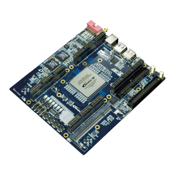
- Page 1 Altera DE3 Board...
-
Page 2: Table Of Contents
Using DE3 System Builder ....................43 Creating My First DE3 Project ..................49 Connect TERASIC Daughter Boards to a DE3 Board ............50 Connect Multiple DE3 Boards ................... 53 Connect a Custom-Made Daughter Board to the DE3 Board ..........56... - Page 3 Altera DE3 Board Chapter 5 Examples of Advanced Demonstration ................ 58 USB Host ........................... 58 USB Device........................65 SD Card ..........................68 DDR2 SDRAM ........................73 Appendix A Pin connections between components and FPGA on the DE3 board ..... 80 Appendix B Pin Compatible List for HSTC and HSMC Connector ..........
-
Page 4: Chapter 1 Overview
DE3 boards into a powerful system as shown in Figure 1.1. The DE3 can also connect with multiple daughter boards designed by Terasic in stock. Figure 1.1 The stackable mechanism of the DE3 board 1.2 Layout and Components Figure 1.2 Figure 1.3... - Page 5 DE3 User Manual USB Device SMA External Clock In Power ON/OFF Switch Power Supply USB Blaster USB Device USB Host/Device SMA PLL Clock Out Connector Expansion Header 2 USB Host/Device Expansion Header 1 Controller Altera USB Blaster HSTC Connector A Controller Chipset HSTC Connector D HSTC Bottom Side...
- Page 6 DE3 User Manual HSTC connector D HSTC connector A HSTC connector B Temperature Sensor HSTC connector C SD Card Slot Figure 1.3. The DE3 board (Bottom view) The following hardware is implemented on the DE3 board: • Altera Stratix III FPGA device (3SL340/3SE260/3SL150) ®...
-
Page 7: Block Diagram Of The De3 Board
DE3 User Manual • User I/O Interface: 4 push-button switches 4 slide switches 1 eight position DIP switch 2 seven-segment displays 8 RGB LEDs • Clock system One 50MHz oscillator 2 SMA connectors for external clock input and PLL clock output •... - Page 8 DE3 User Manual HOST HOST DEVICE C x2 C x2 Hi-Speed Clock IN x5 Clock IN x5 Clock OUT x5 Clock OUT x5 x120 x120 EPCS128 Stratix III JTAG x4 EPM240 JVC x4 PLL OUT PLL_OUT EP3SL150F1152/ Select and Power ON CLOCK IN EP3SL340F1152/ CLOCK_IN...
- Page 9 DE3 User Manual Below is more detailed information regarding the blocks in Figure 1.4: Stratix III FPGA • EP3SL340 338,000 logic elements (LEs) 18,381K Total Memory Kbits 526 18x18-bit Multipliers blocks 12 phase-locked-loops (PLLs) • EP3SE260 254,400 logic elements (LEs) 16,282K Total Memory Kbits 768 18x18-bit Multipliers blocks 12 phase-locked-loops (PLLs)
- Page 10 • Support Nios II with the Terasic driver • Support Programmed I/O (PIO) and Direct Memory Access (DMA) Eight 180-pin High Speed Terasic Connectors (HSTC) expansion headers • 4 male and 4 female connectors are on the top and the bottom of DE3 board, respectively.
-
Page 11: Chapter 2 Using The De3 Board
This chapter gives instructions for using the DE3 board and its components. It is strongly recommended that users should read the Getting Started with the Altera DE3 board.pdf before using the DE3 board. The document is located in the DE3_usermanual folder on the DE3 System CD. - Page 12 DE3 User Manual Quartus II Programmer JTAG Config Signals USB Blaster Circuit JTAGUART Figure 2.1 The JTAG configuration scheme Programming the serial configuration device : The DE3 board contains a serial configuration device (U4) that stores configuration data for the Stratix III FPGA. This configuration data is automatically loaded from the serial configuration device chip into the FPGA when the board is powered up.
-
Page 13: Jtag Chain
DE3 User Manual 2.2 JTAG Chain This section describes how to setup the JTAG chain on DE3 board. If the DE3 board is used without any board connected and all the positions in SW6 are switched to OFF (i.e., down position), the JTAG-interface signals of all HSTC connectors are bypassed, as shown in Figure 2.3. - Page 14 DE3 User Manual DE3 Board Statix III FPGA HSTC Connector A Bypassed HSTC Connector B USB Blaster Circuit Bypassed Cable Host HSTC Connector C Bypassed HSTC Connector D Bypassed Figure 2.3. JTAG chain for a standalone DE3 board Daughter Board DE3 Board HSTC Connector Stratix III FPGA...
- Page 15 DE3 User Manual Figure 2.5. The two DE3 boards stacked and the JTAG path is established through HSTC connector DE3 Board 1 HSTC Connector A Bottom Stratix III FPGA Cable Host Blaster Circuit DE3 Board 2 HSTC Connector A Stratix III FPGA Blaster Circuit Figure 2.6.
-
Page 16: Using The User I/O Interface
DE3 User Manual 2.3 Using the User I/O Interface Push-Button Switches: The DE3 board provides four user-defined, one CPU reset, and one Reconfigure push-button switches. The Reconfigure push-button is used to force a re-boot of the FPGA from the serial configuration device. -
Page 17: I/O Groups And
DE3 User Manual blue color, driven directly by the Stratix III FPGA; The LED is turned on or off when the associated pins are driven to a low or high logic level, respectively. A list of the pin names on the FPGA that are connected to the RGB LEDs is given in Table A-4. - Page 18 DE3 User Manual into four I/O groups, named A, B, C and D. Table 2-2 shows the relation between I/O groups and connectors. Table 2-2 The relation between I/O groups and connectors I/O Group Connectors HSTC connector A, GPIO expansion headers HSTC connector B, DDR2 SO-DIMM socket HSTC connector C HSTC connector D...
- Page 19 DE3 User Manual Finally, there are LEDs located at the left-top corner of the DE3 board to indicate the V voltage CCIO level of each I/O group, as shown in Figure 2.11. For example, the LED VA1 and VA2 will be turned on and off, respectively, when the V of I/O Group A is set to 2.5V.
-
Page 20: Using The Hstc Connectors
DE3 User Manual 2.5 Using the HSTC Connectors The High Speed Terasic Connector (HSTC) is a high speed expansion interface defined by Terasic Technologies. The DE3 board is equipped with 8 HSTC connectors (J1 ~ J8), which can be used to connect the Stratix III FPGA with daughter boards or the other DE3 boards. - Page 21 DE3 User Manual VCC33 VCC33 HSTCA_CLKOUT_n0 HSTCA_CLKIN_n0 HSTC_CLKIN_n 0 HSTC_CLKOUT_n0 HSTC_CLKIN_p 0 HSTC_CLKOUT_p0 HSTCA_CLKOUT_p0 HSTCA_CLKIN_p0 HSTC_RX_n0 HSTC_TX_n0 HSTCA_TX_n0 HSTCA_RX_n0 HSTC_RX_p0 HSTCA_RX_p0 HSTC_TX_p0 HSTCA_TX_p0 HSTC_RX_n1 HSTC_TX_n1 HSTCA_TX_n1 HSTCA_RX_n1 HSTC_RX_p1 HSTC_TX_p1 HSTCA_TX_p1 HSTCA_RX_p1 HSTCA_TX_n2 HSTCA_RX_n2 HSTC_RX_n2 HSTC_TX_n2 HSTC_RX_p2 HSTC_TX_p2 HSTCA_TX_p2 HSTCA_RX_p2 Bank HSTC_RX_n3 HSTC_TX_n3 HSTCA_TX_n3...
- Page 22 DE3 User Manual Share the same I/O pins with other connectors: The HSTC connector group HSTCA (J1, J2) and HSTCB (J3, J4) share the same I/O pins with the GPIO expansion headers (J13, J14) and DDR2 SO-DIMM socket (J9), respectively. Hence none of the combinations above is allowed to be used at the same time.
-
Page 23: Connecting Hstc/Hsmc Daughter Boards To De3 Hstc Connectors
DE3 User Manual 2.6 Connecting HSTC/HSMC Daughter Boards to DE3 HSTC connectors It is important when the HSTC/HSMC daughter boards are connected to the DE3 HSTC connector is to ensure the I/O pins are properly matched between the daughter board and the DE3 connector in particular the 12V, 5V, and 3.3V power pins. -
Page 24: Using The Ddr2 So-Dimm
DE3 User Manual GPIO 0 GPIO 1 GPIO0_CLKINn0 GPIO0_D0 GPIO1_CLKINn1 GPIO1_D0 GPIO0_CLKINp0 GPIO1_CLKINp1 GPIO0_D1 GPIO1_D1 GPIO0_D2 GPIO0_D3 GPIO1_D2 GPIO1_D3 GPIO0_D4 GPIO0_D5 GPIO1_D4 GPIO1_D5 GPIO0_D6 GPIO0_D7 GPIO1_D6 GPIO1_D7 GPIO0_D8 GPIO0_D9 GPIO1_D8 GPIO1_D9 GPIO0_D10 GPIO0_D11 GPIO1_D10 GPIO1_D11 GPIO0_D12 GPIO0_D13 GPIO1_D12 GPIO1_D13 GPIO0_CLKOUTn0 GPIO0_D14 GPIO1_CLKOUTn1 GPIO1_D14... -
Page 25: Using The Usb Otg
DE3 User Manual command input signals DDR2_CS_N[1..0] and presence-detect address input signals DDR2_SA[1..0]. Users should never use the DDR2 SO-DIMM socket and the HSTC connector B at the same time. Figure 2.16 shows the connections between the DDR2 SO-DIMM socket and Stratix III device. -
Page 26: Using The Sd Card
DE3 User Manual miniAB See Table A-15 A[ 1..17] See Table A-15 USB_ID D[ 0..31] JP1 Close = Host JP1 Open = Device ISP1761ET TYPE A HC_IRQ DC_IRQ RESET Host HC_DREQ HC_DACK DC_DREQ DC_DACK TYPE A CLKIN Host 12MHz Figure 2.17. Connections between the USB OTG and Stratix III device Detailed information of the ISP1761ET device can be found in its datasheet and programming guide;... -
Page 27: Led Indicators
DE3 User Manual Figure 2.18. Connections between the SD card and Stratix III 2.11 LED Indicators The DE3 board includes some LEDs to indicate the specified hardware status. The relationship of LED names and their associated functions are list in Table 2-5. - Page 28 DE3 User Manual The clock output of Stratix III FPGA includes HSTC connectors, GPIO expansion headers, SMA connector, and SD card socket as shown in Figure 2.19. The associated pin assignments for clock buffer and SMA connectors to FPGA I/O pins are shown Table A-17.
- Page 29 DE3 User Manual Stratix III +3.3V Adjustable CLKOUT_n0 CLKOUT_n0 VCCIO PLL_B1_CLKOUT4 Level CLKOUT_p0 CLKOUT_p0 50MHz PLL_B1_CLKOUT3 CLK4p Shift CLKOUT_n1 CLKOUT_n1 OSC_BA PLL_B1_CLKOUT0n CLKOUT_p1 CLKOUT_p1 PLL_B1_CLKOUT0p CLKIN2 CLK4n Bank 3C CLKIN_n1 CLKIN_n1 CLK5n CLKIN_p1 CLKIN_p1 CLK5p CLKIN_n0 CLKIN_n0 DIFFIO_RX_L34n CLKIN_p0 CLKIN_p0 Bank 2A DIFFIO_RX_L34p CLKOUT2...
-
Page 30: Using The Temperature Sensor
DE3 User Manual 2.13 Using the Temperature Sensor The DE3 board is equipped with a temperature sensor MAX1619, which provides temperature sensing and over-temperature alert. These functions are achieved by connecting the temperature sensor to the internal temperature sensing diode of the Stratix III device. The temperature status and alarm threshold registers of the temperature sensor can be programmed by a two-wire SMBus, which is connected to the Stratix III FPGA as shown in Figure... -
Page 31: Chapter 3 Control Panel
DE3 User Manual Chapter 3 Control Panel The DE3 board comes with a PC-based Control Panel that allows users to access various components onboard. The host computer communicates with the board via USB port. The tool can be used to verify the functionality of components. This chapter presents some basic functions of the Control Panel, illustrates its structure in block diagram form, and finally describes its capabilities. - Page 32 DE3 User Manual Figure 3.1. Setup of USB-Blaster cable and power cord Figure 3.2. Download .sof and .elf files to the DE3 board...
- Page 33 DE3 User Manual Figure 3.3. DE3 Control Panel is ready If the connection between DE3 board and USB-Blaster is not established, or the DE3 board is not powered on before running the DE3_control_panel.exe, the Control Panel will fail to detect the FPGA and a warning message window will pop up as shown in Figure 3.4.
-
Page 34: Controlling The Leds And 7-Segment Displays
DE3 User Manual The concept of the DE3 Control Panel is illustrated in Figure 3.5.The “Control Codes” which performs the control functions is implemented in the FPGA board. It communicates with the Control Panel window, which is active on the host computer, via the USB Blaster link. The graphical users interface is used to issue commands to the control codes. - Page 35 DE3 User Manual Figure 3.6. Controlling LEDs Figure 3.7 shows the interface of the 7-SEG and how to select desired patterns. The status of the 7-SEG patterns will be updated immediately. Figure 3.7. Controlling 7-SEG display...
-
Page 36: Switch/Button
DE3 User Manual 3.3 SWITCH/BUTTON Choose the Button tab as shown in Figure 3.8. This function is designed to monitor status of switches and buttons from a graphic interface in real-time. It can be used to verify the functionality of switches and buttons. Figure 3.8. - Page 37 DE3 User Manual 2. Specify the number of bytes to be written in the Length box. If the entire file is to be loaded, a check mark can be placed in the File Length box instead of giving the number of bytes.
-
Page 38: Usb2.0 Otg
DE3 User Manual Figure 3.10. Writing the hexadecimal value 7EFF to location 0x100 3.5 USB2.0 OTG Choose the USB tab to reach the window in Figure 3.11. The function is designed to monitor the status of USB Hub in real-time. Plug a USB device to any USB port of FPGA board, and both the device type and speed will be displayed on the control window. -
Page 39: Sd Card
DE3 User Manual Figure 3.11. Monitoring status of USB ports 3.6 SD CARD Choose the SD-CARD tab to the window shown in Figure 3.12. The function is designed to read the identification and specification of SD Card. Single-bit SD-MODE is used to access the SD Card. This function can be used to verify the functionality of SD-CARD interface. -
Page 40: Temperature Monitor
DE3 User Manual Figure 3.12. Reading the SD Card Identification and Specification 3.7 Temperature Monitor Choose the Temperature tab to reach the window shown in Figure 3.13. The function is designed to control temperature sensor through Control Panel. The temperatures of Stratix III and DE3 board are shown on the right-hand side of the Control Panel. -
Page 41: I/O Group
DE3 User Manual Figure 3.13. Accessing the Temperature Sensor through Control Panel 3.8 I/O Group Choose the I/O Group tab to reach the window shown in Figure 3.14. The function is designed to read/write and control the V level of all I/O Groups of the DE3 board. CCIO Click the “Read”... - Page 42 DE3 User Manual Figure 3.14. Accessing the power status of all I/O Groups Figure 3.15. Reading the V level of all I/O Groups CCIO...
-
Page 43: Overall Structure Of The De3 Control Panel
DE3 User Manual 3.9 Overall Structure of the DE3 Control Panel The DE3 Control Panel communicates with control codes, which are instantiated in the Stratix III FPGA.. To run the Control Panel, users must set it up first, as explained in Section 3.1. Figure 3.16 depicts the structure of the Control Panel. -
Page 44: Chapter 4 De3 System Builder
DE3 User Manual Chapter 4 DE3 System Builder This chapter describes how to create a custom design project on the DE3 board by using DE3 System Builder. 4.1 Introduction The DE3 System Builder is designed to assist users to create a Quartus II project for DE3 board within minutes. - Page 45 DE3 User Manual The top-level deign file contains top-level verilog wrapper for users to add their own design/logic. The encrypted power configuration controller file contains encrypted core which is generated by user’s selection on I/O Group voltage. The Quartus II setting file contains information such as FPGA device type, top-level pin assignment, and I/O standard for each user-defined I/O pin.
-
Page 46: Using De3 System Builder
IP” is set in the Quartus II software. (Please refer to the section Add the License File for Terasic Power Controller IP in the document named “Getting start with Altera DE3 board” for more information on how to import a license file.) Execute DE3_System_Builder.exe on the host computer. The DE3 System Builder user-interface will appear, as shown in Figure 4.2. - Page 47 DE3 User Manual If users select any of the daughter boards in the Board Selection field, a window will pop up and allow users to change the name of the daughter board. Click OK to add the daughter board to System Configuration Filed. DE3 Configuration When users add a DE3 board, a DE3 Configuration window will pop up as shown in Figure...
- Page 48 DE3 User Manual IO Group: There are four I/O Groups in the DE3 Configuration window. The HSTC connector A, B, C, and D correspond to I/O Groups A, B, C, and D on DE3 board, respectively. Disabled I/O Groups will not be listed in the Quartus II top-level file.
- Page 49 DE3 User Manual Figure 4.5. Step 2 of establishing a connection iii. Release the left mouse button and a green connection line will be drawn between two connectors as shown in Figure 4.6. Figure 4.6. Step 3 of establishing a connection iv.
- Page 50 DE3 User Manual Figure 4.8. The error message box of an incorrect connection Project Generation When users press the Generate button, the DE3 System Builder will generate the corresponding Quartus II files and documents as listed in the Table 4-1: Table 4-1.
- Page 51 DE3 User Manual //================================================= // IO Group Voltage Configuration (Do not modify it) //================================================= IOV_A3V3_B3V3_C3V3_D3V3 IOV_Instance( iCLK(OSC2_50), iRST_n(1'b1), iENABLE(1'b0), oREADY(), oERR(), oERRCODE(), oJVC_CLK(JVC_CLK), oJVC_CS(JVC_CS), oJVC_DATAOUT(JVC_DATAOUT), iJVC_DATAIN(JVC_DATAIN) Users should never modify this module. The filename of this IP varies from the V CCIO level of the I/O Group.
-
Page 52: Creating My First De3 Project
DE3 User Manual 4.4 Creating My First DE3 Project This section provides an example on how to generate a Quartus II project to turn on LEDs of the DE3 board via the DE3 System Builder. The detail procedures are described below: Execute DE3_System_Builder.exe on the host computer. -
Page 53: Connect Terasic Daughter Boards To A De3 Board
4.5 Connect TERASIC Daughter Boards to a DE3 Board This section describes how to create a project when connecting a DE3 board with a Terasic daughter board via the DE3 System Builder. The DE3 System Builder will provide the following features: The I/O standard and the pin names of the HSTC connector pins will be fully compatible with Terasic daughter board. - Page 54 DE3 User Manual Change the Board Name from DE3 to DE3_MTDB. Make sure the FPGA type is same as user’s DE3 board. iii. Disable all the components and IO Group except for IO Group C. Click OK button to complete the configuration. HSTC Connector D HSTC Connector A MTDB...
- Page 55 DE3 User Manual Add a Terasic daughter board: Select a MTDB board from the Board Selection field and click Add button. A window will pop up and allows users to change the name of the daughter board. Click OK to add the daughter to the system configuration field.
-
Page 56: Connect Multiple De3 Boards
DE3 User Manual Figure 4.15. The connection between DE3 board and MTDB board Complete the project: Click Generate to complete this project. Add custom design: Use Quartus II software to open the project created previously. Open the top-level file DE3_MTDB.v, users can find that the DE3 System Builder has created the I/O port name, I/O direction and pin assignments for the MTDB board: ////////// HSTCC (J5 HSTC-C TOP/J6, HSTC-C BOTTOM), connect to... - Page 57 DE3 User Manual Figure 4.16. The connection of two DE3 boards Executable DE3_System_Builder.exe on the host computer. Add a DE3. Configure the DE3 I/O interface: Please refer to the Figure 4.17 to modify the associated configuration as described below: Change the Board Name from DE3 to DE3_TOP. Make sure the FPGA Type is the same as user’s DE3 board.
- Page 58 DE3 User Manual Figure 4.17. The DE3 Configuration window Figure 4.18. The connection between the two DE3 boards...
-
Page 59: Connect A Custom-Made Daughter Board To The De3 Board
DE3 User Manual Complete the project: Click Generate to complete this project, and the DE3 System Builder will generate two Quartus II projects named DE3_TOP and DE3_BOTTOM. Add custom design: The DE3_System_Builder will generate the HSTC connector port name and set the I/O direction to bi-directional in the top-level file: ////////// HSTCA (J1, HSTC-A TOP/J2, HSTC-A BOTTOM), connect to DE3 //////////... - Page 60 DE3 User Manual iii. Disable all the I/O Groups except for I/O Group A. Click OK button to complete the configuration. Figure 4.19. The DE3 Configuration window Complete the project: Click Generate to complete this project. Add custom logic design: Users can include their own logic design to the top-level file generated by DE3 System Builder and compile the project to generate the SRAM object files (.sof).
-
Page 61: Chapter 5 Examples Of Advanced Demonstration
10 MHz clock for low-speed peripherals, such as buttons. A custom-defined SOPC ISP1761 controller, developed by TERASIC, is used to connect the ISP1761 USB chip and NIOS II processor. Based on this controller, NIOS II processor can access the register, memory, and interrupts of the USB chip. - Page 62 DE3 User Manual FPGA SOPC 50MHz On-Chip NIOS II Memory JTAG Controller Timer Button Controller Port1 ISP1761 ISP1761 Port2 Controller Usb Chip Port3 Figure 5.1. Hardware Block Diagram of the USB-Host Demonstration Figure 5.2 shows the NIOS II software stack of this demonstration. NIOS PIO block is provided by NIOS II System.
-
Page 63: Usb Host Controller
DE3 User Manual named “test.txt” is found, the program will dump the file contents. When an HID USB-Mouse is detected, the program will poll the mouse status continuously and display the relative information in standard output. In this demonstration, NIOS II uses PIO mode to access the internal memory of ISP1761. For high throughput application, DMA implementation and interrupt can enhance data transfer rate significantly. - Page 64 DE3 User Manual Start Init Host Controller Enum Root Hub and Enable 3 Ports Hub Status Polling New Device USB Mouse mass-storage Attached Attached Attached Usb Mouse Init USB-Storage Detached Driver Instance Init Usb Mouse Dir root directory Driver Instance Associated Mouse Instance Exists...
- Page 65 DE3 User Manual FAT File System USB mass-storage Class Driver HID USB-Mouse Class Driver ISP1761 HAL (Hardware Abstration Layer) Host Controller USB Protocol Main Figure 5.4. Source Code List of the USB-Host Demonstration Demonstration Batch File Demo Batch File Folder: DE3_USB \Demo_Batch\usb_host The demo batch file folders include the following files: Batch File: de3_usb_host.bat, de3_usb_host_bashrc FPAG Configuration File: DE3_USB.sof...
- Page 66 DE3 User Manual Demonstration Setup • Make sure Quartus II and NIOS II are installed. • Power on DE3. • Connect USB cable to DE3. The PC will need to install the USB Blaster driver for the first time use. •...
- Page 67 DE3 User Manual Figure 5.5. Plug USB-Devices into DE3 Figure 5.6. Display Device Information...
-
Page 68: Usb Device
DE3 User Manual 5.2 USB Device Most USB applications and products operate as USB devices, rather than USB hosts. This demonstration will show how the DE3 board can operate as a USB device, and be connected to a host computer. In this demonstration, the USB port 1 (mini-AB port) on DE3 is configured as a device port to connect with a host computer. - Page 69 DE3 User Manual Figure 5.8. User Interface of the DE3_UsbControl.exe Demonstration Source Code Quartus Project directory: DE3_USB FPGA Bit Stream: DE3_USB.sof NIOS II Workspace: DE3_USB\Software\Project_Usb_Device The NIOS II source code list is shown in Figure 5.9. Users can modify terasic_debug.h to configure the debug message.
- Page 70 DE3 User Manual ISP1761 HAL (Hardware Abstration Layer) Bulk Driver ISP1761 Peripheral Controller USB Protocol Main Figure 5.9. Source Code List of the USB-Device Demonstration Demonstration Batch File Demo Batch File Folder: DE3_USB \demo_batch\usb_device The demo batch file includes the following files: Batch File: de3_usb_device.bat, de3_usb_device_bashrc FPAG Configure File: DE3_USB.sof NIOS II Program: usb_device.elf...
-
Page 71: Sd Card
After connection established, the button status in DE3 will be updated to the program interface, and users can start to configure the LED status now. USB Cable PC Windows Terasic USB Driver (terasic_usb.sys, terasic_usb.inf) USB Port Figure 5.10. Connect USB ports for the USB-Device Demonstration. - Page 72 DE3 User Manual demonstration we will show how to browse files stored in the root directory of a SD card and how to read the file contents of a specific file. The SD card is required to be formatted as FAT File System in advance.
- Page 73 DE3 User Manual can open a specified file and read the contents of the file. The main block implements main control of this demonstration. When the program is executed, it detects whether a SD card is inserted. If a SD card is found, it will check whether the SD card is formatted as FAT file system.
- Page 74 DE3 User Manual Demonstration Setup Make sure Quartus II and NIOS II are installed on your PC. Power on the DE3 board. Connect USB Blaster to the DE3 board and install USB Blaster driver if necessary. Execute the demo batch file “de3_sdcard.bat” under the batch file folder, DE3_SDCARD\demo_batch.
- Page 75 DE3 User Manual Figure 5.14. Display SD Card Information for the SD Card Demonstration...
-
Page 76: Ddr2 Sdram
DE3 User Manual 5.4 DDR2 SDRAM Many applications use a high performance RAM, such as a DDR2 SDRAM, as temporary storage. The DE3 board provides the hardware and software designs for accessing DDR2 SDRAM SODIMM. In this demonstration, we show how to use Altera’s “DDR2 SDRAM High Performance Controller”... - Page 77 DE3 User Manual The system flow is controlled by a NIOS program. First, the NIOS program writes test patterns into the whole 256M-Bytes SDRAM by calling standard library function – “memcpy”. Then, it calls NIOS system function, alt_dache_flush_all, to make sure all data has been written to SDRAM. Finally, it calls “memcpy”...
- Page 78 DE3 User Manual Figure 5.17. Select Altera DDR2 IP in DDR2 Configuration DDR2 Parameter Settings Figure 5.18 shows Memory Settings for DDR2 controller. The controller is configured as DDR2-SDRAM, 266.667 MHZ, 64-bits width, Un-buffered DIMM, CAS 5.0, 1 DIMM. To see the detail parameter information, as showing in Figure 5.19, users can click “modify parameters…”...
- Page 79 DE3 User Manual Figure 5.19. Parameter Settings in DDR2 Controller...
- Page 80 DE3 User Manual Figure 5.20 shows PHY Settings for DDR2 controller. OCT and Differential DQS is enabled and Board skew set as 50 ps. Figure 5.20. PHY Settings in DDR2 Controller Execute DDR2 TCL Files When DDR2 controller is created, the IP will generate some TLC files. Users must execute these TCL file first before start compiling, otherwise, Quartus will report error while compile.
- Page 81 DE3 User Manual Figure 5.21. Execute TCL under Quartus Demonstration Source Code Project directory: DE3_DDR2 Bit stream used: DE3_DDR2.sof NIOS II Workspace: DE3_DDR2\Software Demonstration Batch File Demo Batch File Folder: DE3_DDR2 \Demo_Batch The demo batch file includes following files: Batch File: de3_ddr2.bat, de3_ddr2_bashrc FPAG Configure File: DE3_DDR2_Q8.sof NIOS II Program: DDR2_TEST.elf Demonstration Setup...
- Page 82 DE3 User Manual Figure 5.22. Insert DDR2-SDRAM SODIMM for the DDR2 Demonstration Figure 5.23. Display Progress and Result Information for the DDR2 Demonstration...
-
Page 83: Appendix A Pin Connections Between Components And Fpga On The De3 Board
DE3 User Manual Appendix A Pin connections between components and FPGA on the DE3 board Appendix A: Pin connections between components and FPGA on the DE3 board This appendix lists the connections between components and Stratix III FPGA on the DE3 board. Push-Button Switches Table A-1. - Page 84 DE3 User Manual 8-Position Dip Switch Table A-3 8-Position DIP switch pinout with FPGA Board FPGA Signal Name Description Reference Pin No. Standard DIP_SW0 3.3V High Logic Level when SW is in down position DIP_SW1 3.3V High Logic Level when SW is in down position DIP_SW2 3.3V High Logic Level when SW is in down position...
- Page 85 DE3 User Manual LED1 LEDB[1] 3.3V Blue color of LED1 LED2 LEDB[2] 3.3V Blue color of LED2 LED3 LEDB[3] 3.3V Blue color of LED3 LED4 LEDB[4] 3.3V Blue color of LED4 LED5 LEDB[5] 3.3V Blue color of LED5 LED6 LEDB[6] 3.3V Blue color of LED6 LED7...
- Page 86 DE3 User Manual HSTC Connectors Table A-6 The odd pins of bank1 on HSTC connectors pinout with FPGA FPGA Pin No. Board Signal Name Description HSTC HSTC HSTC HSTC Reference Standard A(J1) B(J3) C(J5) D(J7) CLKOUT_n0 AE19 AD16 Configurable HSTC connector CLKOUT n0 CLKOUT_p0 AD19 AD15 Configurable...
- Page 87 DE3 User Manual RX_n1 AH31 Configurable HSTC connector IO RX_n[1] RX_p1 AH30 Configurable HSTC connector IO RX_p[1] RX_n2 AL34 Configurable HSTC connector IO RX_n[2] RX_p2 AM34 Configurable HSTC connector IO RX_p[2] RX_n3 AJ32 Configurable HSTC connector IO RX_n[3] RX_p3 AJ31 Configurable HSTC connector IO RX_p[3] RX_n4...
- Page 88 DE3 User Manual TX_n16 AJ23 Configurable HSTC connector IO TX_n[16] TX_p16 AK22 AM8 Configurable HSTC connector IO TX_p[16] TX_n17 AH23 AM7 Configurable HSTC connector IO TX_n[17] TX_p17 AJ24 Configurable HSTC connector IO TX_p[17] Table A-9 The even pins of bank2 on HSTC connectors pinout with FPGA FPGA Pin No.
- Page 89 DE3 User Manual Table A-10 The odd pins of bank3 on HSTC connectors pinout with FPGA FPGA Pin No. Board Signal Name HSTC HSTC HSTC HSTC Description Reference Standard The POWER ON control signal is to enable/diable I/O power from DE3. It will be kept as logic high always, except when DE3 control panel POWER_ON...
- Page 90 DE3 User Manual TX_p28 AM18 AK13 Configurable HSTC connector IO TX_p[28] TX_n29 AK18 AM15 Configurable HSTC connector IO TX_n[29] TX_p29 AL18 AL15 Configurable HSTC connector IO TX_p[29] Table A-11 The even pins of bank3 on HSTC connectors pinout with FPGA FPGA Pin No.
- Page 91 DE3 User Manual GPIO Expansion Header Table A-12 GPIO Expansion Header 0 pinout with FPGA Board FPGA Signal Name Description Reference Pin No. Standard J10-1 GPIO0_CLKINn0 AE32 Configurable GPIO Expansion 0 Clock In J10-3 GPIO0_CLKINp0 AE31 Configurable GPIO Expansion 0 Clock In J10-19 GPIO0_CLKOUTn0 AE19 Configurable...
- Page 92 DE3 User Manual J10-36 GPIO0_D27 AN24 Configurable GPIO Expansion 0 IO[27] J10-37 GPIO0_D28 AM23 Configurable GPIO Expansion 0 IO[28] J10-38 GPIO0_D29 AG21 Configurable GPIO Expansion 0 IO[29] J10-39 GPIO0_D30 AL23 Configurable GPIO Expansion 0 IO[30] J10-40 GPIO0_D31 AF21 Configurable GPIO Expansion 0 IO[31] Table A-13 GPIO Expansion Header 1 pinout with FPGA Board FPGA...
- Page 93 DE3 User Manual J11-32 GPIO1_D23 AJ21 Configurable GPIO Expansion 1 IO[23] J11-33 GPIO1_D24 AD21 Configurable GPIO Expansion 1 IO[24] J11-34 GPIO1_D25 AP26 Configurable GPIO Expansion 1 IO[25] J11-35 GPIO1_D26 AE20 Configurable GPIO Expansion 1 IO[26] J11-36 GPIO1_D27 AP23 Configurable GPIO Expansion 1 IO[27] J11-37 GPIO1_D28 AK24 Configurable...
- Page 94 DE3 User Manual J9-22 DDR2_DQ13 SSTL-18 Class I DDR2 Data [13] J9-36 DDR2_DQ14 SSTL-18 Class I DDR2 Data [14] J9-38 DDR2_DQ15 SSTL-18 Class I DDR2 Data [15] J9-43 DDR2_DQ16 SSTL-18 Class I DDR2 Data [16] J9-45 DDR2_DQ17 SSTL-18 Class I DDR2 Data [17] J9-55 DDR2_DQ18...
- Page 95 DE3 User Manual J9-173 DDR2_DQ50 SSTL-18 Class I DDR2 Data [50] J9-175 DDR2_DQ51 SSTL-18 Class I DDR2 Data [51] J9-158 DDR2_DQ52 AJ13 SSTL-18 Class I DDR2 Data [52] J9-160 DDR2_DQ53 AG12 SSTL-18 Class I DDR2 Data [53] J9-174 DDR2_DQ54 SSTL-18 Class I DDR2 Data [54] J9-176 DDR2_DQ55...
- Page 96 DE3 User Manual J9-49 DDR2_DQSn2 SSTL-18 Class I DDR2 Data Strobe n[2] J9-51 DDR2_DQSp2 SSTL-18 Class I DDR2 Data Strobe p[2] J9-68 DDR2_DQSn3 AJ14 SSTL-18 Class I DDR2 Data Strobe n[3] J9-70 DDR2_DQSp3 AH14 SSTL-18 Class I DDR2 Data Strobe p[3] J9-129 DDR2_DQSn4 SSTL-18 Class I...
- Page 97 DE3 User Manual USB Host/Device Controller Table A-15 The USB2.0 OTG pinout with FPGA Board FPGA Signal Name Description Reference Pin No. Standard U2-H16 OTG_A1 3.3V OTG Address [1] U2-H15 OTG_A2 3.3V OTG Address [2] U2-H14 OTG_A3 3.3V OTG Address [3] U2-F16 OTG_A4 3.3V...
- Page 98 DE3 User Manual U2-T11 OTG_D14 AA34 3.3V OTG Data [14] U2-R11 OTG_D15 AC34 3.3V OTG Data [15] U2-R12 OTG_D16 AB30 3.3V OTG Data [16] U2-T13 OTG_D17 AB33 3.3V OTG Data [17] U2-R13 OTG_D18 AD33 3.3V OTG Data [18] U2-T14 OTG_D19 AB34 3.3V OTG Data [19]...
- Page 99 DE3 User Manual setting when port 1 is in OTG mode JP1 : Open port1 set to peripheral Close port 1 set to host U2-M1 PSW2 Power Switch for port 2 U2-L1 Downstream data minus port 2 U2-M2 Downstream data plus port 2 U2-T1 PSW3 Power Switch for port 3...
-
Page 100: Temperature Sensor
DE3 User Manual Temperature Sensor Table A-18 The Temperature Sensor pinout with FPGA Board FPGA Signal Name Description Reference Pin No. Standard U5-3 TEMPDIODEn 3.3V Negative pin of Temperature Diode in Stratix III U5-4 TEMPDIODEp 3.3V Positive pin of Temperature Diode in Stratix III U5-9 TEMP_OVERn Overtemperature Alarm... -
Page 101: Appendix B Pin Compatible List For Hstc And Hsmc Connector
DE3 User Manual Appendix B Pin Compatible List for HSTC and HSMC Connector Appendix B: Pin Compatible List for HSTC and HSMC Connector Table B-1 Pin Compatible List for HSTC and HSMC Connectors HSTC Connector HSMC Connector Signal Name Signal Name Number Number Differential... - Page 102 DE3 User Manual TX_p5 LVDS_TXp11 ( LVDS ) D52 ( CMOS ) RX_p5 LVDS_RXp11 ( LVDS ) D53 ( CMOS ) TX_n6 LVDS_TXn10 ( LVDS ) D50 ( CMOS ) RX_n6 LVDS_RXn10 ( LVDS ) D51 ( CMOS ) TX_p6 LVDS_TXp10 ( LVDS ) D48 ( CMOS ) RX_p6...
- Page 103 DE3 User Manual TX_p14 LVDS_TXp2 ( LVDS ) D12 ( CMOS ) RX_p14 LVDS_RXp2 ( LVDS ) D13 ( CMOS ) TX_n15 LVDS_TXn1 ( LVDS ) D10 ( CMOS ) RX_n15 LVDS_RXn1 ( LVDS ) D11 ( CMOS ) TX_p15 LVDS_TXp1 ( LVDS ) D8 ( CMOS ) RX_p15...
- Page 104 DE3 User Manual RX_n22 TXVR_RXp2 ( Transceiver ) D101 ( CMOS ) TX_p22 RX_p22 TX_n23 TXVR_TXn3 ( Transceiver ) D98 ( CMOS ) RX_n23 TXVR_RXn3 ( Transceiver ) D99 ( CMOS ) TX_p23 TXVR_TXp3 ( Transceiver ) D96 ( CMOS ) RX_p23 TXVR_RXp3 ( Transceiver ) D97 ( CMOS )
-
Page 105: Appendix C Programming The Serial Configuration Device
DE3 User Manual Appendix C Programming the Serial Configuration Device Appendix C Programming the Serial Configuration device This appendix describes how to program the serial configuration device with Serial Flash Loader (SFL) function via the JTAG interface. User can program serial configuration devices with a JTAG indirect configuration (.jic) file. - Page 106 DE3 User Manual Figure C.1. Convert Programming Files Dialog Box Figure C.2. Highlight Flash Loader...
- Page 107 DE3 User Manual 11. Select the targeted FPGA that you are using to program the serial configuration device. See Figure C.3. 12. Click OK. The Convert Programming Files page displays. See Figure C.4. 13. Click Generate. Figure C.3. Select Devices Page...
- Page 108 DE3 User Manual Figure C.4. Convert Programming Files Page Write JIC File into Serial Configuration Device To program the serial configuration device with the JIC file that you just created, add the file to the Quartus II Programmer window and follow the steps: When the SOF-to-JIC file conversion is complete, add the JIC file to the Quartus II Programmer window: Choose Programmer (Tools menu).
- Page 109 DE3 User Manual Figure C.5. Quartus II programmer window with one JIC file Click Start to program serial configuration device. Erase the Serial Configuration Device To erase the existed file in the serial configuration device, follow the steps listed below: Choose Programmer (Tools menu).
- Page 110 DE3 User Manual Figure C.6 Erasing setting in Quartus II programmer window Click Start to erase the serial configuration device.
-
Page 111: Appendix Dde3_Hstc Utility
DE3 User Manual Appendix D DE3_HSTC Utility Appendix D : DE3_HSTC Utility DE3_HSTC utility is to test the connection between I/O pins of HSTC connectors and Stratix III FPGA on DE3 board. To perform this test, a THDB_HLB adapter card as shown in Figure D.1will be used which can be found in the DE3 package. - Page 112 DE3 User Manual Figure D.1. The THDB_HLB adapter card Figure D.2. The connection setup for THDB-HLB and DE3 board...
- Page 113 DE3 User Manual Figure D.3. The DE3_HSTC utility Figure D.4. The test result of the HSTC connector A...
- Page 114 DE3 User Manual Figure D.5. The reported message of the invalid I/O pins...
-
Page 115: Appendix E Lvds Termination Resistors
DE3 User Manual Appendix E LVDS Termination Resistors Appendix D : DE3_HSTC Utility This chapter describes the distribution of LVDS termination resistors on DE3 board. The I/O pins of a HSTC connector on bank 2 and bank 3, which are used for differential transmitter channels, support emulated LVDS via a termination resistor, as illustrated in Figure E.1. - Page 116 DE3 User Manual Table E-2 The distribution of the differential termination resistors for HSTC connector Part name of the differential termination resistor Differential Pair Signal Name HSTC HSTC HSTC HSTC TX_p23, TX_n23 TX_p24, TX_n24 TX_p25, TX_n25 TX_p26, TX_n26 TX_p27, TX_n27 TX_p28, TX_n28 TX_p29, TX_n29 CLK1_IN...
-
Page 117: Additional Information
DE3 User Manual Additional Information Getting Help Here are the addresses where you can get help if you encounter problems: • Terasic Technologies No. 356, Sec. 1, Fusing E. Rd. Jhubei City, HsinChu County, Taiwan, 302 Email: support@terasic.com Web: www.terasic.com...
Need help?
Do you have a question about the Altera DE3 and is the answer not in the manual?
Questions and answers