Table of Contents
Advertisement
Advertisement
Table of Contents

Related Manuals for Terasic DE1-SoC-MTL2


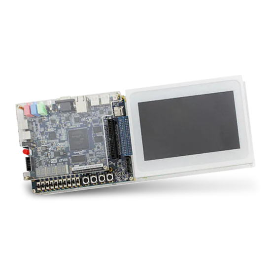
Summary of Contents for Terasic DE1-SoC-MTL2
-
Page 2: Table Of Contents
CHAPTER 3 ....................13 3.1 Using FPGA ............................. 13 3.2 Pin Definition of 2x20 GPIO Connector ....................13 3.3 Using LCD..............................15 3.4 Using Terasic Multi-touch IP ........................17 LINUX BSP CHAPTER 4 ........................20 4.1 Board Support Package ..........................20 4.2 Linux Image Files ............................. - Page 3 APPENDIX CHAPTER 6 ........................27 6.1 Revision History ............................27 6.2 Copyright Statement ..........................27 DE1-SoC-MTL2 User Manual www.terasic.com December 18, 2014...
-
Page 4: Chapter 1 Introduction
FPGA, as well as a 5-Point capacitive LCD multimedia color touch panel which natively supports five points multi-touch and gestures. The all-in-one embedded solution offered on the DE1-SoC-MTL2, in combination of a LCD touch panel and digital image module, provides embedded developers the ideal platform for multimedia applications with unparallel processing performance. -
Page 5: Key Features
I2C multiplexer Connectors o Two 40-pin expansion headers o One 10-pin ADC input header o One LTC connector (one Serial Peripheral Interface (SPI) master ,one I2C bus, and one GPIO interface) DE1-SoC-MTL2 User Manual www.terasic.com December 18, 2014... - Page 6 Sensor o G-sensor for the HPS Power o 12V DC input Capacitive LCD Touch Screen o Equipped with an 7-inch Amorphous-TFT-LCD (Thin Film Transistor Liquid Crystal Display) module o 800x600x3(RGB) Resolution DE1-SoC-MTL2 User Manual www.terasic.com December 18, 2014...
-
Page 7: About The Kit
Backlight power 1.674(Typ.) consumption Panel power 0.22(Typ.) consumption The kit includes everything users need to run the demonstrations and develop custom designs, as shown Figure 1-2. Figure 1-2 Contents of DE1-SoC-MTL2 kit package DE1-SoC-MTL2 User Manual www.terasic.com December 18, 2014... -
Page 8: Power On Test
Plug in the 12V DC power supply to the DE1-SoC board. Power on the DE1-SoC board. The LXDE Desktop will appear on the LCD display. Use the touch-screen to select the system menu, as shown in Figure 1-4. Figure 1-3 MSEL[4:0] = 00000 DE1-SoC-MTL2 User Manual www.terasic.com December 18, 2014... -
Page 9: System Cd And Linux Bsp
The DE1-SoC-MTL2 System CD contains the touch-screen documentations and supporting materials, including the user manual, reference designs, and device datasheets. Users can download the System CD form the link: http://cd-de1-soc-mtl2.terasic.com. This site also provides the Linux image files for creating a bootable microSD card. -
Page 10: Chapter 2 Architecture
Chapter 2 Architecture This chapter provides information regarding the features and architecture of DE1-SoC-MTL2. The kit is composed of DE1-SoC mainboard and MTL (Multi-Touch LCD) module. The MTL module is connected to a 2x20 GPIO expansion header on DE1-SoC board through an ITG (IDE to GPIO) adaptor. -
Page 11: Block Diagram
Figure 2-2 DE1-SoC-MTL2 (bottom view) Figure 2-3 shows the block diagram of MTL2 module. The IDE connector bridges all the wires from the peripherals to the FPGA through an ITG adapter. Figure 2-3 Block diagram of MTL2 DE1-SoC-MTL2 User Manual www.terasic.com... -
Page 12: Itg Adapter
Figure 2-4 illustrates the connection of MTL2 to Terasic FPGA board. Figure 2-4 Connection Diagram of MTL2 Kit with Terasic FPGA boards The IDE to GPIO (ITG) adapter is designed to remap IDE pins to GPIO pins. Figure 2-5 Figure 2-6 show the top and bottom view of ITG adapter, respectively. - Page 13 Figure 2-5 ITG adapter (top view) Figure 2-6 ITG adapter (bottom view) DE1-SoC-MTL2 User Manual www.terasic.com December 18, 2014...
-
Page 14: Using De1-Soc-Mtl2
The DE1-SoC SoC development board with the FPGA device is considered as the main part. The DE1-SoC user manual and CD are available at: http://cd-de1-soc.terasic.com The 2x20 GPIO female connector directly connects to the 2x20 GPIO male connector on the Terasic FPGA development boards. Figure 3-1 shows the signal names of the 2x20 GPIO from the ITG adapter. - Page 15 3.3-V LVTTL Output MTL_R[4] 3.3-V LVTTL Output MTL_R[5] 3.3-V LVTTL Output MTL_R[6] 3.3-V LVTTL Output MTL_R[7] 3.3-V LVTTL Output MTL_G[0] 3.3-V LVTTL Output MTL_G[1] 3.3-V LVTTL Output MTL_G[2] 3.3-V LVTTL Output MTL_G[3] 3.3-V LVTTL DE1-SoC-MTL2 User Manual www.terasic.com December 18, 2014...
-
Page 16: Using Lcd
Horizontal Display Area thd DCLK DCLK Frequency fclk 26.4 33.3 46.8 MHz One Horizontal Line 862 1056 1200 DCLK HS pulse width thpw 40 DCLK HS Blanking 46 DCLK HS Front Porch thfp 210 354 DCLK DE1-SoC-MTL2 User Manual www.terasic.com December 18, 2014... - Page 17 VS period time 510 525 650 TH VS pulse width tvpw 20 TH VS Blanking 23 TH HS Front Porch tvfp 147 TH Figure 3-2 Horizontal input timing waveform Figure 3-3 Vertical input timing waveform DE1-SoC-MTL2 User Manual www.terasic.com December 18, 2014...
-
Page 18: Using Terasic Multi-Touch Ip
Terasic Multi-touch IP is provided for developers to retrieve user inputs, including multi-touch gestures and single-touch. The file name of this IP is i2c_touch_config.v, which is located in System CD \IP folder. The IP decodes I2C information and outputs coordinates and gesture information. The inputs and... - Page 19 Figure 3-4 Signaltap II Waveform for Multi-Touch IP Table 3-4 Definition of Terasic Multi-touch IP Signals Pin Name Direction Description iCLK Input Connect to 50MHz clock iRSTN Input Connect to system reset signal INT_n Input Connect to interrupt pin of touch IC...
- Page 20 Zoom In 0x48 Zoom Out 0x49 No Gesture 0x00 Note: The Terasic IP Multi-touch IP can also be found under the \IP folder in the system CD, as well as the reference designs. DE1-SoC-MTL2 User Manual www.terasic.com December 18, 2014...
-
Page 21: Chapter 4 Linux Bsp
Chapter 4 Linux BSP This chapter describes how to use the Linux BSP (Board Support Package) provide by Terasic. Users can develop touch-screen GUI program easily with the BPS including QT 5.3.1 library. Figure 4-1 shows the block diagram of Linux BSP for DE1-SoC-MTL2 kit. The BPS incudes three major parts: ... -
Page 22: Linux Image Files
LXDE desktop Linux image file is provided for DE1-SoC-MTL2. It is available from the link: http://cd-de1-soc-mtl2.terasic.com. Developers can use a tool named Win32 Disk Imager to write the image file into a microSD card. For details about how to create a bootable microSD card or... -
Page 23: Qt Libraries
Users can develop touch-screen GUI program based on the QT library. For more information, please refer to the document “Software Development Guide for touch-screen display.pdf” included in the DE1-SoC-MTL2 system CD. The precompiled libraries can be found from the folder “Demonstrations/SoC_FPGA/Libraries” in the DE1-SoC-MTL2 system CD. -
Page 24: Chapter 5 Painter Demonstration
If a gesture is detected, the associated gesture symbol will be shown in the gesture area. To clear the painting area, click the “Clear” button. Figure 5-1 GUI of Painter Demo DE1-SoC-MTL2 User Manual www.terasic.com December 18, 2014... - Page 25 Figure 5-2 shows the single-finger painting of canvas area. Figure 5-2 Single-finger painting Figure 5-3 shows the zoom-in gesture. Figure 5-3 Zoom-in gesture Figure 5-4 5-Point painting of canvas area. Figure 5-4 5-Point painting DE1-SoC-MTL2 User Manual www.terasic.com December 18, 2014...
-
Page 26: System Description
IP must be installed before compiling the Quartus II project including this encrypted component. Figure 5-5 shows the system generic block diagram of painter demonstration. Figure 5-5 System block diagram of painter demonstration Please follow the procedures below to setup the demonstration: DE1-SoC-MTL2 User Manual www.terasic.com December 18, 2014... -
Page 27: Demonstration Source Code
1. Connect the DE1-SoC-MTL2 USB-Blaster II USB port to the PC USB Port with a USB Cable. 2. Power on the DE1-SoC-MTL2. 3. Please make sure Quartus II v14.0 has been installed on the host PC. 4. Copy the folder \Demonstrations\FPGA\DE1_SoC_MTL2_PAINTER\demo_batch. -
Page 28: Chapter 6 Appendix
Chapter 6 Appendix Version Change Log V1.0 Initial Version (Preliminary) Copyright © 2014 Terasic Technologies. All rights reserved. DE1-SoC-MTL2 User Manual www.terasic.com December 18, 2014...
Need help?
Do you have a question about the DE1-SoC-MTL2 and is the answer not in the manual?
Questions and answers