Table of Contents
Advertisement
Quick Links
Advertisement
Table of Contents

Related Manuals for Terasic TSOM


Summary of Contents for Terasic TSOM
-
Page 2: Table Of Contents
TABLE OF CONTENTS Chapter 1 Introduction ........................2 1.1 TSoM Design Package ........................2 1.2 Getting Help ............................2 Chapter 2 Board Specification ......................3 2.1 Layout and Components ........................3 2.2 Block Diagram ............................ 3 2.3 Mechanical Specifications ........................5 2.4 Power Requirement .......................... -
Page 3: Chapter 1 Introduction
(BSP) software to help you create a fully customized embedded design without starting from scratch. The TSoM design package contains all the documents and supporting materials associated with TSoM module, including the user manual, system builder, reference designs, and device datasheets. -
Page 4: Chapter 2 Board Specification
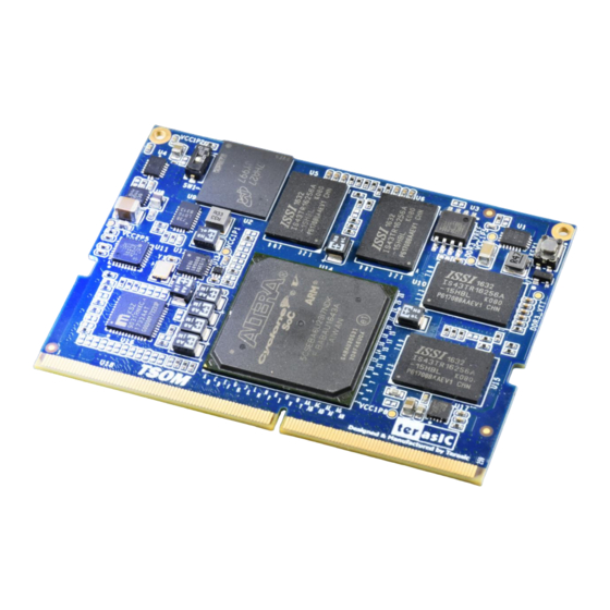
Figure 2-1 Mechanical Layout of the TSoM Module Figure 2-2 is the block diagram of the module. The most FPGA I/Os of TSoM module are all connected to the onboard 260-pin Edge connector, then it’s easy to connected to customer’s main board. - Page 5 Figure 2-2 Block diagram of the TSoM Module Detailed information about Figure 2-2 are listed below. ◼ Module: ⚫ FPGA: Cyclone V SE 5CSEBA6U23I7NDK (110K LEs) ⚫ Interface: DDR4 Edge (include 3.3V power source) ⚫ Dimension: 50 mm x 70 mm ◼...
-
Page 6: Mechanical Specifications
Size 70 x50mm The TSoM module is powered by the 260-pin edge connector. The user only needs to supply 3.3V/6A to the 260-pin edge connector of the TSoM module. The power circuit on the TSoM module can convert 3.3V to 1.1V/1.2V/1.5V/1.8V/2.5V, which then is supplied to the FPGA and other components. - Page 7 Figure 2-4 Power Tree of the TSoM Module www.terasic.com TSoM User Manual March 8, 2019...
-
Page 8: Chapter 3 System Interface
Chapter 3 System Interface This chapter will introduce the system level interfaces on the TSoM module. Users can get the Boot method of the HPS, the clock and reset system on the module, and the detailed pin distribution of the 260-pin edge connector connected externally. - Page 9 SD card socket or QSPI flash, the external SD card socket is used as the HPS boot source. Only one of the two boot sources can be chosen for the boot source on TSoM board . User can control the multiplexer and choose eMMC or external boot device as the boot source through SW1,...
- Page 10 Figure 3-4 HPS_BOTSEL[2..0] resistors setting ◼ EPCS There is an EPCS64 configuration device reserved on the TSoM module. The EPCS device is a flash memory device that can store configuration data that you use for FPGA configuration purpose after powering on. You can use the EPCS device on all FPGAs that support AS x1configuration scheme.
-
Page 11: Clock System
Figure 3-7 MSEL[4:0] Setting Resistors on the TSoM Module (Bottom Side) The clock source on the TSoM module is provided by an Si5350C clock generator, which can generate several groups of clocks for the devices on the TSoM module. The Si5350C generates 25MHz clock for the clock groups in the HPS, and provides two 50MHz clocks for the FPGA fabric to drive customer’s design. -
Page 12: Reset System
Figure 3-8 Clock System of the TSoM Module The TSoM module provides warm reset and cold reset function for the HPS, as shown in the Figure 3-9. The cold reset comes from external mainboard and is used for HPS Ethernet PHY, USB OTG PHY and eMMC memory through the 260-pin edge connector. - Page 13 JTAG function. Users can refer to TSoM schematic for the detailed signal connections. Users can connect the TSoM module to the main board that contains DDR4 SODIMM socket. Table 3-2 lists the several recommended DDR4 SODIMM sockets for reference.
-
Page 14: Hps Fabric Components
DDR3, Ethernet, eMMC and USB OTG. The TSoM module has a single Host/Device (USB OTG) USB 2.0 PHY that connects to the SoC device, the PHY can operate in USB host, USB device and USB On-The-Go (host and device capable) modes. -
Page 15: Gigabit Ethernet
Note: There is only a Giga Ethernet PHY on the TSoM module (without any ethernet physical interface, eg. J45), for using this function, users need to connect a TSoM Based Board (or other customized expansion board) to implement the connection between the Giga Ethernet PHY and a ethernet physical interface. -
Page 16: Emmc
TSoM module. Note: As described in the section 3.1, the eMMC on the TSoM module and the external SD Card interface (on the 260-pin Edge Connector) share the same HPS data bus. If user wants to select eMMC to boot HPS, please set the SW1 to "On"... -
Page 17: Hps 3.3V Gpio
Qsys built in Quartus software. 25 HPS I/Os of TSoM module are connected to the 260-pin edge connector, then users can connect the HPS peripherals to the main board according to their own design requirements, such as UART, I2C, CAN and HPS GPIO interface. - Page 18 PIN_C16 CAN0_TX UART0_TX SPIM1_SS0 HPS_GPIO66 HPS_V3P3_GPIO19 PIN_A8 QSPI_IO0 USB1_CLK HPS_GPIO29 HPS_V3P3_GPIO20 PIN_H16 QSPI_IO1 USB1_STP HPS_GPIO30 HPS_V3P3_GPIO21 PIN_A7 QSPI_IO2 USB1_DIR HPS_GPIO31 HPS_V3P3_GPIO22 PIN_J16 QSPI_IO3 USB1_NXT HPS_GPIO32 HPS_V3P3_GPIO23 PIN_A6 QSPI_SS0 HPS_GPIO33 HPS_V3P3_GPIO24 PIN_C14 QSPI_CLK HPS_GPIO34 www.terasic.com TSoM User Manual March 8, 2019...
-
Page 19: Ddr3
HPS DDR3 Bank Address[1] SSTL-15 Class I HPS_DDR3_BA2 PIN_G25 HPS DDR3 Bank Address[2] SSTL-15 Class I HPS_DDR3_CAS_N PIN_A26 DDR3 Column Address Strobe SSTL-15 Class I HPS_DDR3_CKE0 PIN_L28 HPS DDR3 Clock Enable SSTL-15 Class I www.terasic.com TSoM User Manual March 8, 2019... - Page 20 HPS DDR3 Data Strobe n[0] Differential 1.5-V SSTL Class I HPS_DDR3_DQS_N1 PIN_R18 HPS DDR3 Data Strobe n[1] Differential 1.5-V SSTL Class I HPS_DDR3_DQS_N2 PIN_T18 HPS DDR3 Data Strobe n[2] Differential 1.5-V SSTL Class I www.terasic.com TSoM User Manual March 8, 2019...
- Page 21 For output drive calibration SSTL-15 Class I HPS_DDR3_ODT1 PIN_G26 HPS DDR3 On-die Termination SSTL-15 Class I HPS_DDR3_CKE1 PIN_K28 HPS DDR3 Clock Enable SSTL-15 Class I HPS_DDR3_CS_N1 PIN_L20 HPS DDR3 Chip Select SSTL-15 Class I www.terasic.com TSoM User Manual March 8, 2019...
-
Page 22: Fpga Fabric Components
DDR3 Address[10] SSTL-15 Class I FPGA_DDR3_ADDR11 PIN_AF27 DDR3 Address[11] SSTL-15 Class I FPGA_DDR3_ADDR12 PIN_AA23 DDR3 Address[12] SSTL-15 Class I FPGA_DDR3_ADDR13 PIN_AF25 DDR3 Address[13] SSTL-15 Class I FPGA_DDR3_ADDR14 PIN_AE25 DDR3 Address[14] SSTL-15 Class I TSoM User Manual www.terasic.com March 8, 2019... - Page 23 SSTL-15 Class I FPGA_DDR3_DQ23 PIN_AE19 FPGA DDR3 Data[23] SSTL-15 Class I FPGA_DDR3_DQ24 PIN_AH21 FPGA DDR3 Data[24] SSTL-15 Class I FPGA_DDR3_DQ25 PIN_AH22 FPGA DDR3 Data[25] SSTL-15 Class I FPGA_DDR3_DQ26 PIN_AG23 FPGA DDR3 Data[26] SSTL-15 Class I www.terasic.com TSoM User Manual March 8, 2019...
-
Page 24: Fpga Ios On 260-Pin Edge Connector
5-2). It also comes with DC +3.3V (VCC3P3) and GND pins. Table 5-3 shows all the pin assignments of the FPGA GPIO pins on 260-pin edge connector. Figure 5-2 IO Connections between FPGA and 260-pin edge connector interface www.terasic.com TSoM User Manual March 8, 2019... - Page 25 LVDS RX or CMOS I/O LVDS_CLKIN_n3 PIN_108 PIN_W20 LVDS-RX or 2.5V or differential clock input LVDS RX or CMOS I/O LVDS_CLKIN_p0 PIN_258 PIN_V11 LVDS-RX or 2.5V or differential clock input www.terasic.com TSoM User Manual March 8, 2019...
- Page 26 PIN_199 PIN_AF8 LVDS-TX or 2.5V CMOS I/O LVDS TX bit n9 or LVDS_TX_n9 PIN_193 PIN_AF4 LVDS-TX or 2.5V CMOS I/O LVDS TX bit n10 or LVDS_TX_n10 PIN_187 PIN_AH2 LVDS-TX or 2.5V CMOS I/O www.terasic.com TSoM User Manual March 8, 2019...
- Page 27 PIN_224 PIN_V10 LVDS-RX or 2.5V CMOS I/O LVDS RX bit n6 or LVDS_RX_n6 PIN_218 PIN_T8 LVDS-RX or 2.5V CMOS I/O LVDS RX bit n7 or LVDS_RX_n7 PIN_212 PIN_Y8 LVDS-RX or 2.5V CMOS I/O www.terasic.com TSoM User Manual March 8, 2019...
- Page 28 LVDS-RX or 2.5V CMOS I/O LVDS RX bit p9 or LVDS_RX_p9 PIN_192 PIN_T13 LVDS-RX or 2.5V CMOS I/O LVDS RX bit p10 or LVDS-RX or 1.8V or 2.5V LVDS_RX_p10 PIN_186 PIN_D12 CMOS I/O or 3.3V www.terasic.com TSoM User Manual March 8, 2019...
- Page 29 Appendix Table A-1 Terasic TSoM Module Pinout FPGA Pin Pin Num Pin Name Description Direction Standard Power supply 12V (no use) Power Power supply 12V (no use) Power Power supply 12V (no use) Power Power supply 12V (no use) Power 3.3V...
- Page 30 Power Power supply GND Power Power supply GND Power Power supply GND Power Power supply GND Power Power supply GND Power Power supply GND Power Power supply GND Power Power supply GND Power www.terasic.com TSoM User Manual March 8, 2019...
- Page 31 Input / HPS_ V3P3_GPIO9 details, please refer to the HPS 3.3V PIN_A18 Output MUX table. HPS General-purpose IO, for Input / HPS_ V3P3_GPIO10 details, please refer to the HPS 3.3V PIN_C17 Output MUX table. www.terasic.com TSoM User Manual March 8, 2019...
- Page 32 3.3V PIN_A6 Output MUX table. HPS General-purpose IO, for Input / HPS_ V3P3_GPIO24 details, please refer to the HPS 3.3V PIN_C14 Output MUX table. HPS_nPOR HPS Cold reset, Active low, Output 3.3V PIN_H19 www.terasic.com TSoM User Manual March 8, 2019...
- Page 33 SD Card data line 3 3.3V Output DIM_SD_DATA4 No use DIM_SD_DATA5 No use DIM_SD_DATA6 No use DIM_SD_DATA7 No use USB Current-Limit Switch Enable USB_CPEN output 3.3V signal. USB_DM USB Data Minus, Connection to Input / 3.3V www.terasic.com TSoM User Manual March 8, 2019...
- Page 34 LVDS or LVDS_RX_p1 LVDS RX or Single-Ended I/O PIN_AE12 Output 1.8V/2.5V Input/ LVDS or LVDS_RX_n2 LVDS RX or Single-Ended I/O PIN_AF10 Output 1.8V/2.5V LVDS_RX_p2 LVDS RX or Single-Ended I/O Input/ LVDS or PIN_AF11 www.terasic.com TSoM User Manual March 8, 2019...
- Page 35 LVDS or LVDS_CLKIN_n3 PIN_W20 Input or Single-Ended I/O Output 1.8V/2.5V LVDS RX / Differential Clock Input/ LVDS or LVDS_CLKIN_p3 PIN_W21 Input or Single-Ended I/O Output 1.8V/ 2.5V RX_n12 No Connection RX_p12 No Connection www.terasic.com TSoM User Manual March 8, 2019...
- Page 36 LVDS_TX_p5 LVDS TX or Single-Ended I/O PIN_AC4 Output 1.8V/2.5V Input/ LVDS or LVDS_TX_n6 LVDS TX or Single-Ended I/O PIN_Y4 Output 1.8V/2.5V Input/ LVDS or LVDS_TX_p6 LVDS TX or Single-Ended I/O PIN_Y5 Output 1.8V/2.5V www.terasic.com TSoM User Manual March 8, 2019...
- Page 37 TX_p17 No Connection TX_n18 No Connection TX_p18 No Connection TX_n19 No Connection TX_p19 No Connection TX_n21 No Connection TX_p21 No Connection TX_n22 No Connection TX_p22 No Connection TX_n23 No Connection TX_p23 No Connection www.terasic.com TSoM User Manual March 8, 2019...
- Page 38 No Connection V2P5_GPIO4 No Connection V2P5_GPIO5 No Connection V3P3_GPIO0 No Connection V3P3_GPIO1 No Connection V3P3_GPIO2 No Connection V3P3_GPIO3 No Connection Version Change Log V1.0 Initial Version (Preliminary) Copyright © Terasic Inc. All rights reserved. www.terasic.com TSoM User Manual March 8, 2019...
Need help?
Do you have a question about the TSOM and is the answer not in the manual?
Questions and answers