Table of Contents
Advertisement
Quick Links
Advertisement
Table of Contents

Related Manuals for Terasic ALTERA ICB HSMC


Summary of Contents for Terasic ALTERA ICB HSMC
-
Page 2: Table Of Contents
CONTENTS Chapter 1 Introduction ..................3 1.1 Features ................................3 1.2 About the Kit ..............................4 1.3 Getting Help ..............................5 Chapter 2 ICB Architecture ................. 6 2.1 Layout and Components..........................6 2.2 Block Diagram of the ICB..........................7 Chapter 3 Board Components................9 3.1 HSMC Expansion Connector ........................9 3.2 GPIO Interface ............................12 3.3 RS-232 Interface ............................13 3.4 RS-485 Interface ............................14... - Page 3 6.1 Revision History............................32 6.2 Copyright Statement...........................32 ...
-
Page 4: Chapter 1 Introduction
Chapter 1 Introduction The Industrial Communication Board (ICB-HSMC) is designed to provide common industry standard interfaces for FPGA platforms that support RS-232, RS-485, and CAN connectivity through a High-Speed Mezzanine Connector (HSMC). It allows users to setup a communication network for industrial use through the industrial standard interfaces on the ICB. This board features one RS-232 interface, one GPIO interface, four RS-485 interfaces, two CAN interfaces, and four PIO interfaces. -
Page 5: About The Kit
• HSMC Connector • 40-Pin GPIO interface o 36 user I/Os • Two 6-Pin PIO interfaces o 4 user I/Os per interface • 12-Pin PIO interface o 8 user I/Os • RS-232 interface o Maxim RS-232 transceiver (MAX3238) support streaming transmission up to 250kbps o Complete RS-232 signal interface o 1 male DB9 Connector and one 10-pin header (shares pins with DB9 Connector) •... -
Page 6: Getting Help
Figure 1-2 ICB contents Getting Help Getting Help Here is information of how to get help if you encounter any problems: • Terasic Technologies • Tel: +886-3-550-8800 • Email: support@terasic.com... -
Page 7: Chapter 2 Icb Architecture
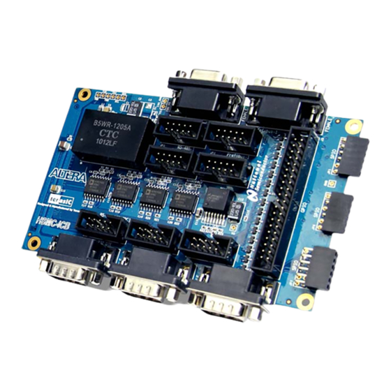
Chapter 2 ICB Architecture This chapter describes the architecture of the ICB including block diagram and components. Layout and Components Layout and Components The picture of the ICB is shown in Figure 2-1 Figure 2-2. It depicts the layout of the board and indicates the locations of the connectors and key components. -
Page 8: Block Diagram Of The Icb
Figure 2-2 The ICB-HSMC PCB and component diagram (bottom view) The following interfaces are provided on the ICB: • HSMC Connector (J7) • 40-pin GPIO Header (J3) • 6-pin Header (JP1/JP6) • 12-pin Header(JP7) • 10-pin Header (JP2/JP3/JP4/JP5/JP6/JP9/JP10) • DB9 Connector (J1/J2/J4/J5/J6) Block Diagram of the ICB Block Diagram of the ICB Figure 2-3... - Page 9 Figure 2-3 Block diagram of ICB-HSMC...
-
Page 10: Board Components
Chapter 3 Board Components This chapter describes the components, connectors, and pin assignments on the ICB. HSMC Expansion Connector HSMC Expansion Connector The HSMC interface provides a mechanism to extend the peripheral set of an FPGA host board by means of a mezzanine card, which can address today’s high speed signaling requirement as well as standard or legacy low-speed device interface support. - Page 11 GPIO_DATA6 Input/Output GPIO data GPIO_DATA2 Input/Output GPIO data GPIO_DATA7 Input/Output GPIO data GPIO_DATA3 Input/Output GPIO data VCC3P3 Power Power 3.3V VCC12 Power Power 12V GPIO_DATA12 Input/Output GPIO data GPIO_DATA8 Input/Output GPIO data GPIO_DATA13 Input/Output GPIO data GPIO_DATA9 Input/Output GPIO data VCC3P3 Power Power 3.3V...
- Page 12 PIO1_DATA0 Input/Output PIO1 data PIO0_DATA0 Input/Output PIO0 data PIO1_DATA1 Input/Output PIO1 data PIO0_DATA1 Input/Output PIO0 data VCC3P3 Power Power 3.3V VCC12 Power Power 12V PIO1_DATA2 Input/Output PIO1 data PIO0_DATA2 Input/Output PIO0 data PIO1_DATA3 Input/Output PIO1 data PIO0_DATA3 Input/Output PIO0 data VCC3P3 Power Power 3.3V...
-
Page 13: Gpio Interface
VCC12 Power Power 12V CAN1_T Output CAN channel 1 TXD CAN0_T Output CAN channel 0 TXD CAN1_R Input CAN channel 1 RXD CAN0_R Input CAN channel 0 RXD VCC3P3 Power Power 3.3V VCC12 Power Power 12V RS232_RXD Input RS-232 RXD VCC3P3 Power Power 3.3V... -
Page 14: Rs-232 Interface
GPIO is widely used for housing various application needs such as video processing or image acquisition, etc. It supports up to 50MHz data rate using a reliable cable connection. Each data pin on the GPIO is connected to an extra protection circuit made up of two clamping diodes and one serial resistor. -
Page 15: Rs-485 Interface
Figure 3-3 Wiring between the HSMC and RS-232 interface The male RS-232 connector provides the industrial standard cabling interface, in addition to a 10-pin header used for simple communication conditions where a specific cable is not needed. RS-485 Interface RS-485 Interface This section describes RS-485 interface on the ICB-HSMC. - Page 16 Figure 3-4 Wiring between HSMC and RS-485 interface Table 3-2 gives the pin assignments on 10-pin headers and DB9 connectors for RS-485 signals. Table 3-2 Pin assignments and descriptions for RS-485 interfaces RS-485 Channel Signal Name 10-pin Header DB9 connector RS485_0_A 5(JP3) 3(J2)
-
Page 17: Can Interface
CAN Interface CAN Interface This section describes the CAN interface on the ICB-HSMC. The board features two CAN links from the HSMC connector to two DB9 male connectors and two 10-pin headers. These two 10-pin headers share the same pins with two DB9 connectors. Figure 3-5 shows the connections between the HSMC and the CAN interface through a CAN transceiver chip. - Page 18 Figure 3-6 Wiring between HSMC and PIO interface...
-
Page 19: Assembling The Icb
Chapter 4 Assembling the ICB This chapter gives instructions for connecting the ICB to versatile host boards. Assemble ICB with DE2-115 Assemble ICB with DE2-115 For connecting the ICB to the DE2-115 board, plug the ICB to the HSMC ‘socket’ (JP8) of the DE2-115 board. -
Page 20: Generate Icb Project Via De2-115 System Builder
Figure 4-2 HSMC VCCIO supply voltage setting header (JP7) Generate ICB Project via DE2-115 System Builder Generate ICB Project via DE2-115 System Builder The DE2-115 board comes with a useful utility that helps users generate top level design and pin assignment files that include specific HSMC daughter card information. - Page 21 Figure 4-3 The DE2-115 System Builder window Input Project Name Input project name as show in Figure 4-4. Project Name: Type in an appropriate name here, it will automatically be assigned as the name of your top-level design entity.
- Page 22 Figure 4-4 The DE2-115 Board Type and Project Name System Configuration Under System Configuration, users can enable the desired components on the FPGA host board as shown in Figure 4-5. If the component is enabled, the DE2-115 System Builder will automatically generate the associated pin assignments, including the pin names, pin locations, pin directions, and I/O standards.
- Page 23 Figure 4-5 System Configuration Group HSMC Expansion Figure 4-6 illustrates the usage of the DE2-115 System Builder specifying ICB connecting to the HSMC interface. This will automatically generate wiring connections between the host board and ICB-HSMC.
- Page 24 Figure 4-6 HSMC Expansion Group The “Prefix Name” is an optional feature that denotes the pin name of the daughter card assigned in your design. Users may leave this field empty. Figure 4-7 illustrates the generated top level design file contains information on the ICB-HSMC connections.
- Page 25 Figure 4-7 Top level design file includes ICB-HSMC information...
-
Page 26: Chapter 5 Icb Demonstrations
Chapter 5 ICB Demonstrations This chapter mainly depicts how to use the ICB through a set of demonstrations located on the software CD. From running the demonstrations, users will know how to implement codes on the DE2-115 for controlling the ICB-HSMC. The demos include communication between RS-232 and PC, RS-485 loopback test, and CAN loopback test. - Page 27 Figure 5-1 Block diagram of RS-232 communication Demonstration source code • Project Directory: \Demonstrations\DE2_115_ICB_RS232 • Bit Stream Used: DE2_115_ICB_RS232.sof PC terminal software • Software Directory: \Demonstrations\DE2_115_ICB_RS232\SW • Executable File : UartTerminal.exe Demonstration batch file • Batch File Folder: \Demonstrations\DE2_115_ICB_RS232\demo_batch • Batch File: DE2_115_ICB_RS232.bat, test_bashrc •...
-
Page 28: Rs-485 Loopback Test
Figure 5-2 Terminal software interface RS-485 Loopback Test RS-485 Loopback Test This demonstration illustrates a loopback test through RS-485 interfaces using the UART protocol. Channel 0 of the RS-485 interface (marked as Profibus-1) connects to RS-485 channel 1. Software running on Nios II will first set channel 0 on transmit state and channel 1 on receive state, then it initiates one data transfer with its content set by SW7-0 through channel 0. - Page 29 Demonstration source code • Project Directory: \Demonstrations\ DE2_115_ICB_RS485 • Bit Stream Used: DE2_115_ICB_RS485.sof • NIOS II Workspace: \Demonstrations\ DE2_115_ICB_RS485\software Demonstration batch file • Batch File Folder: \Demonstrations\DE2_115_ICB_RS485\demo_batch • Batch File: DE2_115_ICB_RS485.bat, test_bashrc • FPGA Configuration File: DE2_115_ICB_RS485.sof Demonstration setup: • Connect ICB to DE2-115.
-
Page 30: Can Loopback Test
Figure 5-5 Test results on the prompt window Table 5-1 Loopback test result on HEXs for RS-485 Test Pass Info. Test failed info. S-<test data*> FAIL *test data represents the value set by SW15-8 or SW7-0. CAN Loopback Test CAN Loopback Test This demonstration illustrates how to construct a communication loop between two CAN interfaces where one initiates the data transfer and the other receives data then sends it back to the loop. - Page 31 Figure 5-6 Block diagram of CAN loopback test Demonstration source code • Project Directory: \Demonstrations\ DE2_115_ICB_CAN • Bit Stream Used: DE2_115_ICB_CAN.sof • NIOS II Workspace: \Demonstrations\ DE2_115_ICB_CAN\software Demonstration batch file • Batch File Folder: \Demonstrations\DE2_115_ICB_ CAN\ demo_batch • Batch File: DE2_115_ICB_ CAN.bat, test_bashrc •...
- Page 32 Figure 5-7 Wiring for CAN loopback test Figure 5-8 Prompt information while running the test Table 5-2 Loopback test result on HEXs for CAN Test Pass Info. Test failed info. S-<test data*> FAIL *test data represents the value set by SW7-0.
-
Page 33: Chapter 6 Appendix
Chapter 6 Appendix Revision History Revision History Version Change Log V1.0 Initial Version (Preliminary) Copyright Statement Copyright Statement Copyright © 2010 Terasic Technologies. All rights reserved.
Need help?
Do you have a question about the ALTERA ICB HSMC and is the answer not in the manual?
Questions and answers