Table of Contents
Advertisement
Advertisement
Table of Contents

Related Manuals for Terasic DE0-CV


Summary of Contents for Terasic DE0-CV
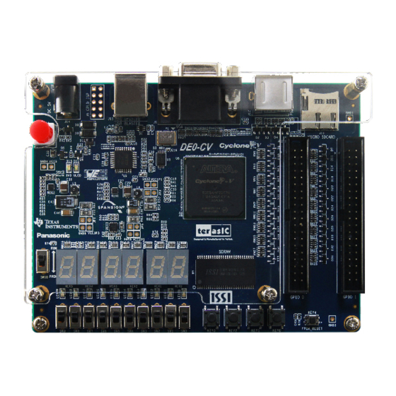
- Page 1 DE0-CV User Manual www.terasic.com May 4, 2015...
-
Page 2: Table Of Contents
2. 5 SD Card ............................14 2. 6 VGA .............................. 15 2. 7 Overall Structure of the DE0-CV Control Panel ................16 Chapter 3 Using the Starter Kit ..................18 3. 1 Configuration of Cyclone V FPGA on DE0-CV ................18 3. - Page 3 Chapter 5 Examples of Advanced Demonstrations ........... 43 5. 1 DE0-CV Factory Configuration ....................43 5. 2 SDRAM Test in Nios II ......................... 45 5. 3 SDRAM Test in Verilog ........................ 48 5. 4 PS/2 Mouse Demonstration......................49 5. 5 Micro SD Card file system read ....................
-
Page 4: Chapter 1 Introduction
By leveraging all of these capabilities, the DE0-CV is the perfect solution for showcasing, evaluating, and prototyping the true potential of the Altera Cyclone V FPGA. The DE0-CV contains all components needed to use the board in conjunction with a computer that runs the Microsoft Windows XP or later. -
Page 5: De0-Cv System Cd
The DE0-CV System CD contains the documentation and supporting materials, including the User Manual, Control Panel, System Builder, reference designs and device datasheets. User can download this System CD from the web (http://cd-de0-cv.terasic.com). This section presents the features and design characteristics of the board. - Page 6 3080 Kbits embedded memory 4 Fractional PLLs Serial Configuration device – EPCS64 on FPGA On-Board USB Blaster (Normal type B USB connector) JTAG and AS mode configuration supported DE0-CV User Manual www.terasic.com May 4, 2015...
-
Page 7: Block Diagram Of The Cyclone V Starter Board
To provide maximum flexibility for the user, all connections are made through the Cyclone V FPGA device. Thus, the user can configure the FPGA to implement any system design. DE0-CV User Manual www.terasic.com May 4, 2015... -
Page 8: Getting Help
Here are the addresses where you can get help if you encounter any problem: Terasic Inc. 9F., No.176, Sec.2, Gongdao 5th Rd, East Dist, Hsinchu City, 30070. Taiwan Email: support@terasic.com Tel.: +886-3-5750-880 Web: http://www.DE0-CV.terasic.com DE0-CV User Manual www.terasic.com May 4, 2015... -
Page 9: Chapter 2 Control Panel
Chapter 2 Control Panel The DE0-CV board comes with a Control Panel program that allows users to access various components on the board from a host computer. The host computer communicates with the board through a USB connection. The program can be used to verify the functionality of components on the board or be used as a debug tool while developing any RTL code. - Page 10 LEDs and observing the result on the DE0-CV board. Figure 2-1 The DE0-CV Control Panel The “Control Circuit” that The concept of the DE0-CV Control Panel is illustrated in Figure 2-2. performs the control functions is implemented in the FPGA board. It communicates with the Control Panel window, which is active on the host computer, via the USB Blaster link.
-
Page 11: Controlling The Leds, 7-Segment Displays
Figure 2-2 The DE0-CV Control Panel concept The DE0-CV Control Panel can be used to light up LEDs, change the values displayed on the 7-segment, monitor buttons/switches status, read/write the SDRAM Memory, output VGA color pattern to VGA monitor, read SD Card specification information. The feature of reading/writing a word or an entire file from/to the Memory allows the user to develop multimedia applications without worrying about how to build a Memory Programmer. - Page 12 Figure 2-4. From the window, directly use the left-right arrows to control the 7-SEG patterns on the DE0-CV board which are updated immediately. Note that the dots of the 7-SEGs are not enabled on the DE0-CV board. Figure 2-4 Controlling 7-SEG display DE0-CV User Manual www.terasic.com...
-
Page 13: Switches And Push-Buttons
Thus, it can be used for troubleshooting purposes. The Control Panel can be used to write/read data to/from the SDRAM chips on the DE0-CV board. As shown below, we will describe how the SDRAM may be accessed; Click on the Memory tab and select “SDRAM”... - Page 14 The Control Panel also supports loading files with a .hex extension. Files with a .hex extension are ASCII text files that specify memory values using ASCII characters to represent hexadecimal values. For example, a file containing the line 0123456789ABCDEF DE0-CV User Manual www.terasic.com May 4, 2015...
-
Page 15: Sd Card
1. Choosing the SD Card tab leads to the window in Figure 2-7. 2. Insert an SD Card to the DE0-CV board, and then press the Read button to read the SD Card. The SD Card‟s identification, specification, and file format information will be displayed in the control window. -
Page 16: Vga
Choosing the VGA tab leads to the window in Figure 2-8. Plug a D-sub cable to the VGA connector of the DE0-CV board and LCD /CRT monitor. The LCD/CRT monitor will display the same color pattern on the control panel window. -
Page 17: Overall Structure Of The De0-Cv Control Panel
Figure 2-8 Controlling VGA display under Control Panel The DE0-CV Control Panel is based on a Nios II Qsys system instantiated in the Cyclone V FPGA with software running on the on-chip memory. The software part is implemented in C code; the hardware part is implemented in Verilog HDL code with Qsys builder. - Page 18 Figure 2-9 The block diagram of the DE0-CV control panel DE0-CV User Manual www.terasic.com May 4, 2015...
-
Page 19: Using The Starter Kit
DE0-CV board is turned off. When the board‟s power is turned on, the configuration data in the EPCS64 device is automatically loaded into the Cyclone V FPGA. - Page 20 Figure 3-2) Connect the USB cable provided to the USB Blaster port on the DE0-CV board The FPGA can now be programmed by using the Quartus II Programmer to select a configuration bit stream file with the .sof filename extension...
- Page 21 Ensure that power is applied to the DE0-CV board. Connect the USB cable provided to the USB Blaster port on the DE0-CV board Configure the JTAG programming circuit by setting the RUN/PROG slide switch (SW10) to the PROG position.
-
Page 22: Using The Leds And Switches
Cyclone V device as shown in Figure 3-5. Each of these switches is debounced using a Schmitt Trigger circuit, as indicated in Figure 3-6. The five outputs called KEY0, KEY1, DE0-CV User Manual www.terasic.com May 4, 2015... - Page 23 Cyclone V FPGA. When the switch is in the DOWN position (closest to the edge of the board), it provides a low logic level to the FPGA, and when the switch is in the UP position it provides a high logic level. DE0-CV User Manual www.terasic.com May 4, 2015...
- Page 24 LED on, and driving the pin low turns it off. Figure 3-8 shows the connections between LEDs and Cyclone V FPGA. Table 3-2, Table 3-3 Table 3-4 list the pin assignment of user push-buttons, switches, and LEDs. DE0-CV User Manual www.terasic.com May 4, 2015...
- Page 25 FPGA Pin No. Description PIN_U13 Slide Switch[0] PIN_V13 Slide Switch[1] PIN_T13 Slide Switch[2] PIN_T12 Slide Switch[3] PIN_AA15 Slide Switch[4] PIN_AB15 Slide Switch[5] PIN_AA14 Slide Switch[6] PIN_AA13 Slide Switch[7] PIN_AB13 Slide Switch[8] PIN_AB12 Slide Switch[9] DE0-CV User Manual www.terasic.com May 4, 2015...
-
Page 26: Using The 7-Segment Displays
LED [8] LEDR9 PIN_L1 LED [9] The DE0-CV board has six 7-segment displays. These displays are paired to display numbers in various sizes. Figure 3-9 shows the connection of seven segments (common anode) to pins on Cyclone V FPGA. The segment can be turned on or off by applying a low logic level or high logic level from the FPGA, respectively. - Page 27 Seven Segment Digit 5[1] HEX52 PIN_T14 Seven Segment Digit 5[2] HEX53 PIN_P14 Seven Segment Digit 5[3] HEX54 PIN_C1 Seven Segment Digit 5[4] HEX55 PIN_C2 Seven Segment Digit 5[5] HEX56 PIN_W19 Seven Segment Digit 5[6] DE0-CV User Manual www.terasic.com May 4, 2015...
-
Page 28: Clock Circuitry
Figure 3-10 shows the clock circuit of DE0-CV Board, the crystal 50 MHz buffered to four 50MHz clock. The associated pin assignment for clock inputs to FPGA I/O pins is listed in Table 3-6. Figure 3-10 Clock circuit of the FPGA Board... - Page 29 GPIO Connection 0[0] GPIO_0_D1 PIN_B16 GPIO Connection 0[1] GPIO_0_D2 PIN_M16 GPIO Connection 0[2] GPIO_0_D3 PIN_C16 GPIO Connection 0[3] GPIO_0_D4 PIN_D17 GPIO Connection 0[4] GPIO_0_D5 PIN_K20 GPIO Connection 0[5] GPIO_0_D6 PIN_K21 GPIO Connection 0[6] DE0-CV User Manual www.terasic.com May 4, 2015...
- Page 30 GPIO Connection 1[11] GPIO_1_D12 PIN_J19 GPIO Connection 1[12] GPIO_1_D13 PIN_G11 GPIO Connection 1[13] GPIO_1_D14 PIN_H10 GPIO Connection 1[14] GPIO_1_D15 PIN_J11 GPIO Connection 1[15] GPIO_1_D16 PIN_H14 GPIO Connection 1[16] GPIO_1_D17 PIN_A15 GPIO Connection 1[17] DE0-CV User Manual www.terasic.com May 4, 2015...
-
Page 31: Using Vga
PIN_K16 GPIO Connection 1[35] The DE0-CV board includes a 16-pin D-SUB connector for VGA output. The VGA synchronization signals are provided directly from the Cyclone V FPGA, and a 4-bit DAC using resistor network is used to produce the analog data signals (red, green, and blue). The associated schematic is given in Figure 3-13 and can support standard VGA resolution (640x480 pixels, at 25 MHz). - Page 32 Pixel clock(MHz) clock clock clock clock cycle) cycle) cycle) cycle) VGA(60Hz) 640x480 Table 3-9 VGA Vertical Timing Specification VGA mode Vertical Timing Spec Configuration Resolution(HxV) a(lines) b(lines) c(lines) d(lines) Pixel clock(MHz) VGA(60Hz) 640x480 DE0-CV User Manual www.terasic.com May 4, 2015...
-
Page 33: Ps/2 Serial Port
VGA H_SYNC VGA_VS PIN_G8 VGA V_SYNC The DE0-CV board comes with a standard PS/2 interface and a connector for a PS/2 keyboard or mouse. Figure 3-15 shows the connection of PS/2 circuit to the FPGA. Users can use the PS/2... -
Page 34: Micro Sd-Card Socket
SD Card and Cyclone V FPGA and Figure 3-18 shows micro SD card plug-in position. Finally, Table 3-12 lists all the associated pins. Figure 3-17 Connection between the SD Card Socket and Cyclone V FPGA DE0-CV User Manual www.terasic.com May 4, 2015... -
Page 35: Using Sdram
16-bit data line, control line, and address line connected to the FPGA. This chip uses the 3.3V LVCMOS signaling standard. Connections between the FPGA and SDRAM are shown in Figure 3-19, and the pin assignment is listed in Table 3-13. DE0-CV User Manual www.terasic.com May 4, 2015... - Page 36 SDRAM Data[1] DRAM_DQ2 PIN_R9 SDRAM Data[2] DRAM_DQ3 PIN_Y11 SDRAM Data[3] DRAM_DQ4 PIN_R10 SDRAM Data[4] DRAM_DQ5 PIN_R11 SDRAM Data[5] DRAM_DQ6 PIN_R12 SDRAM Data[6] DRAM_DQ7 PIN_AA12 SDRAM Data[7] DRAM_DQ8 PIN_AA9 SDRAM Data[8] DRAM_DQ9 PIN_AB8 SDRAM Data[9] DE0-CV User Manual www.terasic.com May 4, 2015...
- Page 37 SDRAM byte Data Mask[1] PIN_AB6 DRAM_RAS_N SDRAM Row Address Strobe PIN_V6 DRAM_CAS_N SDRAM Column Address Strobe PIN_R6 DRAM_CKE SDRAM Clock Enable PIN_AB11 DRAM_CLK SDRAM Clock PIN_AB5 DRAM_WE_N SDRAM Write Enable PIN_U6 DRAM_CS_N SDRAM Chip Select DE0-CV User Manual www.terasic.com May 4, 2015...
-
Page 38: De0-Cv System Builder
Figure 4-1. The DE0-CV System Builder will generate two major files, a top-level design file (.v) and a Quartus II setting file (.qsf) after users launch the DE0-CV System Builder and create a new project according to their design requirements DE0-CV User Manual www.terasic.com... -
Page 39: Using De0-Cv System Builder
4. 3 Using DE0-CV System Builder This section provides the procedures in details on how to use the DE0-CV System Builder. Install and Launch the DE0-CV System Builder The DE0-CV System Builder is located in the directory: “Tools\SystemBuilder” of the DE0-CV System CD. - Page 40 Figure 4-2 The GUI of DE0-CV System Builder Enter Project Name Enter the project name in the circled area, as shown in Figure 4-3. The project name typed in will be assigned automatically as the name of your top-level design entity.
- Page 41 4-4. Each component onboard is listed and users can enable or disable one or more components at will. If a component is enabled, the DE0-CV System Builder will automatically generate its associated pin assignment, including the pin name, pin location, pin direction, and I/O standard.
- Page 42 The “Prefix Name” is an optional feature that denote the pin name of the daughter card assigned in your design. Users may leave this field blank. Project Setting Management The DE0-CV System Builder also provides the option to load a setting or save users‟ current board configuration in .cfg file, as shown in Figure 4-6.
- Page 43 DE0-CV System Builder will generate the corresponding Quartus II files and documents, as listed in Table 4-1: Figure 4-7 Generate Quartus Project Table 4-1 Files generated by the DE0-CV System Builder Filename Description <Project name>.v Top level Verilog HDL file for Quartus II <Project name>.qpf...
-
Page 44: Examples Of Advanced Demonstrations
Copy the folder Demonstrations to a local directory of your choice. It is important to make sure the path to your local directory contains NO space. Otherwise it will lead to error in Nios II. Note : Quartus II v14.0 or later is required for all DE0-CV demonstrations to support Cyclone V FPGA device. - Page 45 Power on the DE0-CV board with the USB cable connected to the USB-Blaster port. If necessary (that is, if the default factory configuration is not currently stored in the EPCS device), download the bit stream to the board via JTAG interface.
-
Page 46: Sdram Test In Nios Ii
The SDRAM controller is configured as a 64MB controller. The working frequency of the SDRAM controller is 143 MHz, and the Nios II program is running on the on-chip memory. DE0-CV User Manual www.terasic.com May 4, 2015... - Page 47 Nios II Eclipse v14.0 Quartus project directory: DE0_CV_SDRAM_Nios_Test Nios II Eclipse directory: DE0_CV_SDRAM_Nios_Test \Software Click “Clean” from the “Project” menu of Nios II Eclipse before compiling the reference design in Nios II Eclipse. DE0-CV User Manual www.terasic.com May 4, 2015...
- Page 48 Press any button (KEY3~KEY0) to start the SDRAM verification process. Press KEY0 to run the test continuously. The program will display the test progress and result, as shown in Figure 5-3. Figure 5-3 Display of progress and result for the SDRAM test in Nios II DE0-CV User Manual www.terasic.com May 4, 2015...
-
Page 49: Sdram Test In Verilog
KEY0 triggers test control signals for the SDRAM, and the LEDs will indicate the test result according to Table 5-1. Quartus II v14.0 Project directory: DE0_CV_SDRAM_RTL_Test Bitstream used: DE0_CV_SDRAM_RTL_Test.sof DE0-CV User Manual www.terasic.com May 4, 2015... -
Page 50: Ps/2 Mouse Demonstration
More information about the PS/2 protocol can be found on various websites. DE0-CV User Manual www.terasic.com May 4, 2015... - Page 51 After the power on cycle of the PS/2 mouse, it enters into stream mode automatically and disable data transmit unless an enabling instruction is received. Figure 5-5 shows the waveform while communication happening on two lines. DE0-CV User Manual www.terasic.com May 4, 2015...
- Page 52 Figure 5-5 Waveform of clock and data signals during data transmission Project directory: DE0_CV_PS2_DEMO Bitstream used: DE0_CV_PS2_DEMO.sof Demo batch file directoy: \DE0_CV_PS2_DEMO \demo_batch The folder includes the following files: Batch file: DE0_CV_PS2_DEMO.bat FPGA configuration file : DE0_CV_PS2_DEMO.sof DE0-CV User Manual www.terasic.com May 4, 2015...
- Page 53 The 7-segment display should change when the PS/2 mouse moves. The LEDR[2:0] will blink according to Figure 5-6 Table 5-2 when the left-button, right-button, and/or middle-button is pressed. Figure 5-6 Description of 7-segment Display and LED Indicators DE0-CV User Manual www.terasic.com May 4, 2015...
-
Page 54: Micro Sd Card File System Read
Many applications use a large external storage device, such as a SD Card or CF card to store data. The DE0-CV board provides the hardware and software needed for Micro SD Card access. In this demonstration we will show how to browse files stored in the root directory of an SD Card and how to read the file contents of a specific file. - Page 55 LEDR9~LEDR5 if it fails to parse the FAT file system or if there is no SD card found in the SD Card socket of the DE0-CV board. If users press KEY3 of the DE0-CV board, the program will perform the above process again.
- Page 56 After Nios II program is downloaded and executed successfully, a prompt message will be displayed in nios2-terminal. Copy DE0_CV_SD_DEMO\demo_batch\test.txt files to the root directory of the SD Card. Insert the Micro SD Card into the SD Card socket of DE0-CV, as shown in Figure 5-9. DE0-CV User Manual www.terasic.com...
- Page 57 Figure 5-9 Insert the Micro SD card into DE0-CV Press KEY3 of the DE0-CV board to start reading SD Card. The program will display SD Card information, as shown in Figure 5-10. Figure 5-10 Running result of SD_CARD demo on DE0-CV board DE0-CV User Manual www.terasic.com...
-
Page 58: Vga Pattern
Figure 5-11 Block diagram of the VGA Pattern demonstration Figure 5-12 Timing Waveform of VGA interface Quartus II 14.1 Quartus Project directory: DE0_CV_VGA_Pattern Bitstream used: DE0_CV_VGA_Pattern.sof Demo Batch File Folder: DE0_CV_SD_DEMO\demo_batch\ The demo batch file includes following files: DE0-CV User Manual www.terasic.com May 4, 2015... - Page 59 Quartus II v14.1 must be pre-installed to the host PC.. Power on the DE0-CV board. Connect USB Blaster to the DE0-CV board and install USB Blaster driver if necessary. Connect VGA D-SUB to a VGA monitor.
- Page 60 9F., No.176, Sec.2, Gongdao 5th Rd, East Dist, Hsinchu City, 30070. Taiwan Email: support@terasic.com Web: www.terasic.com DE0-CV Web: www.DE0-CV.terasic.com Date Version Changes 2014.12 First publication 2015.04 Document revision 2015.5 Modified DE0-CV package content figure DE0-CV User Manual www.terasic.com May 4, 2015...
- Page 61 Mouser Electronics Authorized Distributor Click to View Pricing, Inventory, Delivery & Lifecycle Information: Terasic P0192...
Need help?
Do you have a question about the DE0-CV and is the answer not in the manual?
Questions and answers