Table of Contents
Advertisement
Quick Links
Advertisement
Table of Contents

Related Manuals for Terasic HAN Pilot Platform


Summary of Contents for Terasic HAN Pilot Platform
-
Page 2: Table Of Contents
TABLE OF CONTENTS Chapter 1 Overview ........................3 1.1 The Package Contents ..........................4 1.2 HAN Pilot Platform System CD ......................... 4 1.3 Getting Help ............................... 4 Chapter 2 Board Components ......................6 2.1 Components and Layout ..........................6 2.2 Block Diagram ............................9 Chapter 3 Board Settings and Status Component ................ - Page 3 Power .......................... 69 Chapter 8 HAN Pilot Platform System Builder ................70 8.1 Introduction .............................. 70 8.2 General Design Flow ..........................70 8.3 Using HAN Pilot Platform System Builder ....................71 Chapter 9 Appendix ........................79 HAN Pilot Platform www.terasic.com...
-
Page 4: Chapter 1 Overview
The hardware offers in the HAN Pilot Platform has the maximum capacity with 660K LEs in Arria 10 SoC FPGA and featuring various types of high-speed image interface such as: HDMI, Display Port, and 12G-SDI and a large capacity of DDR4 memory. -
Page 5: The Package Contents
7. One 4GB DDR4 ECC SO-DIMM Module (Installed) 8. Screws, Copper Stands, and Silicon Footstands The HAN Pilot Platform System CD contains all the documents and supporting materials associated with HAN Pilot Platform, including the user manual, system builder, reference designs and device datasheets. -
Page 6: July
▪ Tel.: +886-3-575-0880 ▪ Website: HAN Pilot Platform.terasic.com HAN Pilot Platform www.terasic.com Hardware Manual July 5, 2019... -
Page 7: Chapter 2 Board Components
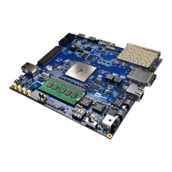
Figure 2-1 Figure 2-2 shows a photograph of the board. It depicts the layout of the board and indicates the location of the connectors and key components. Figure 2-1 HAN Pilot Platform (top view) HAN Pilot Platform www.terasic.com Hardware Manual... - Page 8 Figure 2-2 HAN Pilot Platform (bottom view) The HAN Pilot Platform has many features that allow users to implement a wide range of designed circuits, from simple circuits to various multimedia projects. The following hardware are provided on the board: ◼...
- Page 9 • USB OTG Port, USB mini-AB connector • UART to USB, USB Mini-B connector • • One user button and one user LED • Warm reset button and cold reset button HAN Pilot Platform www.terasic.com Hardware Manual July 5, 2019...
-
Page 10: 2.2 Block Diagram
Buttons x3 (FPGA x2, HPS x1) ▪ Switches x2 on FPGA ▪ LEDs x3 (FPGA x2, HPS x1) ▪ 7-segment displays x2 ▪ System Monitor and Control ▪ Temperature Sensor on FPGA ▪ 12V Power Monitor HAN Pilot Platform www.terasic.com Hardware Manual July 5, 2019... - Page 11 ▪ Power Controller ▪ I2C Fan Control ▪ Power ▪ 12V DC input Figure 2-3 Block diagram of HAN Pilot Platform HAN Pilot Platform www.terasic.com Hardware Manual July 5, 2019...
-
Page 12: Board Settings And Status Component
◼ Mode Select Switches Mode Select Switch (SW5) is used to set the HAN Pilot Platform FPGA MSEL pin value. These MSEL pins determined the Configuration Mode of the FPGA. -
Page 13: Board Setting Headers
Pilot Platform system. The FMC connector will not be included in the JTAG chain if the headers are set to open (See Figure 3-3). Table 3-2 list the setting of the J17 header. HAN Pilot Platform www.terasic.com Hardware Manual July 5, 2019... - Page 14 JP2 is used to set the VCCIO voltage of FPGA I/O on FMC connector, as 1.2V/1.5V/1.8V are supported, the FMC connector can support various I/0 standard FMC daughtercards. Table 3-3 list the FMC_VCCIO Headers Setting. Table 3-3 FMC_VCCIO Headers Setting JP2 Setting FMC VCCIO Voltage 1.2V HAN Pilot Platform www.terasic.com Hardware Manual July 5, 2019...
- Page 15 Figure 3-4 The FMC VCCIO select header ◼ PMODE Select Header The USB 3.0 Controller (Cypress FX3) on the HAN Pilot Platform can be booted from the different sources, selected by the configuration of the PMODE header (JP4/JP5/JP6) on HAN Pilot Platform.
-
Page 16: Status Led
Figure 3-5 The PMODE select header This section describes the all status LED for the interfaces on HAN Pilot Platform board. Figure shows all the status LED on the HAN Pilot Platform. Following are the detailed descriptions of these interface LED. HAN Pilot Platform www.terasic.com... -
Page 17: Uart Interface
Figure 3-6 The status LED on the HAN Pilot Platform board ◼ UART Interface Table 3-5 list the two status LEDs for UART interface. Table 3-5 Status LED for UART Interface Component Reference Status Descriptions TXD1 UART_TXD Transmitting RXD1 UART_RXD Receiving ◼... -
Page 18: Jtag Interface
Pilot Platform JTAG Chain, or exclude them from the JTAG Chain. The default JTAG path for HAN Pilot Platform is: USB Blaster II ==> HPS ==> FPGA ==> (Bypass FMC connector) ==> USB Blaster II. When the External JTAG connector is connected to the external blaster, the On board's USB blaster II function will be replaced by the external blaster. - Page 19 Figure 3-7 JTAG interface of HAN Pilot Platform HAN Pilot Platform www.terasic.com Hardware Manual July 5, 2019...
-
Page 20: Fpga Fabric Components
FPGA. When the switch is set to the UP position, a high logic level is generated to the FPGA. Table 4-2 list the pin assignment of switches. HAN Pilot Platform www.terasic.com Hardware Manual July 5, 2019... - Page 21 Arria 10 SoC FPGA. The segment can be turned on or off by applying a low logic level or high logic level from the FPGA, respectively. Each segment in a display is indexed from 0 to 6, HAN Pilot Platform www.terasic.com...
-
Page 22: Usb Type-C Port
1.8V HEX1_DP PIN_AR31 Seven Segment Digit 1_DP 1.8V The HAN Pilot Platform board features one USB Type-C connector. It is designed for high-speed data transmission with computers and image output applications. Figure 4-5 shows the block diagram of the connection between USB Type-C port and FPGA. -
Page 23: Display Port
4-6, USB Type-C port can connect to FPGA transceiver. Users can implement a Display port source mode IP in the FPGA, the HAN Pilot Platform board will implement the features of display port source. Through the USB Type-C cable, users can connect HAN Pilot Platform board to the monitor which supports Display port interface. - Page 24 Pin in Conjunction with 1.8 V Dx_SEL Pin Display port Switch USBDP_SW_CNF0 AA27 1.8 V Configure 0 Display port Switch USBDP_SW_CNF1 AB26 1.8 V Configure 1 USBDP_SW_CNF2 AB25 Display port Switch 1.8 V HAN Pilot Platform www.terasic.com Hardware Manual July 5, 2019...
- Page 25 Configure 2 ◼ USB 3.0 Device The HAN Pilot Platform board has one Cypress FX3 USB Controller (CYUSB3014). The USB controller is connected to FPGA through the programmable GPIF II interface, and connect to the external USB Type-C connector, it provides USB 3.0 Device application for HAN Pilot Platform board.
- Page 26 GPIF II Data Bus 30 1.8 V USBFX3_DQ[31] AP20 GPIF II Data Bus 31 1.8 V USBFX3_CTL0_SLCS_n AV26 GPIF II Control Bus 0 1.8 V USBFX3_CTL1_SLWR_n AT22 GPIF II Control Bus 1 1.8 V HAN Pilot Platform www.terasic.com Hardware Manual July 5, 2019...
-
Page 27: Sfp+ Connector
10 SoC FPGA device and transform them to optical signals. The board includes cage assemblies for the SFP+ connectors. Figure 4-9 shows the connections between the SFP+ and Arria 10 SoC FPGA. HAN Pilot Platform www.terasic.com Hardware Manual July 5, 2019... - Page 28 Table 4-8 SFP+ B Pin Assignments, Signal Names and Functions FPGA Signal Name Description I/O Standard Number Turns off and disables the SFPB_TXDISABLE PIN_AU5 1.2V transmitter output SFPB_TXFAULT PIN_AE10 Transmitter fault 1.2V HAN Pilot Platform www.terasic.com Hardware Manual July 5, 2019...
- Page 29 Table 4-10 SFP+ D Pin Assignments, Signal Names and Functions FPGA Signal Name Description I/O Standard Number Turns off and disables the SFPD_TXDISABLE PIN_AR28 1.2V transmitter output SFPD_TXFAULT PIN_AP21 Transmitter fault 1.2V HSSI DIFFERENTIAL SFPD_TX_p PIN_AD39 Transmiter data HAN Pilot Platform www.terasic.com Hardware Manual July 5, 2019...
-
Page 30: Sata
SATA solution with a design that consists of both host and target (device side) functions. Figure 4-10 depicts the host and device design examples. Figure 4-10 PC and storage device connection to the Arria 10 SoC FPGA HAN Pilot Platform www.terasic.com Hardware Manual July 5, 2019... - Page 31 Differential transmit data HSSI SATA_DEVICE_TX_n0 PIN_B38 output before DIFFERENTIAL blocking capacitor Differential transmit data HSSI SATA_DEVICE_TX_n1 PIN_A36 output before DIFFERENTIAL blocking capacitor Differential transmit data HSSI SATA_DEVICE_TX_p0 PIN_B39 output before DIFFERENTIAL HAN Pilot Platform www.terasic.com Hardware Manual July 5, 2019...
- Page 32 SATA_HOST_TX_n1 PIN_AH38 output before DIFFERENTIAL blocking capacitor Differential receive data HSSI SATA_HOST_RX_n0 PIN_AE32 input after DC blocking DIFFERENTIAL capacitor Differential receive data HSSI SATA_HOST_RX_n1 PIN_AF34 input after DC blocking DIFFERENTIAL capacitor HAN Pilot Platform www.terasic.com Hardware Manual July 5, 2019...
-
Page 33: Pcie
Figure 4-14, the longest length is up to 3 meters. These two associated devices are not included in HAN Pilot Platform kit. To purchase the PCA card as well as the external cable, please refer to Terasic website pca.terasic.com and PCIe_Cable.terasic.com. - Page 34 Figure 4-13 PCIe External Cable Figure 4-14 PCIe Link Setup between HAN Pilot Platform and PC Table 4-12 summarizes the PCI Express pin assignments of the signal names relative to the Arria 10 FPGA. Table 4-12 PCI Express pin assignments of the signal names...
-
Page 35: Ddr4
SSTL-12 PIN_AN11 DDR4B_A[3] Address [3] SSTL-12 PIN_AM10 DDR4B_A[4] Address [4] SSTL-12 PIN_AM11 DDR4B_A[5] Address [5] SSTL-12 PIN_AP9 DDR4B_A[6] Address [6] SSTL-12 PIN_AN9 DDR4B_A[7] Address [7] SSTL-12 PIN_AR10 DDR4B_A[8] Address [8] SSTL-12 HAN Pilot Platform www.terasic.com Hardware Manual July 5, 2019... - Page 36 PIN_AP6 DDR4B_DQS_n[2] Data Strobe n[2] 1.2-V POD DIFFERENTIAL PIN_AT3 DDR4B_DQS_n[3] Data Strobe n[3] 1.2-V POD PIN_AF10 DDR4B_DBI_n[0] Data Bus Inversion [0] 1.2-V POD PIN_AL8 DDR4B_DBI_n[1] Data Bus Inversion [1] 1.2-V POD HAN Pilot Platform www.terasic.com Hardware Manual July 5, 2019...
- Page 37 1.2-V POD PIN_AR3 DDR4B_DQ[25] Data [25] 1.2-V POD PIN_AN3 DDR4B_DQ[26] Data [26] 1.2-V POD PIN_AR1 DDR4B_DQ[27] Data [27] 1.2-V POD PIN_AU2 DDR4B_DQ[28] Data [28] 1.2-V POD PIN_AP4 DDR4B_DQ[29] Data [29] 1.2-V POD HAN Pilot Platform www.terasic.com Hardware Manual July 5, 2019...
- Page 38 DDR4 SDRAM SODIMM and Arria 10 SoC FPGA. The pin assignments for DDR4 SDRAM SO-DIMM are listed in Table 4-14. Figure 4-16 The connection between the DDR4 SDRAM SO-DIMM and Arria 10 SoC FPGA HAN Pilot Platform www.terasic.com Hardware Manual July 5, 2019...
- Page 39 Clock n0 1.2-V SSTL PIN_AC2 DDR4A_CKE Clock Enable pin SSTL-12 DIFFERENTIAL PIN_AE8 DDR4A_DQS[0] Data Strobe p[0] 1.2-V POD DIFFERENTIAL PIN_AF7 DDR4A_DQS[1] Data Strobe p[1] 1.2-V POD PIN_AN1 DDR4A_DQS[2] Data Strobe p[2] DIFFERENTIAL HAN Pilot Platform www.terasic.com Hardware Manual July 5, 2019...
- Page 40 1.2-V POD PIN_AD10 DDR4A_DQ[1] Data [1] 1.2-V POD PIN_AC9 DDR4A_DQ[2] Data [2] 1.2-V POD PIN_AG7 DDR4A_DQ[3] Data [3] 1.2-V POD PIN_AD13 DDR4A_DQ[4] Data [4] 1.2-V POD PIN_AD11 DDR4A_DQ[5] Data [5] 1.2-V POD HAN Pilot Platform www.terasic.com Hardware Manual July 5, 2019...
- Page 41 1.2-V POD PIN_N2 DDR4A_DQ[34] Data [34] 1.2-V POD PIN_K2 DDR4A_DQ[35] Data [35] 1.2-V POD PIN_M2 DDR4A_DQ[36] Data [36] 1.2-V POD PIN_P3 DDR4A_DQ[37] Data [37] 1.2-V POD PIN_N1 DDR4A_DQ[38] Data [38] 1.2-V POD HAN Pilot Platform www.terasic.com Hardware Manual July 5, 2019...
- Page 42 1.2-V POD PIN_W1 DDR4A_DQ[67] Data [67] 1.2-V POD PIN_Y3 DDR4A_DQ[68] Data [68] 1.2-V POD PIN_W4 DDR4A_DQ[69] Data [69] 1.2-V POD PIN_U1 DDR4A_DQ[70] Data [70] 1.2-V POD PIN_U2 DDR4A_DQ[71] Data [71] 1.2-V POD HAN Pilot Platform www.terasic.com Hardware Manual July 5, 2019...
- Page 43 PIN_AA8 DDR4A_RZQ 1.2 V output drive calibration The DDR4 SDRAM SO-DIMM socket can support many kinds of memory devices, such as standard DDR4 SO-DIMM with ECC up to 8GB at 1067MHz, Terasic QDRII+ module, as shown Figure 4-17, Figure 4-18.
-
Page 44: Hdmi Transmitter And Receiver
Figure 4-17 Standard DDR4 SO-DIMM with ECC Figure 4-18 Terasic QDRII+ module with DDR4 SO-DIMM interface The HAN Pilot Platform board features HDMI transmitter and receiver. For HDMI transmitter, as shown in Figure 4-19. The board features a Transition Minimized Differential Signal (TMDS) retimer IC (TI:SN75DP159). - Page 45 Figure 4-19 The HDMI transceiver interface of the HAN Pilot Platform Table 4-15 HDMI TX and RX port Pin Assignments, Signal Names and Functions FPGA Pin Signal Name Description I/O Standard Number HDMI reference clock from HDMI_REFCLK_p LVDS external PLL...
-
Page 46: Gigabit Ethernet
Table 4-16 Ethernet PHY Pin Assignments, Signal Names and Functions Signal Name FPGA Pin Number Description I/O Standard ETH_TX_p PIN_AP19 SGMII TX data LVDS ETH_RX_p PIN_AM20 SGMII RX data LVDS ETH_INT_n PIN_AU19 Management bus interrupt 1.8V HAN Pilot Platform www.terasic.com Hardware Manual July 5, 2019... -
Page 47: Fmc Connector
JTAG, clock outputs and inputs, high-speed serial I/O (transceivers), and single-ended or differential signaling. There is one FMC connector on the HAN Pilot Platform board, it is a High Pin Count (HPC) size of connector, The HPC connector on HAN Pilot Platform board can provides 172 user-define, single-ended signals (include clock signals) and 10 serial transceiver pairs. - Page 48 FMC data bus 1.8 V FMC_HA_n[2] PIN_E10 FMC data bus 1.8 V FMC_HA_n[3] PIN_F12 FMC data bus 1.8 V FMC_HA_n[4] PIN_J13 FMC data bus 1.8 V FMC_HA_n[5] PIN_K11 FMC data bus 1.8 V HAN Pilot Platform www.terasic.com Hardware Manual July 5, 2019...
- Page 49 FMC data bus 1.8 V FMC_HB_p[11] PIN_AJ16 FMC data bus 1.8 V FMC_HB_p[12] PIN_AW13 FMC data bus 1.8 V FMC_HB_p[13] PIN_AV14 FMC data bus 1.8 V FMC_HB_p[14] PIN_AP14 FMC data bus 1.8 V HAN Pilot Platform www.terasic.com Hardware Manual July 5, 2019...
- Page 50 FMC data bus 1.8 V FMC_LA_p[0] PIN_A3 FMC data bus 1.8 V FMC_LA_p[1] PIN_B4 FMC data bus 1.8 V FMC_LA_p[2] PIN_T9 FMC data bus 1.8 V FMC_LA_p[3] PIN_M10 FMC data bus 1.8 V HAN Pilot Platform www.terasic.com Hardware Manual July 5, 2019...
- Page 51 FMC data bus 1.8 V FMC_LA_p[33] PIN_N11 FMC data bus 1.8 V FMC_LA_n[0] PIN_A4 FMC data bus 1.8 V FMC_LA_n[1] PIN_C3 FMC data bus 1.8 V FMC_LA_n[2] PIN_T10 FMC data bus 1.8 V HAN Pilot Platform www.terasic.com Hardware Manual July 5, 2019...
- Page 52 1.8 V FMC_LA_n[31] PIN_R10 FMC data bus 1.8 V FMC_LA_n[32] PIN_N6 FMC data bus 1.8 V FMC_LA_n[33] PIN_P11 FMC data bus 1.8 V LVDS input from FMC_GBTCLK_M2C_p[0] PIN_P31 LVDS installed card HAN Pilot Platform www.terasic.com Hardware Manual July 5, 2019...
- Page 53 DIFFERENTIAL HSSI FMC_DP_C2M_p[6] PIN_F39 Transmit channel DIFFERENTIAL HSSI FMC_DP_C2M_p[7] PIN_E37 Transmit channel DIFFERENTIAL HSSI FMC_DP_C2M_p[8] PIN_D39 Transmit channel DIFFERENTIAL HSSI FMC_DP_C2M_p[9] PIN_C37 Transmit channel DIFFERENTIAL HSSI FMC_DP_M2C_p[0] PIN_P35 Transmit channel DIFFERENTIAL HAN Pilot Platform www.terasic.com Hardware Manual July 5, 2019...
- Page 54 DIFFERENTIAL FMC geographical address FMC_GA[0] PIN_E11 1.8 V FMC geographical address FMC_GA[1] PIN_AL18 1.8 V Management serial clock FMC_SCL PIN_J9 1.8 V line FMC_SDA PIN_F4 Management serial data line 1.8 V HAN Pilot Platform www.terasic.com Hardware Manual July 5, 2019...
-
Page 55: Temperature Sensor, Fan Control And Power Monitor
FPGA. The board is equipped with a Fan-Speed regulator and monitor MAX6650 with an I2C/SMBus interfaces, Users regulate and monitor the speed of fan depending on the measured system temperature. The HAN Pilot Platform has implemented a power monitor chip to monitor the board input power voltage and current. Figure 4-22 shows the connection between the power monitor chip and the Arria 10 SoC FPGA. -
Page 56: Gyroscope, Accelerometer And Magnetometer
Active-low ALERT input 1.8V The HAN Pilot Platform board is equipped with a Motion-Tracking device named MPU-9250. The MPU-9250 is a 9-axis Motion-Tracking device that combines a 3-axis gyroscope, 3-axis accelerometer and 3-axis magnetometer. Detail features of these sensors are listed below. - Page 57 Communication with all registers of the device is performed using either I2C at 400kHz on the HAN Pilot platform. or SPI at 1MHz. For applications requiring faster communications, the sensor and interrupt registers may be read using SPI at 20MHz. The I2C address is 7’b1101001. For more detailed information of better using this chip, please refer to its datasheet which is available on manufacturer’s website or under the /datasheet folder of the system CD.
-
Page 58: Hps Fabric Components
5-2. More information about the KSZ9031RNX PHY chip and its datasheet, as well as the application notes, is available on the manufacturer’s website. Figure 5-1 Connections between the HPS and Gigabit Ethernet HAN Pilot Platform www.terasic.com Hardware Manual July 5, 2019... - Page 59 1000 Link / Activity (RX, TX) 100 Link / No Activity Toggle OFF Blinking 100 Link / Activity (RX, TX) 10 Link/ No Activity Toggle Toggle Blinking Blinking 10 Link / Activity (RX, TX) HAN Pilot Platform www.terasic.com Hardware Manual July 5, 2019...
-
Page 60: Uart To Usb
An USB to Serial device (Cypress: CY7C65215) is used on the HAN Pilot Platform to connect to other on-board devices through JTAG / UART / I2C interface. Let Host PC can communicate with these devices through the USB interface (See Figure 5-2). -
Page 61: Micro Sd Card Socket
USB type-A port. Figure 5-4 shows the connections of USB PTG PHY to the HPS. Table 5-6 lists the pin assignment of USB OTG PHY to the HPS. HAN Pilot Platform www.terasic.com Hardware Manual July 5, 2019... -
Page 62: Gpio Header
Stop Data Stream on the Bus 1.8V There is a 2x5 pin header(2.54mm) on the HAN Pilot Platform which connected to six FPGA HPS fabric GPIOs. These I/Os can be used as GPIO that are directly controlled by HPS. Or it can be used as SPI interface (HPS_DIO[11:8]), using the SPI master controller in HPS to communicate with other SPI devices. -
Page 63: Ddr4 (Hps)
DDR4 devices by FPGA fabric. Figure 3 26 shows the connections between the DDR4 and Arria 10 SoC FPGA. Table 3 18 lists the pin assignment of DDR4 and its description with I/O standard. HAN Pilot Platform www.terasic.com Hardware Manual... - Page 64 Address [15]/CAS_n SSTL-12 PIN_L28 DDR4H_A[16] Address [16]/RAS_n SSTL-12 PIN_AU6 DDR4H_BA[0] Bank Select [0] SSTL-12 PIN_AP8 DDR4H_BA[1] Bank Select [1] SSTL-12 PIN_AN8 DDR4H_BG[0] Bank Group Select[0] SSTL-12 PIN_AJ14 DDR4H_BG[1] Bank Group Select[1] SSTL-12 HAN Pilot Platform www.terasic.com Hardware Manual July 5, 2019...
- Page 65 1.2-V POD PIN_AF12 DDR4H_DQ[5] Data [5] 1.2-V POD PIN_AJ10 DDR4H_DQ[6] Data [6] 1.2-V POD PIN_AG10 DDR4H_DQ[7] Data [7] 1.2-V POD PIN_AL9 DDR4H_DQ[8] Data [8] 1.2-V POD PIN_AH9 DDR4H_DQ[9] Data [9] 1.2-V POD HAN Pilot Platform www.terasic.com Hardware Manual July 5, 2019...
- Page 66 DDR4H_RESET_n Chip Reset 1.2 V PIN_Y28 DDR4H_ODT On Die Termination SSTL-12 Command and Address Parity PIN_T27 DDR4H_PAR SSTL-12 Input PIN_A23 DDR4H_ALERT_n Register ALERT_n output SSTL-12 PIN_Y25 DDR4H_ACT_n Activation Command Input SSTL-12 HAN Pilot Platform www.terasic.com Hardware Manual July 5, 2019...
- Page 67 External reference ball for PIN_J26 DDR4H_RZQ 1.2 V output drive calibration HAN Pilot Platform www.terasic.com Hardware Manual July 5, 2019...
-
Page 68: Chapter 6 System Clocks
System Clocks Figure 6-1 shows the Clock Net connected to FPGA on HAN Pilot Platform. The Si5350c provides the fixed system frequencies to FPGA, HPS and other important components. There are four 50 MHz connected to the dedicated clock pins of the FPGA, which can be used by PLL for clock multiplier or frequency division. - Page 69 Figure 6-2 The default settings for different PLLs HAN Pilot Platform www.terasic.com Hardware Manual July 5, 2019...
-
Page 70: Chapter 7 Power
Power Figure 7-1 is HAN Pilot Platform Power Tree. HAN Pilot Platform can be supplied by the 12V power adapter in the package, or external connecting to USB Type-C as power supply. The maximum load of the system supports is 60W (FPGA usage is 92 %) by our test. -
Page 71: Han Pilot Platform System Builder
▪ Pin Assignment Document (.htm) The above files generated by the HAN Pilot Platform System Builder can also prevent occurrence of situations that are prone to compilation error when users manually edit the top-level design file or place pin assignment. The common mistakes users may encounter are: ▪... -
Page 72: Using Han Pilot Platform System Builder
The HAN Pilot Platform System Builder is located in the directory: “Tools\SystemBuilder” of the HAN Pilot Platform System CD. Users can copy the entire folder to a host computer without installing the utility. A window will pop up, as shown in... - Page 73 Figure 8-2 The GUI of HAN Pilot Platform System Builder ◼ Enter Project Name Enter the project name in the circled area, as shown in Figure 8-3. The project name typed in will be assigned automatically as the name of your top-level design entity.
- Page 74 The system builder can generate Verilog or VHDL Quartus top file according to users’ requirement. Users can select their desired file type in the Top File Type list-box shown in Figure 8-4. HAN Pilot Platform www.terasic.com Hardware Manual July 5, 2019...
-
Page 75: System Configuration
I/O standards. Note: The pin assignments for some components (e.g. DDR4 and SFP+) require associated controller codes in the Quartus project or it would result in compilation error. Hence please do not select them if they are not needed in the design. HAN Pilot Platform www.terasic.com Hardware Manual... - Page 76 Figure 8-5 System Configuration group ◼ FMC Expansion If users connect any compatible Terasic FMC-based daughter cards to the FMC connector on HAN Pilot Platform, the HAN Pilot Platform System Builder can generate a project that include the corresponding module, as shown in Figure 8-6.
- Page 77 Verilog which facilitates users’ implementation as no additional control code is required to configure the programmable oscillator. Note: If users need to dynamically change the frequency, they would need to modify the generated control code themselves. HAN Pilot Platform www.terasic.com Hardware Manual July 5, 2019...
- Page 78 The System Builder also provides functions to restore default setting, load a setting, and save board configuration file, as shown in Figure 8-8. Users can save the current board configuration information into a .cfg file and load it into the System Builder. HAN Pilot Platform www.terasic.com Hardware Manual July 5, 2019...
- Page 79 Figure 8-8 Project Settings ◼ Project Generation When users press the Generate button, the HAN Pilot Platform System Builder will generate the corresponding Quartus Prime files and documents as listed in Table 8-1. Table 8-1 The files generated by HAN Pilot Platform System Builder...
-
Page 80: Chapter 9 Appendix
Date Change Log V1.0 10/24, 2018 Initial Version (Preliminary) V1.1 7/5, 2019 Modify FPP x32 mode MSEL setting to 000 ◼ Copyright Statement Copyright © 2018 Terasic Inc. All rights reserved. HAN Pilot Platform www.terasic.com Hardware Manual July 5, 2019...
Need help?
Do you have a question about the HAN Pilot Platform and is the answer not in the manual?
Questions and answers