Table of Contents
Advertisement
Quick Links
Advertisement
Table of Contents

Related Manuals for Terasic ALTERA DE4


Summary of Contents for Terasic ALTERA DE4
- Page 1 DE4 User Manual www.terasic.com June 20, 2018...
- Page 2 CONTROL PANEL CHAPTER 3 ..........................74 3.1 C ............................74 ONTROL ANEL ETUP 3.2 C .................... 78 ONTROLLING THE S AND EGMENT ISPLAYS 3.3 SWITCH/BUTTON ............................... 80 3.4 M ............................81 EMORY ONTROLLER DE4 User Manual www.terasic.com June 20, 2018...
-
Page 3: Table Of Contents
5.7 P ............................142 OWER EASUREMENT 5.8 W ................................. 146 ERVER 5.9 S ATA (SATA) ............................. 155 ERIAL 5.10 H (HSMC) ......................156 PEED EZZANINE 5.11 PCI ............................158 EMONSTRATION ADDITIONAL INFORMATION ........................... 159 DE4 User Manual www.terasic.com June 20, 2018... - Page 4 ASIC prototype development, it can be established by a cable connecting to multiple DE4/FPGA boards through the HSMC connectors. It is highly recommended that users read the DE4 .pdf before using the DE4 Getting Started Guide DE4 User Manual www.terasic.com June 20, 2018...
- Page 5 I2C EEPROM General user input/output: o 8 LEDs o 4 push-buttons and 4 slide switches o 8-position DIP switch o 2 seven-segment displays Clock system o On-board clock oscillators: 50MHz and 100MHz DE4 User Manual www.terasic.com June 20, 2018...
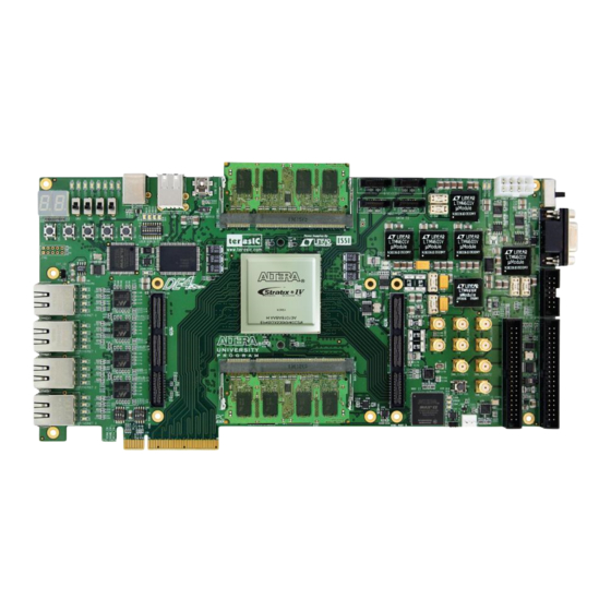
- Page 6 Users can refer to this figure for relative location when the connectors and key components are introduced in the following chapters. Figure 1–1 The DE4 board (Top view) DE4 User Manual www.terasic.com June 20, 2018...
- Page 7 DE4 board. To provide maximum flexibility for the users, all key components are connected with the Stratix IV GX FPGA device. Thus, users can configure the FPGA to implement any system design. DE4 User Manual www.terasic.com June 20, 2018...
- Page 8 Figure 1–3 Block diagram of the DE4 board Below is more detailed information regarding the blocks in Figure 1–3. DE4 User Manual www.terasic.com June 20, 2018...
- Page 9 Programmable PLL timing chip configured via MAX II CPLD Support JTAG mode Memory devices 64MB Flash (32M x16) with a 16-bit data bus 2MB SSRAM (1M x 16) 2Kb EEPROM DE4 User Manual www.terasic.com June 20, 2018...
- Page 10 When a switch is set to the DOWN or UP position, it causes logic 0 or 1, respectively. On-Board Clocking Circuitry 50MHz/100MHz oscillator 2 SMA connector for external transceiver clock input 4 SMA connector for LVDS clock input/output 2 SMA connectors for clock output DE4 User Manual www.terasic.com June 20, 2018...
- Page 11 72 FPGA I/O pins, as well as 4 power and ground lines, are brought out to two 40-pin expansion connectors 40-pin header is designed to accept a standard 40-pin ribbon cable used for IDE hard drives Compatible with I/O standard 3.3V DE4 User Manual www.terasic.com June 20, 2018...
- Page 12 Support data transfer at high-speed, full-speed, and low-speed Support both USB host and device Three USB ports (one type mini-AB for host/device and two type A for host) Support Nios II with the Terasic driver Power Standalone DC inputs 12V and 3.3V ...
- Page 13 USB-to-JTAG configuration logic using a type-B USB connector, a FTDI USB 2.0 Controller, and an Altera MAX II CPLD. Current configuration will be lost when the power is turned off. Figure 2–1 illustrates the JTAG configuration scheme for the DE4. DE4 User Manual www.terasic.com June 20, 2018...
- Page 14 The DE4 development board contains a common flash interface (CFI) flash memory to meet the demands for a larger FPGA configuration storage. The parallel flash loader (PFL) feature in MAX II devices provides an efficient method to program CFI flash memory devices through the JTAG DE4 User Manual www.terasic.com June 20, 2018...
- Page 15 DE4. Software Requirements: Quartus II 9.1 SP2 or later Nios II IDE tools 9.1 SP2 or later Program_flash folder contents: Program_flash.bat Program_flash.pl Program_flash.sh DE4 User Manual www.terasic.com June 20, 2018...
- Page 16 1. Launch the program_flash.bat batch file from the directory (\demonstrations\de4_<Stratix device>\de4_board_update_portal\demo_batch\Program_flash) of the DE4 system CD-ROM. 2. The flash program tool shows the menu options. Figure 2–3 Flash program tools 3. Select option 2. DE4 User Manual www.terasic.com June 20, 2018...
- Page 17 ‘Extracting FPGA Image SREC’, and ‘Deleting intermediate files’. If these lines don’t appear on the windows command, programming on the flash memory is not successfully setup. Please make sure Quartus II 9.1 SP2 and Nios II 9.1 IDE SP2 or later is used. DE4 User Manual www.terasic.com June 20, 2018...
- Page 18 Figure 2–6 Loading .sof file to be program 6. Erasing flash. Figure 2–7 Erasing flash Programming flash. DE4 User Manual www.terasic.com June 20, 2018...
- Page 19 Figure 2–8 Programming flash Programming complete. Figure 2–9 Programming flash complete DE4 User Manual www.terasic.com June 20, 2018...
- Page 20 SW9.1 PCIE_PRSNT2n_x1 Off: Disable x1 presence detect On : Enable x4 presence detect SW9.2 PCIE_PRSNT2n_x4 Off: Disable x4 presence detect On : Enable x8 presence detect SW9.3 PCIE_PRSNT2n_x8 Off: Disable x8 presence detect DE4 User Manual www.terasic.com June 20, 2018...
- Page 21 IO[7] is transmits or receives. Expansion 0 IO[7] Illuminates when RS232 transmit data or GPIO Expansion 1 UART_TXD/GPIO TXD1 IO[9] is transmits or receives. Expansion 1 IO[9] Illuminates when USB Jack-Mini-USB port has a device. Jack-Mini-USB-AB Port DE4 User Manual www.terasic.com June 20, 2018...
- Page 22 FPGA input control. Each switch is connected directly to a pin of the Stratix IV GX FPGA. When a slide switch is in the DOWN position or the UPPER position, it provides a low DE4 User Manual www.terasic.com June 20, 2018...
- Page 23 Stratix IV GX FPGA. The LED is turned on or off when the associated pins are driven to a low or high logic level, respectively. A list of the pin names on the FPGA that are connected to the LEDs is given in Table 2–7. DE4 User Manual www.terasic.com June 20, 2018...
- Page 24 Each segment in a display is identified by an index listed from 0 to 6 with the positions given in Figure 2–11. In addition, the decimal point is identified as DP. Table 2–8 shows the mapping of the FPGA pin assignments to the 7-segment displays. DE4 User Manual www.terasic.com June 20, 2018...
- Page 25 2.5-V PIN_F31 logic 1 on the I/O port turns the 7-segment signal HEX1 SEG1_D2 2.5-V PIN_G31 OFF. HEX1 SEG1_D3 2.5-V PIN_C34 HEX1 SEG1_D4 2.5-V PIN_C33 HEX1 SEG1_D5 2.5-V PIN_D33 HEX1 SEG1_D6 2.5-V PIN_D34 DE4 User Manual www.terasic.com June 20, 2018...
- Page 26 There are three banks in this connector as Figure 2–12 shows the bank arrangement of signals with respect to the Samtec connector. Table 2–10 Table 2–11 show the mapping of the FPGA pin assignments to the HSMC connectors. DE4 User Manual www.terasic.com June 20, 2018...
- Page 27 The HSMC interface has programmable bi-directional I/O pins that can be used as 2.5-V. These pins can also be used as differential I/O standard including LVDS. Using THCB-HMF2 adapter card The purpose of the HSMC Height Extension Male to Female card (THCB-HMF2) included in the DE4 User Manual www.terasic.com June 20, 2018...
- Page 28 The JTAG chain on the HSMC can be activated through the 3-position DIP switch (SW8). If there is no connection established on the HSMC connectors, the 3-position DIP switch (SW8) are to set ‘On’, where the JTAG signals on the HSMC connectors are bypassed illustrated in Figure 2–14. DE4 User Manual www.terasic.com June 20, 2018...
- Page 29 HSMC-based daughter card, position 1 of SW8 is set to ‘On’ bypassing the JTAG signals as shown in Figure 2–16. Figure 2–15 JTAG chain for a daughter card (uses JTAG) connected to HSMC port A of the DE4 DE4 User Manual www.terasic.com June 20, 2018...
- Page 30 Notice the JTAG switch (SW8) configuration setup where position 2 is set to ‘Off’ for port B connected on the DE4 and position 1 is set to ‘Off’ for port A connected on the DE4, allowing JTAG chain to be detected for both DE4 boards. DE4 User Manual www.terasic.com June 20, 2018...
- Page 31 PIN_P3 HSMB_GXB_RX_n3 Transceiver RX bit 3n 1.4-V PCML PIN_R1 HSMB_GXB_TX_p2 Transceiver TX bit 2 1.4-V PCML PIN_T4 HSMB_GXB_RX_p2 Transceiver RX bit 2 1.4-V PCML PIN_U2 HSMB_GXB_TX_n2 Transceiver TX bit 2n 1.4-V PCML PIN_T3 DE4 User Manual www.terasic.com June 20, 2018...
- Page 32 LVDS RX bit 4n or CMOS I/O LVDS or 2.5-V PIN_C7 HSMB_TX_p5 LVDS TX bit 5 or CMOS I/O LVDS or 2.5-V PIN_T13 HSMB_RX_p5 LVDS RX bit 5 or CMOS I/O LVDS or 2.5-V PIN_F10 DE4 User Manual www.terasic.com June 20, 2018...
- Page 33 LVDS TX bit 14 or CMOS I/O LVDS or 2.5-V PIN_V10 HSMB_RX_p14 LVDS RX bit 14 or CMOS I/O LVDS or 2.5-V PIN_R7 HSMB_TX_n14 LVDS TX bit 14n or CMOS I/O LVDS or 2.5-V PIN_V9 DE4 User Manual www.terasic.com June 20, 2018...
- Page 34 Table 2–11 HSMC Port A Pin Assignments, Schematic Signal Names, and Functions Stratix IV GX HSMC Pin # Schematic Signal Name Description I/O Standard Pin Number HSMA_GXB_TX_p3 Transceiver TX bit 3 1.4-V PCML PIN_B36 DE4 User Manual www.terasic.com June 20, 2018...
- Page 35 LVDS RX bit 3 or CMOS I/O LVDS or 2.5-V PIN_AK34 HSMA_TX_n3 LVDS TX bit 3n or CMOS I/O LVDS or 2.5-V PIN_AD29 HSMA_RX_n3 LVDS RX bit 3n or CMOS I/O LVDS or 2.5-V PIN_AK35 DE4 User Manual www.terasic.com June 20, 2018...
- Page 36 LVDS TX bit 12n or CMOS I/O LVDS or 2.5-V PIN_AH27 HSMA_RX_n12 LVDS RX bit 12n or CMOS I/O LVDS or 2.5-V PIN_AU32 HSMA_TX_p13 LVDS TX bit 13 or CMOS I/O LVDS or 2.5-V PIN_AK31 DE4 User Manual www.terasic.com June 20, 2018...
- Page 37 DC +3.3V (VCC33), and two GND pins. Among these 36 I/O pins for connector JP3, there are 2 pins connected to the differential clock inputs of the FPGA. The I/O pins on the expansion headers have a 3.0-V I/O standard. DE4 User Manual www.terasic.com June 20, 2018...
- Page 38 Figure 2–18 Pin distribution of the GPIO expansion headers Finally, Figure 2–19 shows the connections between the GPIO expansion headers and Stratix IV Figure 2–19 Connection between the GPIO expansion headers and Stratix IV GX DE4 User Manual www.terasic.com June 20, 2018...
- Page 39 GPIO Expansion 0 IO[20] 3.0-V PIN_AL8 GPIO0_D21 GPIO Expansion 0 IO[21] 3.0-V PIN_AK8 GPIO0_D22 GPIO Expansion 0 IO[22] 3.0-V PIN_AJ11 GPIO0_D23 GPIO Expansion 0 IO[23] 3.0-V PIN_AK7 GPIO0_D24 GPIO Expansion 0 IO[24] 3.0-V PIN_AJ5 DE4 User Manual www.terasic.com June 20, 2018...
- Page 40 GPIO Expansion 1 IO[21] 3.0-V PIN_AL9 GPIO1_D22 GPIO Expansion 1 IO[22] 3.0-V PIN_AK9 GPIO1_D23 GPIO Expansion 1 IO[23] 3.0-V PIN_AJ6 GPIO1_D24 GPIO Expansion 1 IO[24] 3.0-V PIN_AJ10 GPIO1_D25 GPIO Expansion 1 IO[25] 3.0-V PIN_AH11 DE4 User Manual www.terasic.com June 20, 2018...
- Page 41 400MHz memory clock for a maximum theoretical bandwidth of over 102Gbps. Figure 2–20 shows the connections between the DDR2 SO-DIMM socket and Stratix IV GX device. The pin assignments are listed in Table 2–15 Table 2–16. DE4 User Manual www.terasic.com June 20, 2018...
- Page 42 Differential 1.8-V SSTL M1_DDR2_DQS_p0 DDR2 Data Strobe p[0] PIN_AV29 Class I M1_DDR2_DQ6 DDR Data [6] SSTL-18 Class I PIN_AW28 M1_DDR2_DQ7 DDR Data [7] SSTL-18 Class I PIN_AW27 M1_DDR2_DQ2 DDR Data [2] SSTL-18 Class I PIN_AW29 DE4 User Manual www.terasic.com June 20, 2018...
- Page 43 Differential 1.8-V SSTL M1_DDR2_DQS_p3 DDR2 Data Strobe p[3] PIN_AK23 Class I M1_DDR2_DQ26 DDR Data [26] SSTL-18 Class I PIN_AF22 M1_DDR2_DQ30 DDR Data [30] SSTL-18 Class I PIN_AF23 M1_DDR2_DQ27 DDR Data [27] SSTL-18 Class I PIN_AE23 DE4 User Manual www.terasic.com June 20, 2018...
- Page 44 PIN_AF17 M1_DDR2_DQ34 DDR Data [34] SSTL-18 Class I PIN_AH16 M1_DDR2_DQ39 DDR Data [39] SSTL-18 Class I PIN_AE17 M1_DDR2_DQ35 DDR Data [35] SSTL-18 Class I PIN_AJ16 M1_DDR2_DQ44 DDR Data [44] SSTL-18 Class I PIN_AN17 DE4 User Manual www.terasic.com June 20, 2018...
- Page 45 SSTL-18 Class I PIN_AL15 M1_DDR2_DQ59 DDR Data [59] SSTL-18 Class I PIN_AM14 M1_DDR2_DQ62 DDR Data [62] SSTL-18 Class I PIN_AL14 M1_DDR2_DQ63 DDR Data [63] SSTL-18 Class I PIN_AL13 M1_DDR2_SDA DDR2 I2C Data 1.8-V PIN_AG24 DE4 User Manual www.terasic.com June 20, 2018...
- Page 46 PIN_H17 M2_DDR2_DQ16 DDR Data [16] SSTL-18 Class I PIN_B16 M2_DDR2_DQ20 DDR Data [20] SSTL-18 Class I PIN_C16 M2_DDR2_DQ17 DDR Data [17] SSTL-18 Class I PIN_A16 M2_DDR2_DQ21 DDR Data [21] SSTL-18 Class I PIN_E16 DE4 User Manual www.terasic.com June 20, 2018...
- Page 47 DDR2 Address [10] SSTL-18 Class I PIN_R18 M2_DDR2_BA1 DDR2 Bank Address [1] SSTL-18 Class I PIN_C14 M2_DDR2_BA0 DDR2 Bank Address [0] SSTL-18 Class I PIN_C12 M2_DDR2_RAS_n DDR2 Row Address Strobe SSTL-18 Class I PIN_J18 DE4 User Manual www.terasic.com June 20, 2018...
- Page 48 Differential 1.8-V SSTL M2_DDR2_CLK_p1 Clock p1 for DDR2 PIN_B17 Class I Differential 1.8-V SSTL M2_DDR2_CLK_n1 Clock n1 for DDR2 PIN_A17 Class I Differential 1.8-V SSTL M2_DDR2_DQS_n6 DDR2 Data Strobe n[6] PIN_D29 Class I DE4 User Manual www.terasic.com June 20, 2018...
- Page 49 2 and 3 are always configured as downstream ports. If the port 1 is configured as an OTG port, users can use SW4 to specify host or peripheral role, as listed in Table 2–17. The pin assignments for the associated interface are listed in Table 2–18. DE4 User Manual www.terasic.com June 20, 2018...
- Page 50 OTG Address [3] 1.8-V PIN_N25 OTG_A4 OTG Address [4] 1.8-V PIN_R24 OTG_A5 OTG Address [5] 1.8-V PIN_P24 OTG_A6 OTG Address [6] 1.8-V PIN_M25 OTG_A7 OTG Address [7] 1.8-V PIN_L25 OTG_A8 OTG Address [8] 1.8-V PIN_N23 DE4 User Manual www.terasic.com June 20, 2018...
- Page 51 OTG Data [28] 1.8-V PIN_M16 OTG_D29 OTG Data [29] 1.8-V PIN_M27 OTG_D30 OTG Data [30] 1.8-V PIN_K27 OTG_D31 OTG Data [31] 1.8-V PIN_L26 OTG_CS_n OTG Chip Select 1.8-V PIN_P19 OTG_WE_n OTG Write Enable 1.8-V PIN_AR22 DE4 User Manual www.terasic.com June 20, 2018...
- Page 52 SPI and 4-bit SD mode. Table 2–19 lists the pin assignments of the SD card socket with Stratix IV GX FPGA. The connection between the SD card and Stratix IV GX device is presented in Figure 2–22. DE4 User Manual www.terasic.com June 20, 2018...
- Page 53 HSMC, GPIO expansion headers, and SMA connectors. The overall clock distribution of the DE4 is presented in Figure 2–23. Table 2–20 depicts the clock options available and their associated DIP switch settings. DE4 User Manual www.terasic.com June 20, 2018...
- Page 54 DE4 User Manual www.terasic.com June 20, 2018...
- Page 55 The dedicated clock input pins from the clock input multiplexer allow users to use any of these clocks as a source clock to drive the Stratix IV PLL circuit through the GCLK and RCLK networks. Alternatively, PLLs through the GCLK and RCLK networks or from dedicated connections on DE4 User Manual www.terasic.com June 20, 2018...
- Page 56 PIN_AC6 50MHz clock input for bank OSC_50_B6 2.5-V PIN_AB6 50MHz clock input for bank OSC_50_B7 1.8-V PIN_A19 100MHz or SMA_CLKIN or GCLKIN 1.8-V PIN_A21 GCLKOUT clock input GCLKOUT_FPGA Single-ended clock output 1.8-V PIN_AH19 DE4 User Manual www.terasic.com June 20, 2018...
- Page 57 DE4. It is recommended that users connect the PCIe external power connector to the DE4 when either the HSMC or GPIO interface is occupied by a daughter card. The PCIE_REFCLK_P signal is a differential input that is driven from the PC motherboard on this DE4 User Manual www.terasic.com June 20, 2018...
- Page 58 PIN_AB36 PCIE_TX_n5_NET Add-in card transmit bus 1.4-V PCML PIN_AB37 PCIE_TX_p6_NET Add-in card transmit bus 1.4-V PCML PIN_T36 PCIE_TX_n6_NET Add-in card transmit bus 1.4-V PCML PIN_T37 PCIE_TX_p7_NET Add-in card transmit bus 1.4-V PCML PIN_P36 DE4 User Manual www.terasic.com June 20, 2018...
- Page 59 PC through the PCIe slot shown in Figure 2–25. Users can incorporate the trigger switch in their design as a reset or trigger function. Table 2–24 shows the pin assignments of the 2-pin header. DE4 User Manual www.terasic.com June 20, 2018...
- Page 60 Ethernet traffic. Figure 2–26 illustrates the overall structure and connection between the RJ45 ports and the 88E1111 devices, while Table 2–25 lists the default settings for the four chips. DE4 User Manual www.terasic.com June 20, 2018...
- Page 61 0100 SGMII without clock with SGMII HWCFG[3:0] Mode Auto-Neg to copper Disable fiber/copper DIS_FC 1-Disable interface DIS_SLEEP Energy detect 1-Disable energy detect SEL_TWSI Interface select 0-Select MDC/MDIO interface INT_POL Interrupt polarity 1-INTn signal is active LOW DE4 User Manual www.terasic.com June 20, 2018...
- Page 62 ETH_RX_p3 RX data LVDS PIN_J34 ETH_RX_n3 RX data LVDS PIN_J35 ETH_MDC3 Management bus control 2.5-V PIN_N7 ETH_MDIO3 Management bus data 2.5-V PIN_N8 ETH_INT_n3 Management bus interrupt 2.5-V PIN_AE31 ETH_RST_n Device reset 2.5-V PIN_V29 DE4 User Manual www.terasic.com June 20, 2018...
- Page 63 The four Serial ATA (SATA) ports include two available ports for device and two available ports for host capable of implementing SATA solution with a design that consists of both host and target (device side) functions. Figure 2–27 depicts the host and device design examples. DE4 User Manual www.terasic.com June 20, 2018...
- Page 64 SATA host/device ports, a connection can be established between the two ports by using a SATA cable as Figure 2–28 depicts the associated signals connected. Table 2–27 lists the SATA pin assignments, signal names and functions. DE4 User Manual www.terasic.com June 20, 2018...
- Page 65 Differential transmit data output SATA_DEVICE_TX_p1 1.4-V PCML PIN_AH4 before DC blocking capacitor Host Differential transmit data output SATA_HOST_TX_p0 1.4-V PCML PIN_AP4 before DC blocking capacitor SATA_HOST_TX_n0 Differential transmit data output 1.4-V PCML PIN_AP3 DE4 User Manual www.terasic.com June 20, 2018...
- Page 66 FMS Bus consisting of flash memory, SSRAM, and the Max II CPLD (EPM2210) System Controller. The single synchronous flash memory with 16-bit data bus supports 4-word, 8-word 16-word, and continuous-word burst mode provides non-volatile DE4 User Manual www.terasic.com June 20, 2018...
- Page 67 Address bus 2.5-V PIN_P20 FSM_A25 Address bus 2.5-V PIN_C22 FSM_D0 Data bus 2.5-V PIN_K29 FSM_D1 Data bus 2.5-V PIN_J30 FSM_D2 Data bus 2.5-V PIN_K30 FSM_D3 Data bus 2.5-V PIN_L29 FSM_D4 Data bus 2.5-V PIN_K31 DE4 User Manual www.terasic.com June 20, 2018...
- Page 68 I/O setting. Table 2–30 SSRAM Memory Pin Assignments, Schematic Signal Names, and Functions Schematic Stratix IV GX Pin Description I/O Standard Signal Name Number FSM_A1 Address bus 2.5-V PIN_G22 FSM_A2 Address bus 2.5-V PIN_G23 DE4 User Manual www.terasic.com June 20, 2018...
- Page 69 Synchronous Byte lane B Write Input 2.5-V PIN_N31 SSRAM_OE_n Output enable 2.5-V PIN_H34 SSRAM_WE_n Write enable 2.5-V PIN_L31 SSRAM_CKE_n Clock enable 2.5-V PIN_N28 SSRAM_CE_n Synchronous Chip enable 2.5-V PIN_R28 SSRAM_ADV Address valid 2.5-V PIN_H35 SSRAM_MODE Mode DE4 User Manual www.terasic.com June 20, 2018...
- Page 70 The pin assignments for the associated interface are listed in Table 2–32. Table 2–32 Temperature Sensor Pin Assignments, Schematic Signal Names, and Functions Schematic Stratix IV GX Pin Description I/O Standard Signal Name Number DE4 User Manual www.terasic.com June 20, 2018...
- Page 71 ADC to measure voltage and current. A SPI bus connects these ADC devices through level shifters to the Stratix IV GX FPGA. Figure 2–29 shows the block diagram for the power measurement circuitry. DE4 User Manual www.terasic.com June 20, 2018...
- Page 72 0.9-V FPGA core and periphery power VCCHIP 0.9-V PCI Express hard IP block VCCA_PLL 2.5-V PLL analog power VCCD_PLL 0.9-V PLL digital power VCCL_GXB 1.1-V Transceiver clock power VCCH_GXB 1.4-V Transmitter clock power DE4 User Manual www.terasic.com June 20, 2018...
- Page 73 VCC3P3_HSMC 3.3-V HSMC power (HSMC ports A and B) DE4 User Manual www.terasic.com June 20, 2018...
- Page 74 Verify the connection on the USB blaster is available and not occupied or used between Quartus and DE4. Start the executable DE4_ControlPanel.exe on the host computer. Figure 3–1 will appear and DE4 User Manual www.terasic.com June 20, 2018...
- Page 75 Note the Control Panel will occupy the USB port, users will not be able to download any configuration file into the FPGA before you exit the Control Panel program. The Control Panel is now ready, as shown in Figure 3–2 Figure 3–1 Download .sof files to the DE4 board DE4 User Manual www.terasic.com June 20, 2018...
- Page 76 If the connection between DE4 board and USB-Blaster is not established, or the DE4 board is not powered on before running the DE4_ControlPanel.exe, the Control Panel will fail to detect the FPGA and a warning message window will pop up as shown in Figure 3–3. DE4 User Manual www.terasic.com June 20, 2018...
- Page 77 Control Panel window, which is active on the host computer, via the USB Blaster link. The graphical users interface is used to issue commands to the control codes. It handles all requests and performs data transfer between the computer and the DE4 board. DE4 User Manual www.terasic.com June 20, 2018...
- Page 78 One of the functions of the Control Panel is to set up the status of the LEDs and 7-segment displays. The tab-window shown in Figure 3–5 indicates where you can directly turn all the LEDs on or off DE4 User Manual www.terasic.com June 20, 2018...
- Page 79 “Light All” or “Unlight All”. Figure 3–5 Controlling LEDs Figure 3–6 shows the interface of the 7-SEG and how to select desired patterns. The status of the 7-SEG patterns will be updated immediately. DE4 User Manual www.terasic.com June 20, 2018...
- Page 80 Choose the Button tab as shown in Figure 3–7. This function is designed to monitor status of switches and buttons from a graphic interface in real-time. It can be used to verify the functionality of switches and buttons. DE4 User Manual www.terasic.com June 20, 2018...
- Page 81 Write button. Contents of the location can be read by pressing the Read button. Figure 3–9 depicts the result of writing the hexadecimal value 7EFF to location 0x100, followed by reading the same location. DE4 User Manual www.terasic.com June 20, 2018...
- Page 82 Press Load Memory Content to a File button. When the Control Panel responds with the standard Windows dialog box ask for the destination file, users can specify the desired file in the usual manner. DE4 User Manual www.terasic.com June 20, 2018...
- Page 83 Figure 3–8 Access DDR2 SO-DIMM memory DE4 User Manual www.terasic.com June 20, 2018...
-
Page 84: Usb2.0 Otg
Plug a USB device to any USB port of FPGA board, and both the device type and speed will be displayed on the control window. Figure 3–10 shows a USB storage device plugged into port 3. DE4 User Manual www.terasic.com June 20, 2018... -
Page 85: Sd Card
SD-CARD interface. To gather the information, simply insert a SD Card to the FPGA board and press the Read button. The SD-CARD identification and specification will be displayed on the control window DE4 User Manual www.terasic.com June 20, 2018... -
Page 86: Temperature Monitor
‘Alert’, a warning message will be shown on the Control Panel. Click “Read” button to get current settings for ‘Over temperature’ and ‘Alert’. Users can enter the maximum and minimum temperatures for ‘Over temperature’ or ‘Alert’ as required. Click the Write button to update the values entered. DE4 User Manual www.terasic.com June 20, 2018... -
Page 87: Power
Stratix IV GX power, and the I/O power. Choose the Power tab to reach the window shown in Figure 3–13 which depicts all associated power banks of the DE4 board. DE4 User Manual www.terasic.com June 20, 2018... -
Page 88: Pll
62.5, 75, 100, 125, 150, 156.25, 187.5, 200, 250, 312.5, and 625MHz. Choose the ‘PLL’ tab to reach the window shown in Figure 3–14. To set the desire clock frequency for the associated clock signal, click on ‘Set’. DE4 User Manual www.terasic.com June 20, 2018... -
Page 89: Sata
3–15. This function is designed to verify the functionality of the transceiver signals found on the SATA interface using a loopback approach. Before running the Loopback verification SATA test, follow the ‘Loopback Installation’ and click on ‘Verify’. DE4 User Manual www.terasic.com June 20, 2018... -
Page 90: Hsmc
DE4 board. Note the Control Panel HSMC loopback test does not tests the transceiver signals on the HSMC interface. For HSMC transceiver loopback test, please refer to the demonstration section. DE4 User Manual www.terasic.com June 20, 2018... -
Page 91: Fan
Choose the Fan tab to reach the window shown in Figure 3–17. This function is designed to verify the functionality of the fan components and signals. Please make sure the Fan is installed on the DE4 before running this function. DE4 User Manual www.terasic.com June 20, 2018... - Page 92 Figure 3–17 Fan Control of the DE4 DE4 User Manual www.terasic.com June 20, 2018...
-
Page 93: De4 System Builder
The common mistakes that users encounter are the following: Board damaged for wrong pin/bank voltage assignment. Board malfunction caused by wrong device connections or missing pin counts for connected ends. Performance dropped because of improper pin assignments DE4 User Manual www.terasic.com June 20, 2018... -
Page 94: General Design Flow
The Quartus II setting file contains information such as FPGA device type, top-level pin assignment, and I/O standard for each user-defined I/O pin. Finally, Quartus II programmer must be used to download SOF file to DE4 board using JTAG interface. DE4 User Manual www.terasic.com June 20, 2018... -
Page 95: Using De4 System Builder
The DE4 System Builder is located in the directory: "Tools\DE4_SystemBuilder" in the DE4 System CD. Users can copy the whole folder to a host computer without installing the utility. Before using the DE4 System Builder, execute the DE4_SystemBuilder.exe on the host computer DE4 User Manual www.terasic.com June 20, 2018... - Page 96 Board Type: Select the appropriate FPGA device according to the DE4 board which includes the EP4SGX230 and EP4SGX530 devices. Project Name: Specify the project name as it is automatically assigned to the name of the top-level design entity. DE4 User Manual www.terasic.com June 20, 2018...
- Page 97 Quartus project otherwise Quartus will result in compilation errors. Therefore, do not select them if they are not necessary in your design. To use the DDR2 controller, please refer to the DDR2 SDRAM demonstration in Chapter 5. DE4 User Manual www.terasic.com June 20, 2018...
- Page 98 PLLs. Note. If users need to dynamically change the frequency, they would need to modify the generated control code themselves. DE4 User Manual www.terasic.com June 20, 2018...
- Page 99 IO standard. If a customized daughter board is used, users can select “GPIO Default” followed by changing the pin name, pin direction, and IO standard according to the specification of the customized daughter board. DE4 User Manual www.terasic.com June 20, 2018...
- Page 100 Note. If the same GPIO expansion card is selected under GPIO-0 and GPIO-1, a prefix name is required to avoid pin name duplication as shown in Figure 4–7, otherwise System Builder will prompt an error message. DE4 User Manual www.terasic.com June 20, 2018...
- Page 101 IO standard according to the specification of the customized daughter board. If transceiver pins are not required on the daughter board, please remember to remove it, otherwise Quartus will report errors. DE4 User Manual www.terasic.com June 20, 2018...
- Page 102 Note, if the same HSMC daughter card is selected in both HSMC-A and HSMC-B expansion, a prefix name is required to avoid pin name duplication as shown in Figure 4–9, otherwise System Builder will prompt an error message. DE4 User Manual www.terasic.com June 20, 2018...
- Page 103 The DE4 System Builder also provides functions to restore default setting, loading a setting, and saving users’ board configuration file shown in Figure 4–10. Users can save the current board configuration information into a .cfg file and load it to the DE4 System Builder. DE4 User Manual www.terasic.com June 20, 2018...
- Page 104 Top level verilog file for Quartus II EXT_PLL_CTRL.v External PLL configuration controller IP <Project name>.qpf Quartus II Project File <Project name>.qsf Quartus II Setting File <Project name>.sdc Synopsis Design Constraints file for Quartus II <Project name>.htm Pin Assignment Document DE4 User Manual www.terasic.com June 20, 2018...
- Page 105 .conf_wr(conf_wr), // 1T 50MHz .conf_rd(), // 1T 50MHz // status .conf_ready(conf_ready), // 2-wire interface .max_sclk(MAX_I2C_SCLK), .max_sdat(MAX_I2C_SDAT) If dynamic PLL configuration is required, users need to modify the code according to users’ desired PLL behavior. DE4 User Manual www.terasic.com June 20, 2018...
-
Page 106: Examples Of Advanced Demonstration
50 MHz clock provided from the board. The PLL generates a 100 MHz clock for NIOS II processor and high-speed controllers, as well as a 10 MHz clock for low-speed peripherals such as buttons. A custom-defined SOPC ISP1761 controller, developed by TERASIC, is used to connect the ISP1761 DE4 User Manual www.terasic.com... - Page 107 USB chip. The NIOS II program is stored in the On-Chip Memory. Figure 5–1 Hardware block diagram of the USB-Host demonstration Nios II Software Architecture Figure 5–2 shows the architectural layers of a NIOS II software stack of this demonstration. DE4 User Manual www.terasic.com June 20, 2018...
- Page 108 USB-Mouse Class Driver – The USB-mouse class driver implements functions to communicate with HID USB-mouse. USB mass-storage Class Driver – The USB mass-storage Class Driver implements functions to communicate with Bulk-Only Transport USB mass-storage based on “USB Floppy Interface” (UFI) DE4 User Manual www.terasic.com June 20, 2018...
- Page 109 In this demonstration, NIOS II uses PIO mode to access the internal memory of ISP1761. For high throughput application, DMA implementation and interrupt can enhance data transfer rate significantly. DE4 User Manual www.terasic.com June 20, 2018...
- Page 110 Figure 5–3 Software workflow of the USB-Host demonstration DE4 User Manual www.terasic.com June 20, 2018...
- Page 111 The NIOS II source code list is shown in Figure 5–4. Users can modify terasic_debug.h to configure the debug message. Note, the debug message may affect the USB performance, and possibly cause malfunction to the demonstration. DE4 User Manual www.terasic.com June 20, 2018...
- Page 112 Nios II IDE Project Compilation Before you attempt to compile the reference design under Nios II IDE, make sure the project is cleaned first from the ‘Project’ menu of Nios followed by ‘Clean’. DE4 User Manual www.terasic.com June 20, 2018...
- Page 113 Enhanced Host Controller Interface Specification for Universal Serial Bus, Revision 1.0, March 12, 2002. Universal Serial Bus Mass Storage Class, Bulk-Only Transport, Revision 1.0, September 31, 1999. Universal Serial Bus Mass Storage Class, UFI Command Specification, Revision 1.0, December 14, 1998. DE4 User Manual www.terasic.com June 20, 2018...
- Page 114 Universal Serial Bus, Device Class Definition for Human Interface Devices (HID), Version 1.11, June 27, 2001. Figure 5–5 Plug USB-Devices into DE4 Figure 5–6 Display device information DE4 User Manual www.terasic.com June 20, 2018...
-
Page 115: Usb Device
The hardware system block diagram of this demonstration is the same as the USB Host. Figure 5–7 shows the architectural layers of a NIOS II software stack of this demonstration. Figure 5–7 Software stack of the USB-Device demonstration DE4 User Manual www.terasic.com June 20, 2018... - Page 116 USB driver to be installed. The driver is available in the current demo folder, named terasic_usb.sys and terasic_usb.inf. After the driver is installed, users can launch the test program to communicate with the DE4. DE4 User Manual www.terasic.com June 20, 2018...
- Page 117 The NIOS II source code list is shown in Figure 5–9. Users can modify terasic_debug.h to configure the debug message. Note that any debug message may affect the USB performance, or even cause malfunction in this demonstration. DE4 User Manual www.terasic.com June 20, 2018...
- Page 118 The demo batch file includes the following files: Batch File: test.bat, test_bashrc FPGA Configure File: DE4_USB.sof NIOS II Program: usb_device.elf USB Driver for Windows XP: terasic_usb.sys and terasic_usb.inf USB Test Program for Windows XP: Terasic_UsbControl.exe DE4 User Manual www.terasic.com June 20, 2018...
-
Page 119: Ethernet - Simple Socket Server
LED status now. Figure 5–10 Connect USB ports for the USB-Device demonstration – – The Stratix IV GX device on the DE4 consists of built-in serializer/deserializer (SERDES) circuitry DE4 User Manual www.terasic.com June 20, 2018... - Page 120 Part of Nios II, NicheStack TCP/IP Network Stack is a software suite of networking protocols designed to provide an optimal solution for designing network-connected embedded devices with the Nios II processor. A telnet client application is used to communicate with the Simple Socket DE4 User Manual www.terasic.com June 20, 2018...
- Page 121 Figure 5–12 SOPC builder for Ethernet Simple Socket Server In the Triple-Speed Ethernet IP Core configuration, the interface is set to SGMII as well as using the internal FIFO shown in Figure 5–13. DE4 User Manual www.terasic.com June 20, 2018...
- Page 122 We create a new project in Nios II using the project template, Simple Socket Server shown in Figure 5–14. The PTF file created using the SOPC builder in Quartus II is used in the Select Target Hardware section. DE4 User Manual www.terasic.com June 20, 2018...
- Page 123 Simple Socket Server, the Telnet client is able to send packets which are received by the Nios II processor and through the Simple Socket Server it will send server command to the DE4. The packet sent contains LED command which is extracted and dispatched to the LED command queue DE4 User Manual www.terasic.com June 20, 2018...
- Page 124 Simple Socket Server and also LED management. Figure 5–15 Nios program software architecture Design Tools Quartus II NIOS II IDE Demonstration Source Code Quartus Project directory: DE4_Simple_Socket_Server\DE4_Ethernet_<Ethernet Port #> DE4 User Manual www.terasic.com June 20, 2018...
- Page 125 Connect USB cable to DE4. The PC will need to install the USB Blaster driver for the first time use. Execute the demo batch file “de4_net.bat” under the batch file folder, where the IP address and port numbers are assigned as shown below in Figure 5–16. DE4 User Manual www.terasic.com June 20, 2018...
- Page 126 To establish connection, start the telnet client session by executing open_telnet.bat file and include the IP address assigned by the DHCP server-provided IP along with the port number as shown below in Figure 5–17. Figure 5–17 Telnet Client DE4 User Manual www.terasic.com June 20, 2018...
-
Page 127: Sd Card Reader
Seven PIO pins are connected to the SD card socket. SD 4-bit Mode is used to access the SD card hardware. The SD 4-bit protocol and FAT File System function are all implemented by NIOS II software. The software is stored in the on-chip memory. DE4 User Manual www.terasic.com June 20, 2018... - Page 128 FAT file system and displays their names in the nios2-terminal. If a text file named “test.txt” is found, it will dump the file contents. If users press BUTTON3 of the DE4 board, the program will perform above process again. DE4 User Manual www.terasic.com June 20, 2018...
- Page 129 ‘Project’ menu of Nios followed by ‘Clean’. Demonstration Batch File Demo Batch File Folder: DE4_SDCARD\Demo_Batch The demo batch file includes following files: Batch File: test.bat, test_bashrc FPGA Configure File: DE4_SDCARD.sof DE4 User Manual www.terasic.com June 20, 2018...
- Page 130 Press Button3 of the DE4 board to start reading SD Card. The program will display SD Card information, as shown in Figure 5–21. Figure 5–20 Insert SD Card for the SD-Card demonstration DE4 User Manual www.terasic.com June 20, 2018...
-
Page 131: Ddr2 Sdram
With two on-board DDR2 SDRAM SODIMMs with the DE4 board, users have the option of selecting one to perform the demonstration. System Block Diagram Figure 5–22 shows the system block diagram of this demonstration. The system requires a 50 MHz DE4 User Manual www.terasic.com June 20, 2018... - Page 132 DDR2. 2). Setup correct parameters in DDR2 controller dialog. 3). Execute TCL files, generated by DDR2 IP, under your Quartus project. The following section describes some of the import issues in support of the DDR2 controller DE4 User Manual www.terasic.com June 20, 2018...
- Page 133 DDR2 SODIMM 1 Batch File: test.bat, test_bashrc FPGA Configure File: DE4_DDR2.sof NIOS II Program: DE4_DDR2.elf DDR2 SODIMM 2 Batch File: test.bat, test_bashrc FPGA Configure File: DE4_DDR2.sof DE4 User Manual www.terasic.com June 20, 2018...
- Page 134 Press Button3~Button0 of the DE4 board to start SDRAM verify process. Press Button0 for continued test and Ctrl+C to terminate the test The program will display progressing and result information, as shown in Figure 5–24. Figure 5–23 Insert DDR2-SDRAM SODIMM for the DDR2 Demonstration DE4 User Manual www.terasic.com June 20, 2018...
-
Page 135: External Clock Generator
125, 150, 156.25, 187.5, 200, 250, 312.5, and 625MHz for these clock signals: SATA_REFCLK/PLL_CLKIN (CDC61004RHBT) HSMA_REFCLK (CDCM61101/01) HSMB_REFCLK (CDCM61101/02) Clock signals SATA_REFCLK and PLL_CLKIN are derived from the same programmable clock DE4 User Manual www.terasic.com June 20, 2018... - Page 136 PLL_CLKIN clock frequency if the SATA interface is not in use. The I/O standard for the three clock generators is set as LVDS which is non-configurable. An overall block diagram of the external clock generator is shown below in Figure 5–25. DE4 User Manual www.terasic.com June 20, 2018...
- Page 137 This section describes the operation for the EXT_PLL_CTRL instruction hardware port. Figure 5–26 shows the EXT_PLL_CTRL instruction block diagram connected to the MAX II EPM2210 device. The EXT_PLL_CTRL controller module is defined by a host device, the Stratix IV GX DE4 User Manual www.terasic.com June 20, 2018...
- Page 138 FPGA and a slave device, the MAX II EPM2210. Through the I2C bus interface the EXT_PLL_CTRL controller is able to control the Max II device by specifying the desire clock outputs set by the user. By changing the IP parameters of the Terasic EXT_PLL_CTRL IP, the external clock ouput frequency can be adjusted accordingly.
- Page 139 ‘conf_rd’ signal, it will read the value back to clk1_set_rd, clk2_set_rd, and clk3_set_rd. Write Timing Waveform: As Button0 (PB1) is pressed the 'conf_wr' signal is on the rising edge, serial data is transfered DE4 User Manual www.terasic.com June 20, 2018...
- Page 140 As Button1 (PB2) is pressed the 'conf_rd' signal is on the rising edge, the user settings are read back immediately once the 'conf_ready' signal is on the falling edge as shown in Figure 5–28. As the transfer is complete, the ‘conf_ready’ returns back to original state at high-level. DE4 User Manual www.terasic.com June 20, 2018...
- Page 141 Demo Batch File Folder: DE4_EXT_PLL\demo_batch The demo batch file folders include the following files: Batch File: test.bat FPGA Configuration File: DE4_EXT_PLL.sof Demonstration Setup Make sure Quartus II is installed on your PC. DE4 User Manual www.terasic.com June 20, 2018...
-
Page 142: Power Measurement
50 MHZ clock. The NIOS program is run on a on-chip memory. The PIO Controllers are used to implement SPI protocol where the SPI signal is directly toggled by the Nios II. DE4 User Manual www.terasic.com June 20, 2018... - Page 143 SPI transmission. The SDI signal is used to serialize data from the FPGA to ADC, and the SDO signal is used to serialize data from ADC to FPGA. DE4 User Manual www.terasic.com June 20, 2018...
- Page 144 Bit stream used: DE4_PowerMeasure.sof NIOS II Workspace: DE4_PowerMeasure\Software Nios II IDE Project Compilation Before you attempt to compile the reference design under Nios II IDE, make sure the project is DE4 User Manual www.terasic.com June 20, 2018...
- Page 145 After NIOS II program is downloaded and executed successfully, a prompt message will be displayed in nios2-terminal. The program will display current power consumption information, as shown in Figure 5–31. The information is updated every two seconds. DE4 User Manual www.terasic.com June 20, 2018...
-
Page 146: Web Server
Nios II hardware system to be used when building a project. In the Triple-Speed Ethernet IP Core configuration, the interface is set to SGMII interface as well as using DE4 User Manual www.terasic.com June 20, 2018... - Page 147 MDC clock output on the MDIO interface. The MAC control register interface clock frequency is 100 MHz and the desired MDC clock frequency is 2.5 MHz, so a host clock divisor of 40 should be use. DE4 User Manual www.terasic.com June 20, 2018...
- Page 148 Figure 5–33 MAC Options Configuration From the PCS/SGMII Options section, enable SGMII bridge logic to add SGMII clock and rate-adaptation logic to the PCS block as shown in Figure 5–34. DE4 User Manual www.terasic.com June 20, 2018...
- Page 149 Figure 5–34 PCS/SGMII Options Configuration Once the Triple-Speed Ethernet IP configuration has been completed and the necessary hardware connections have been made, click on ‘Generate’ to build the interconnect logic automatically as shown in Figure 5–35. DE4 User Manual www.terasic.com June 20, 2018...
- Page 150 Figure 5–35 SOPC builder DE4 User Manual www.terasic.com June 20, 2018...
- Page 151 The HAL API block provides the interface for the software device drivers, while the Micro C/OS-II provides communication services to the NicheStack™ and Web Server. The NicheStack™ TCP/IP Stack software block provides networking services to the application block where it contains the tasks for Web Server. DE4 User Manual www.terasic.com June 20, 2018...
- Page 152 After the IP address is successfully distributed. The NicheStack™ TCP/IP Stack will start to run for Web Server application. Figure 5–38 describes this demo setup and connections on the DE4. The Nios II processor is running NicheStack™ on the Micro C/OS-II RTOS. DE4 User Manual www.terasic.com June 20, 2018...
- Page 153 Launch Quartus II and download the web server demo bit stream into FPGA Launch Nios II IDE and open the Nios II Project workspace Download the website content zip file into FLASH memory using the Flash Programmer in DE4 User Manual www.terasic.com June 20, 2018...
- Page 154 Before you attempt to compile the reference design under Nios II IDE, make sure the project is cleaned first from the ‘Project’ menu of Nios followed by ‘Clean’. Figure 5–39 DE4 Webserver IE Window DE4 User Manual www.terasic.com June 20, 2018...
-
Page 155: Serial Ata (Sata)
Program the DE4 using the DE4_SATA_LOOPBACK_TEST.sof through Quaruts II programmer. Press RESET pushbutton[0] of the DE4 board to initiate the verify process LED [3:0] will flash once to indicate the loopback test passed. DE4 User Manual www.terasic.com June 20, 2018... -
Page 156: High -Speed Mezzanine Card (Hsmc)
HSMC port B are tested, while a total of 4 transceiver pairs are tested on HSMC port A. Demonstration Source Code Quartus Project directory: DE4_HSMA_LOOPBACK_TEST FPGA Bit Stream: DE4_HSMA_LOOPBACK_TEST.sof DE4 User Manual www.terasic.com June 20, 2018... - Page 157 Press RESET pushbutton[0] of the DE4 board to initiate the verify process LED [3:0] will flash once indicating the loopback test passed. Figure 5–41 HSMC port A loopback design setup DE4 User Manual www.terasic.com June 20, 2018...
-
Page 158: Pci E Demonstration
Press RESET pushbutton[0] of the DE4 board to initiate the verify process LED [7:0] will flash once to indicate the loopback test passed. For PCIe demonstrations, please go to download the “DE4 PCIE Example Design” from the link: http://www.terasic.com.tw/cgi-bin/page/archive.pl?Language=English&CategoryNo=138&No=501 &PartNo=4 DE4 User Manual www.terasic.com... -
Page 159: Additional Information
Additional Information Here are the addresses where you can get help if you encounter problems: Terasic Technologies 9F, No.176, Sec.2, Gongdao 5th Rd, East Dist, Hsinchu City, Taiwan, 30070 Email: support@terasic.com Web: www.terasic.com DE4 Web: de4.terasic.com Date Version Changes 2010.7...
Need help?
Do you have a question about the ALTERA DE4 and is the answer not in the manual?
Questions and answers