
Related Manuals for Terasic THDB-HTG


Summary of Contents for Terasic THDB-HTG
- Page 1 Terasic THDB-HTG THDB-HTG Terasic HSTC to GPIO Daughter Board User Manual Document Version 1.0 DEC. 23, 2008 by Terasic...
-
Page 2: Table Of Contents
............................... 13 OWER ONTROL 1-10 I2C S EEPROM................................13 ERIAL 1-11 P ..................................14 OWER UPPLY DEMONSTRATION..............................15 1-12 C THDB-HTG B III S ................15 ONNECTING OARD TO A YCLONE TARTER OARD 1-13 C THDB-HTG B DE3 B ....................16... -
Page 3: Introduction
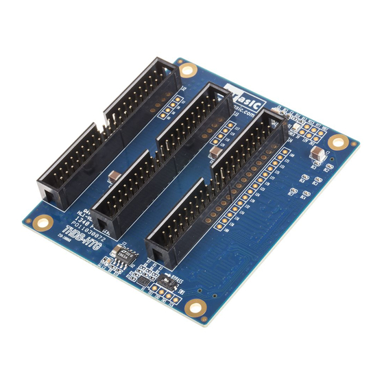
Altera DE2/DE1 expansion headers. Users can connect up to three Altera DE2/DE1 boards (or associated daughter cards) onto a HSTC/HSMC-interfaced host board via a THDB-HTG board. Features Figure 1.1 shows the photo of a THDB-HTG board. The important functions of the THDB-HTG are listed below: •... -
Page 4: Architecture
Architecture Architecture This chapter describes the architecture of the THDB-HTG board, including block diagram and components. Layout and Componets Figure 2.1, Figure 2.2, and Figure 2.3 depict the layout of the board and indicate the locations of the connectors and key components. - Page 5 Architecture 180-pin Female HSTC Connector (J1) Figure 2.2 Back side of the TDRB-HTG board – HSTC version 180-pin Male HSMC Connector (J1) Figure 2.3 Back side of the TDRB-HTG board – HSMC version...
-
Page 6: Block Diagram
Architecture The following components are provided on the THDB-HTG board : • HSTC/HSMC expansion connector (J1) • Expansion prototype connectors (J2,J3,J4) • I2C serial EEPROM (U1) Block Diagram Figure 2.4 shows the block diagram of the THDB-HTG board. HSTC/HSMC Connector... -
Page 7: Board Components
This section describes the HSTC/HSMC connector on the THDB-HTG board There are two options of high speed connector on the THDB-HTG board. One is a 180-pin female HSTC connector for HSTC-interfaced host board such as Altera DE3 board and Terasic PCI board. The other one is a 180-pin male connector for Altera HSMC-interfaced host board. - Page 8 Board Components VCC33 VCC33 HSTCA_CLKOUT_n0 HSTCA_CLKIN_n0 HSMC_CLKOUTn2 HSMC_CLKINn2 HSTCA_CLKOUT_p0 HSTCA_CLKIN_p0 HSMC_CLKINp2 HSMC_CLKOUTp2 HSTCA_TX_n0 HSTCA_RX_n0 HSMC_TX_n16 HSMC_RX_n16 HSTCA_TX_p0 HSTCA_RX_p0 HSMC_RX_p16 HSMC_TX_p16 HSTCA_TX_n1 HSTCA_RX_n1 HSMC_RX_n15 HSMC_TX_n15 HSTCA_TX_p1 HSTCA_RX_p1 HSMC_RX_p15 HSMC_TX_p15 HSTCA_TX_n2 HSTCA_RX_n2 HSMC_TX_n14 HSMC_RX_n14 HSTCA_TX_p2 HSTCA_RX_p2 HSMC_RX_p14 HSMC_TX_p14 HSTCA_TX_n3 HSTCA_RX_n3 HSMC_TX_n13 HSMC_RX_n13 HSTCA_TX_p3 HSTCA_RX_p3 HSMC_TX_p13...
-
Page 9: Expansion Prototype Connectors
This section describes the expansion prototype connectors on the THDB-HTG board. The THDB-HTG board has three expansion prototype connectors (J2, J3, and J4) connected to the HSTC/HSMC connector directly. Each of the connectors has 36 prototyping I/Os and 3.3/5 volts power supply from the HSTC/HSMC interface and on-board regulator. - Page 10 Board Components HSMC_CLKINn2 HSMC_RX_n16 HSMC_CLKINn1 HSMC_RX_n7 HSMC_TXVR_TXn0 HSMC_TXVR_RXn0 HSMC_CLKINp2 HSMC_RX_p16 HSMC_CLKINp1 HSMC_RX_p7 HSMC_TXVR_TXp0 HSMC_TXVR_RXP0 HSMC_RX_n15 HSMC_RX_n6 HSMC_TX_n16 HSMC_TX_n7 HSMC_RX_p15 HSMC_RX_p6 HSMC_TX_p16 HSMC_TX_p7 HSMC_TXVR_TXn1 HSMC_TXVR_RXn1 HSMC_RX_n14 HSMC_RX_n5 HSMC_TX_n15 HSMC_TX_n6 HSMC_TXVR_TXp1 HSMC_TXVR_RXp1 HSMC_RX_p14 HSMC_RX_p5 HSMC_TX_p15 HSMC_TX_p6 HSMC_RX_n13 HSMC_RX_n4 HSMC_TX_n14 HSMC_TX_n5 HSMC_TXVR_RXn2 HSMC_TXVR_TXn2 HSMC_RX_p13 HSMC_RX_p4 HSMC_TX_p14...
- Page 11 Board Components Table 3.1 Pin mappings of the expansion prototype connector J2 Expansion Prototype Connector 1 – J2 J2 Pin J1 Pin J1 (HSTC Version) Signal J1 (HSMC Version) Signal DE2/DE1 Number Number Name Name GPIO Sgnal Name HSTC_CLKIN_n0 HSMC_CLKIN_n2 GPIO0 HSTC_RX_n0 HSMC_RX_n16...
- Page 12 Board Components Table 3.2 Pin mappings of the expansion prototype connector J3 Expansion Prototype Connector 1 – J3 J3 Pin J1 Pin J1 (HSTC Version) Signal J1 (HSMC Version) Signal DE2/DE1 Number Number Name Name GPIO Sgnal Name HSTC_CLKIN_n1 HSMC_CLKIN_n1 GPIO0 HSTC_RX_n9 HSMC_RX_n7...
- Page 13 Board Components Table 3.3 Pin mappings of the expansion prototype connector J4 Expansion Prototype Connector 1 – J4 J4 Pin J1 Pin J1 (HSTC Version) Signal J1 (HSMC Version) Signal DE2/DE1 Number Number Name Name GPIO Sgnal Name HSTC_TX_n18 GPIO0 HSTC_RX_n18 GPIO1 HSTC_TX_p18...
-
Page 14: Prototyping Area
Board Components Prototyping Area The THDB-HTG board provides users a prototyping area for signal measurement or debug. These prototyping points are connected to the HSTC/HSMC connector directly. Detailed I/O maps for HSTC and HSMC version are provided to help users locate the corresponding prototyping points, as shown in Figure 3.4 and Figures 3.5, respectively. -
Page 15: Jtag Switch
JTAG signal from host board to form a close loop of JTAG chain. For example, if users connect a THDB-HTG with Altera DE3 board, this switch must be turned on, or the Stratix III FPGA device will not be detected because the JTGA chain is not a close loop on DE3 board. -
Page 16: Power Supply
HSTC_SCL J1-132 U1-7 U1-8 VCC33 (3.3 volts) Power Supply 1-11 This section describes the power supply on the THDB-HTG board. The power distribution on the THDB-HTG board is shown in Figure 3.7. Regulator Expansion Prototype HSTC/HSMC Connectors Connector J2~J4 EEPROM 3.3V... -
Page 17: Demonstration
This section describes how to use the THDB-HTG board with a Cyclone III Starter Board. Figure 4.1 illustrates how the THDB-HTG board is connected to the Cyclone III starter board. Users need to pay extra attention to the following two points: Observe the orientation of the HSMC connector when connecting the THDB-HTG to the Cyclone III Starter Board. -
Page 18: Connecting Thdb-Htg Board To Altera De3 Board
1-13 This section describes how to use the THDB-HTG board with Altera DE3 Board. Figure 4.2 illustrates how the THDB-HTG board is connected to the Altera DE3 board. Users need to pay extra attention to the following three points: THDB-HTG board can be connected to any of the HSTC connectors J1, J3, J5, and J7 on the DE3 board. -
Page 19: Appendix
Revision History 1-15 Date Change Log DEC 23, 2009 Initial Version Always Visit THDB-HTG Webpage for New Main board 1-16 We will be continuing providing interesting examples and labs on our THDB-HTG webpage. Please visit www.altera.com or HTG.terasic.com for more information. - Page 20 All rights reserved. No part of this schematic design may be reproduced, duplicated, or used without the prior written permission of Terasic. No part of this schematic design may be reproduced, duplicated, or used without the prior written permission of Terasic.
Need help?
Do you have a question about the THDB-HTG and is the answer not in the manual?
Questions and answers