Terasic de10-nano User Manual
Cyclone v soc with dual-core arm cortex-a9
Hide thumbs
Also See for de10-nano:
- Getting started manual (35 pages) ,
- Quick start manual (4 pages) ,
- Getting started manual (24 pages)
Table of Contents
Advertisement
Advertisement
Table of Contents

Related Manuals for Terasic de10-nano


Summary of Contents for Terasic de10-nano
- Page 1 DE10-Nano www.terasic.com User Manual May 31, 2017...
-
Page 2: Table Of Contents
2.1 Layout and Components 2.2 Block Diagram of the DE10-Nano Board Chapter 3 Using the DE10-Nano Board 3.1 Settings of FPGA Configuration Mode 3.2 Configuration of Cyclone V SoC FPGA on DE10-Nano 3.3 Board Status Elements 3.4 Board Reset Elements 3.5 Clock Circuitry 3.6 Peripherals Connected to the FPGA... - Page 3 Chapter 5 Examples For FPGA 5.1 DE10-Nano Factory Configuration 5.2 ADC Reading 5.3 HDMI TX 5.4 DDR3_VIP 5.5 DDR3_RTL 5.6 Nios II Access HPS DDR3 Chapter 6 Examples for HPS SoC 6.1 Hello Program 6.2 Users LED and KEY 6.3 I2C Interfaced G-sensor 6.4 Setup USB Wi-Fi Dongle...
-
Page 4: Chapter 1 De10-Nano Development Kit
DDR3 memory, analog to digital capabilities, Ethernet networking, and much more that promise many exciting applications. The DE10-Nano Development Kit contains all the tools needed to use the board in conjunction with a computer that runs the Microsoft Windows XP or later. -
Page 5: De10-Nano System Cd
Card (Installed) Four Silicon Footstands The DE10-Nano System CD contains all the documents and supporting materials associated with DE10-Nano, including the user manual, system builder, reference designs, and device datasheets. Users can download this system CD from the link: http://de10-nano.terasic.com/cd. -
Page 6: Chapter 2 Introduction Of The De10-Nano Board
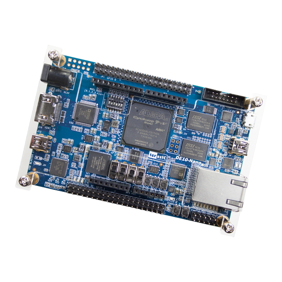
Figure 2-1 Figure 2-2 shows a photograph of the board. It depicts the layout of the board and indicates the location of the connectors and key components. Figure 2-1 DE10-Nano development board (top view) DE10-Nano www.terasic.com User Manual May 31, 2017... - Page 7 Figure 2-2 DE10-Nano development board (bottom view) The DE10-Nano board has many features that allow users to implement a wide range of designed circuits, from simple circuits to various multimedia projects. The following hardware is provided on the board: FPGA ...
- Page 8 Accelerometer (I2C interface + interrupt) UART to USB, USB Mini-B connector Warm reset button and cold reset button One user button and one user LED LTC 2x7 expansion header DE10-Nano www.terasic.com User Manual May 31, 2017...
- Page 9 Cyclone V SoC FPGA device to provide maximum flexibility for users. Users can configure the FPGA to implement any system design. Detailed information about Figure 2-3 are listed below. Figure 2-3 Block diagram of DE10-Nano DE10-Nano www.terasic.com User Manual May 31, 2017...
- Page 10 One LTC connector (one Serial Peripheral Interface (SPI) Master ,one I2C and one GPIO interface ) HDMI TX, compatible with DVI v1.0 and HDCP v1.4 12-Bit Resolution, 500Ksps Sampling Rate. SPI Interface. 8-Channel Analog Input. Input Range : 0V ~ 4.096V. DE10-Nano www.terasic.com User Manual May 31, 2017...
- Page 11 3 user Keys (FPGA x2, HPS x1) 4 user switches (FPGA x4) 9 user LEDs (FPGA x8, HPS x 1) 2 HPS reset buttons (HPS_RESET_n and HPS_WARM_RST_n) G-Sensor on HPS 5V DC input DE10-Nano www.terasic.com User Manual May 31, 2017...
- Page 12 Board his chapter provides an instruction to use the board and describes the peripherals. When the DE10-Nano board is powered on, the FPGA can be configured from EPCS or HPS. The MSEL[4:0] pins are used to select the configuration scheme. It is implemented as a...
- Page 13 EPCS, which is pre-programmed with the default code. If developers using the "Linux LXDE Desktop" SD Card image, the MSEL[4:0] needs to be set to “01010” before the board is powered on. MSEL Pin Settings for FPGA Configure of DE10-Nano Board Table 3-2 SW10.1 SW10.2...
- Page 14 In addition, the DE10-Nano has one external JTAG Header (J8) reserved for users to connect to JTAG chain of the DE10-Nano via external blaster. The J8 header is not installed, so users need to solder a 2.54mm 2x7 male pin header if it is necessary.
- Page 15 FPGA is programmed in JTAG mode step by step. Open the Quartus II programmer, please Choose Tools > Programmer. The Programmer window opens. Please click “Hardware Setup”, as circled in Figure 3-3. Figure 3-3 Programmer Window DE10-Nano www.terasic.com User Manual May 31, 2017...
- Page 16 “Close” to close the window. See Figure 3-4. Figure 3-4 Hardware Setting Return to the Quartus II programmer and click “Auto Detect”, as circled in Figure 3-5 Figure 3-5 Detect FPGA device in JTAG mode DE10-Nano www.terasic.com User Manual May 31, 2017...
- Page 17 “OK” to close the window, as circled in Figure 3-6. Figure 3-6 Select 5CSEBA6 device Both FPGA and HPS are detected, as shown in Figure 3-7. Figure 3-7 FPGA and HPS detected in Quartus programmer DE10-Nano www.terasic.com User Manual May 31, 2017...
- Page 18 Figure 3-8 Open the .sof file to be programmed into the FPGA device Select the .sof file to be programmed, as shown in Figure 3-9. Figure 3-9 Select the .sof file to be programmed into the FPGA device DE10-Nano www.terasic.com User Manual May 31, 2017...
- Page 19 Click “Program/Configure” check box and then click “Start” button to download the .sof file into the FPGA device, as shown in Figure 3-10. Figure 3-10 Program.sof file into the FPGA device DE10-Nano www.terasic.com User Manual May 31, 2017...
- Page 20 Configure the FPGA in AS Mode The DE10-Nano board uses a serial configuration device (EPCS128) to store configuration data for the Cyclone V SoC FPGA. This configuration data is automatically loaded from the serial configuration device chip into the FPGA when the board is powered up.
- Page 21 In addition to the 9 LEDs that FPGA/HPS device can control, there are 6 indicators which can indicate the board status (See Figure 3-12), please refer the details in Table 3-3 Figure 3-12 LED Indicators on DE10-Nano LED Indicators Table 3-3 Board Reference LED Name...
- Page 22 There are two HPS reset buttons on DE10-Nano, HPS (cold) reset and HPS warm reset, as shown in Figure 3-13. Table 3-4 describes the purpose of these two HPS reset buttons. Figure 3-14 is the reset tree for DE10-Nano. Figure 3-13 HPS cold reset and warm reset buttons on DE10-Nano...
- Page 23 Figure 3-14 HPS reset tree on DE10-Nano board Figure 3-15 shows the default frequency of all external clocks to the Cyclone V SoC FPGA. A clock generator is used to distribute clock signals with low jitter. The two 50MHz clock signals connected to the FPGA are used as clock sources for user logic.
- Page 24 Figure 3-15 Block diagram of the clock distribution on DE10-Nano Pin Assignment of Clock Inputs Table 3-5 Signal Name FPGA Pin No. Description I/O Standard FPGA_CLK1_50 PIN_V11 50 MHz clock input 3.3V FPGA_CLK2_50 PIN_Y13 50 MHz clock input 3.3V FPGA_CLK3_50 PIN_E11 50 MHz clock input (share with FPGA_CLK1_50) 3.3V...
- Page 25 Figure 3-16 Connections between the push-buttons and the Cyclone V SoC FPGA Pushbutton depressed Pushbutton released Before Debouncing Schmitt Trigger Debounced Figure 3-17 Switch debouncing DE10-Nano www.terasic.com User Manual May 31, 2017...
- Page 26 LED on or off, respectively. Figure 3-19 shows the connections between LEDs and Cyclone V SoC FPGA. Table 3-6, Table 3-7 Table 3-8 list the pin assignment of user push-buttons, switches, and LEDs. DE10-Nano www.terasic.com User Manual May 31, 2017...
- Page 27 Description I/O Standard LED[0] PIN_W15 LED [0] 3.3V LED[1] PIN_AA24 LED [1] 3.3V LED[2] PIN_V16 LED [2] 3.3V LED[3] PIN_V15 LED [3] 3.3V LED[4] PIN_AF26 LED [4] 3.3V LED[5] PIN_AE26 LED [5] 3.3V DE10-Nano www.terasic.com User Manual May 31, 2017...
- Page 28 PIN_AG18 GPIO_1[28] GPIO_1[29] PIN_AH18 PIN_AB25 GPIO_0[30] GPIO_0[31] PIN_AB26 PIN_AF18 GPIO_1[30] GPIO_1[31] PIN_AF20 PIN_Y11 GPIO_0[32] GPIO_0[33] PIN_AA26 PIN_AG15 GPIO_1[32] GPIO_1[33] PIN_AE20 PIN_AA13 GPIO_0[34] GPIO_0[35] PIN_AA11 PIN_AE19 GPIO_1[34] GPIO_1[35] PIN_AE17 Figure 3-20 GPIO Pin Arrangement DE10-Nano www.terasic.com User Manual May 31, 2017...
- Page 29 GPIO Connection 0[26] 3.3V GPIO_0[27] PIN_W14 GPIO Connection 0[27] 3.3V GPIO_0[28] PIN_Y18 GPIO Connection 0[28] 3.3V GPIO_0[29] PIN_Y17 GPIO Connection 0[29] 3.3V GPIO_0[30] PIN_AB25 GPIO Connection 0[30] 3.3V GPIO_0[31] PIN_AB26 GPIO Connection 0[31] 3.3V DE10-Nano www.terasic.com User Manual May 31, 2017...
- Page 30 GPIO Connection 1[30] 3.3V GPIO_1[31] PIN_AF20 GPIO Connection 1[31] 3.3V GPIO_1[32] PIN_AG15 GPIO Connection 1[32] 3.3V GPIO_1[33] PIN_AE20 GPIO Connection 1[33] 3.3V GPIO_1[34] PIN_AE19 GPIO Connection 1[34] 3.3V GPIO_1[35] PIN_AE17 GPIO Connection 1[35] 3.3V DE10-Nano www.terasic.com User Manual May 31, 2017...
- Page 31 The 16 GPIO pins are provided to the Arduino Header for digital I/O. Table 3-11 lists the all the pin assignments of the Arduino Uno connector (digital), signal names relative to the Cyclone V SoC FPGA. DE10-Nano www.terasic.com User Manual May 31, 2017...
- Page 32 Besides 16 pins for digital GPIO, there are also 6 analog inputs on the Arduino Uno R3 Expansion Header (ADC_IN0 ~ ADC_IN5). Consequently, we use ADC LTC2308 from Linear Technology on the board for possible future analog-to-digital applications. We will introduce in the next section. DE10-Nano www.terasic.com User Manual May 31, 2017...
- Page 33 FPGA, 2x5 header, Arduino Analog input, and the A/D converter. More information about the A/D converter chip is available in its datasheet. It can be found on manufacturer’s website or in the directory \Datasheet\ADC of DE10-Nano system CD. DE10-Nano www.terasic.com...
- Page 34 FPGA Pin No. Description I/O Standard ADC_CONVST PIN_U9 Conversion Start 3.3V ADC_SCK PIN_V10 Serial Data Clock 3.3V ADC_SDI PIN_AC4 Serial Data Input (FPGA to ADC) 3.3V ADC_SDO PIN_AD4 Serial Data Out (ADC to FPGA) 3.3V DE10-Nano www.terasic.com User Manual May 31, 2017...
- Page 35 Datasheets\HDMI folder on the Kit System CD. Table 3-13 lists the HDMI Interface pin assignments and signal names relative to the Cyclone V SoC device. Figure 3-24 Connections between the Cyclone V SoC FPGA and HDMI Transmitter Chip DE10-Nano www.terasic.com User Manual May 31, 2017...
- Page 36 3.3-V HDMI_MCLK PIN_U11 Audio Reference Clock Input 3.3-V HDMI_LRCLK PIN_T11 Audio Left/Right Channel Signal Input 3.3-V HDMI_SCLK PIN_T12 I2S Audio Clock Input 3.3-V I2C_SCL PIN_U10 I2C Clock 3.3-V I2C_SDA PIN_AA4 I2C Data 3.3-V DE10-Nano www.terasic.com User Manual May 31, 2017...
- Page 37 The pin assignment associated to Gigabit Ethernet interface is listed in Table 3-15. More information about the KSZ9031RN PHY chip and its datasheet, as well as the application notes, which are available on the manufacturer’s website. DE10-Nano www.terasic.com User Manual May 31, 2017...
- Page 38 RJ45 connector. The state and definition of LEDG and LEDY are listed in Table 3-16. For instance, the connection from board to Gigabit Ethernet is established once the LEDG lights on. DE10-Nano www.terasic.com User Manual May 31, 2017...
- Page 39 HW flow control signals. The physical interface is implemented by UART-USB onboard bridge from a FT232R chip to the host with an USB Mini-B connector. More information about the chip is available on the manufacturer’s website, or in the directory \Datasheets\UART_TO_USB of DE10-Nano system CD. Figure 3-25 shows the connections between the HPS, FT232R chip, and the USB Mini-B connector.
- Page 40 HPS_DDR3_A[12] PIN_D24 HPS DDR3 Address[12] SSTL-15 Class I HPS_DDR3_A[13] PIN_C24 HPS DDR3 Address[13] SSTL-15 Class I HPS_DDR3_A[14] PIN_G23 HPS DDR3 Address[14] SSTL-15 Class I HPS_DDR3_BA[0] PIN_A27 HPS DDR3 Bank Address[0] SSTL-15 Class I DE10-Nano www.terasic.com User Manual May 31, 2017...
- Page 41 SSTL-15 Class I HPS_DDR3_DQ[25] PIN_R25 HPS DDR3 Data[25] SSTL-15 Class I HPS_DDR3_DQ[26] PIN_AA28 HPS DDR3 Data[26] SSTL-15 Class I HPS_DDR3_DQ[27] PIN_W26 HPS DDR3 Data[27] SSTL-15 Class I HPS_DDR3_DQ[28] PIN_R24 HPS DDR3 Data[28] SSTL-15 Class I DE10-Nano www.terasic.com User Manual May 31, 2017...
- Page 42 HPS_DDR3_RAS_n PIN_A25 DDR3 Row Address Strobe SSTL-15 Class I HPS_DDR3_RESET_n PIN_V28 HPS DDR3 Reset SSTL-15 Class I HPS_DDR3_WE_n PIN_E25 HPS DDR3 Write Enable SSTL-15 Class I HPS_DDR3_RZQ PIN_D25 For output drive calibration 1.5V DE10-Nano www.terasic.com User Manual May 31, 2017...
- Page 43 The board supports Micro SD card interface with x4 data lines. It serves not only an external storage for the HPS, but also an alternative boot option for DE10-Nano board. Figure 3-27 shows signals connected between the HPS and Micro SD card socket.
- Page 44 HPS USB_DATA[7] 3.3V HPS_USB_DIR PIN_E5 Direction of the Data Bus 3.3V HPS_USB_NXT PIN_D5 Throttle the Data 3.3V HPS_USB_RESET PIN_H12 HPS USB PHY Reset 3.3V HPS_USB_STP PIN_C5 Stop Data Stream on the Bus 3.3V DE10-Nano www.terasic.com User Manual May 31, 2017...
- Page 45 I2C interface. The I2C address of G-sensor is 0xA6/0xA7. More information about this chip can be found in its datasheet, which is available on manufacturer’s website or in the directory \Datasheet\G-Sensor folder of DE10-Nano system CD. Figure 3-29 shows the connections between the HPS and G-sensor.
- Page 46 3.3V HPS_I2C1_SDAT PIN_A21 HPS I2C1 Data 3.3V HPS_SPIM_CLK PIN_C19 SPI Clock 3.3V HPS_SPIM_MISO PIN_B19 SPI Master Input/Slave Output 3.3V HPS_SPIM_MOSI PIN_B16 SPI Master Output /Slave Input 3.3V HPS_SPIM_SS PIN_C16 SPI Slave Select 3.3V DE10-Nano www.terasic.com User Manual May 31, 2017...
- Page 47 DE10-Nano System Builder. The DE10-Nano System Builder is a Windows-based utility. It is designed to help users create a Quartus II project for DE10-Nano within minutes. The generated Quartus II project files include: ...
- Page 48 DE10-Nano under the DE10-Nano System Builder. The design flow is illustrated in Figure The DE10-Nano System Builder will generate two major files, a top-level design file (.v) and a Quartus II setting file (.qsf) after users launch the DE10-Nano System Builder and create a new project according to their design requirements.
- Page 49 This section provides the procedures in details on how to use the DE10-Nano System Builder. Install and Launch the DE10-Nano System Builder The DE10-Nano System Builder is located in the directory: “Tools\SystemBuilder” of the DE10-Nano System CD. Users can copy the entire folder to a host computer without installing the utility.
- Page 50 Enter the project name in the circled area, as shown in Figure 4-3. The project name typed in will be assigned automatically as the name of your top-level design entity. Figure 4-3 Enter the project name DE10-Nano www.terasic.com User Manual May 31, 2017...
-
Page 51: System Configuration
4-4. Each component onboard is listed and users can enable or disable one or more components at will. If a component is enabled, the DE10-Nano System Builder will automatically generate its associated pin assignment, including the pin name, pin location, pin direction, and I/O standard. - Page 52 GPIO Expansion If users connect any Terasic GPIO-based daughter card to the GPIO connector(s) on DE10-Nano, the DE10-Nano System Builder can generate a project that include the corresponding module, as shown in Figure 4-5. It will also generate the associated pin assignment automatically, including pin name, pin location, pin direction, and I/O standard.
- Page 53 Project Setting Management The DE10-Nano System Builder also provides the option to load a setting or save users’ current board configuration in .cfg file, as shown in Figure 4-6. Figure 4-6 Project Settings DE10-Nano www.terasic.com User Manual May 31, 2017...
- Page 54 Project Generation When users press the Generate button, the DE10-Nano System Builder will generate the corresponding Quartus II files and documents, as listed in Table 4-1: Files generated by the DE10-Nano System Builder Table 4-1 Filename Description <Project name>.v Top level Verilog HDL file for Quartus II <Project name>.qpf...
-
Page 55: Peripherals Connected To The Fpga
NO space. Otherwise it will lead to error in Nios II. Note Quartus II v16.0 or later is required for all DE10-Nano demonstrations to support Cyclone V SoC device. The DE10-Nano board has a default configuration bit-stream pre-programmed, which demonstrates some of the basic features on board. - Page 56 0 and 4.096V. The 12-bit voltage measurement is displayed on the NIOS II console. Figure 5-2 shows the block diagram of this demonstration. If the input voltage is -2.0V ~ 2.0V, a pre-scale circuit can be used to adjust it to 0 ~ 4V. DE10-Nano www.terasic.com User Manual May 31, 2017...
- Page 57 Nios II console. Figure 5-3 Pin distribution of the 2x5 Header for the ADC DE10-Nano www.terasic.com User Manual May 31, 2017...
- Page 58 System Requirements The following items are required for this demonstration. DE10-Nano board x1 Trimmer Potentiometer x1 Wire Strip x3 Demonstration File Locations Hardware project directory: \ADC Bitstream used: DE10_NANO_ADC.sof Software project directory: \ADC\software ...
- Page 59 I2C design. A set of built-in video patterns and audio serial data will be sent to the HDMI transmitter to drive the HDMI display with speaker. Users can hear the beeping sound from the speaker when SW0 is set to 1 on the DE10-Nano board. The resolution can be switched by pressing KEY1.
- Page 60 LCD monitor. The pattern is composed in the way of 24-bit RGB 4:4:4 (RGB888 per color pixel without sub-sampling) color encoding, which corresponds to the parallel encoding format defined in Table 5-1 of the "ADV7513 Hardware User's Guide," as shown below. DE10-Nano www.terasic.com User Manual May 31, 2017...
-
Page 61: Uart
Demonstration Setup and Instructions Please make sure both Quartus II and USB-Blaster II driver are installed on the host Connect the DE10-Nano board to the LCD monitor through a HDMI cable. Power on the DE10-Nano board ... - Page 62 Figure 5-8. The SW0 is used to enable/disable the sound output on the DE10-Nano board. When you switch the SW0 button to an upper position, you will hear a "beep" sound from the speaker of the HDMI display.
-
Page 63: Ddr3 Memory
VIP (Video and Image Processing) suite. Before running the FPGA demo, users have to boot the DE10-Nano from HPS to execute the Preloader, Bootloader, and soc_system.rbf programs from the microSD card for HPS and DDR3 initialization. The required microSD card image, terasic_hps_ddr3.img, is provided in the DE10-Nano... - Page 64 In the FPGA site, the terasic_hps_ddr3 sub-system, provided by Terasic, is used to provide a bridge between the FPGA and the HPS DDR3. The VIP suite is used to implement the pattern generator, and the HPS DDR3 is used as a buffer for the VIP Frame Buffer II. The frame buffer accesses the DDR3 through the FPGA-to-HPS interface and SDRAM Controller.
- Page 65 You can also configure the FGPA through the usb-blaster JTAG interface. The FPGA can also be configured by Bootloader in the microSD card. When the DE10-Nano is booted from HPS, the Bootloader will configure the FPGA by the configuration file soc_system.rbf which is also provided in the microSD card.
- Page 66 Program terasic_hps_ddr3.img into a microSD card Insert the microSD card into the DE10-Nano board Make sure the MSEL[4:0] is set to 01010 Connect a mini-USB cable to UB2 port of DE10-Nano and the host PC DE10-Nano www.terasic.com User Manual May 31, 2017...
- Page 67 Power on the DE10-Nano board Wait until HPS LED0 is lighted. This indicate the DDR3 is ready Launch the "test.bat" batch file from the "\DDR3_VIP\demo_batch" folder. After the programming and configuration are successful, the screen should look like the one...
- Page 68 In this demonstration case, FPGA is configured by Bootloader which read the configuration file soc_system.rbf from the microSD card. In this demonstration setup, no USB cable is required. Connect the DE10-Nano board to the LCD monitor through a HDMI cable Programming terasic_hps_ddr3.img into a microSD card ...
- Page 69 DDR3 on the HPS site. In this case, the RTL code can access the DDR3 through the Avalon memory-mapped interface. Before running the FPGA demo, users have to make the DE10-Nano boot from HPS to execute the Preloader, Bootloader, and soc_system.rbf programs from the microSD card for the HPS and DDR3 initialization.
- Page 70 In the FPGA site, the terasic_hps_ddr3 sub-system, provided by Terasic, is used to provide a bridge between FPGA and HPS DDR3. Avalon_bus_RW_test is a memory test module. It performs memory write and read back verification. It accesses the DDR3 through the FPGA-to-HPS interface and SDRAM Controller.
- Page 71 Besides configuring FGPA through the usb-blaster JTAG interface. The FPGA can also be configured via Bootloader in the microSD card. When DE10-Nano is booted from HPS, the Bootloader will configure the FPGA by the configuration file soc_system.rbf which is also provided in the microSD card.
- Page 72 Please followbelow instructions to configure FPGA with .sof file through the usb-blaster JTAG interface to performance the demonstration. Make sure both Quartus II and USB-Blaster II driver are installed on the host PC. Program terasic_hps_ddr3.img into a microSD card. DE10-Nano www.terasic.com User Manual May 31, 2017...
- Page 73 Insert the microSD card into the DE10-Nano board. Make sure the MSEL[4:0] is set to 01010. Connect a mini-USB cable to UB2 port of DE10-Nano and the host PC. Power on the DE10-Nano board Wait the HPS LED0 is lighted. This indicates the DDR3 is ready.
- Page 74 Programming terasic_hps_ddr3.img into a microSD card. Copy the RBF file soc_system.rbf into the microSD card. Insert the microSD card into the DE10-Nano board. Make sure the MSEL[4:0] is set to 01010. Power on the DE10-Nano board.
- Page 75 F2H SDRAM Interface setting in the HPS component in the Qsys Figure 5-19 tool. The interface type Avalon-MM Bidrectional is selected and the data width 32-bit is used. Figure 5-19 F2H SDRAM Interface Setting System Requirements DE10-Nano www.terasic.com User Manual May 31, 2017...
- Page 76 Make sure MSEL[4:0] is set to 01010 Connect another mini-usb cable to the J4 on the DE10-Nano and the host PC for HPS/Linux boot. Open the putty and power up the board. Before the count down finishes, hit any key to...
- Page 77 Figure 5-20 HPS U-Boot Terminal DE10-Nano www.terasic.com User Manual May 31, 2017...
- Page 78 Figure 5-23 Figure 5-23Take The F2H SDRAM Port Out Of Reset Connect another mini-usb cable to the J13 on the DE10-Nano and the host PC for running the Nios2 code. DE10-Nano www.terasic.com User Manual...
- Page 79 Execute the test.bat in the demo_batch folder. The Nios2 code will run to test the 128M memory start at 0x20000000 in the DDR3 as in Figure 5-24. Figure 5-24 Nios2 Test The DDR3 Memory DE10-Nano www.terasic.com User Manual May 31, 2017...
-
Page 80: G-Sensor
HPS interface on DE10-Nano board such as users LED/KEY, I2C interfaced G-sensor. All the associated files can be found in the directory Demonstrations/SOC of the DE10-Nano System CD. Please refer to Chapter 5 "Running Linux on the DE10-Nano board" from the Getting_Started_Guide.pdf to run Linux on DE10-Nano board. - Page 81 Program File The main program for the Hello World demonstration is: Makefile A Makefile is required to compile a project. The Makefile used for this demo is: DE10-Nano www.terasic.com User Manual May 31, 2017...
- Page 82 Launch PuTTY to establish the connection between the UART port of DE10-Dano board and the host PC. Type "root" with the password “terasic” to login LXDE Linux. Type "./my_first_hps" in the UART terminal of PuTTY to start the program, and the "Hello World!"...
-
Page 83: Users Led And Key
GPIO1 controller in HPS. The behavior of GPIO controller is controlled by the register in GPIO controller. The registers can be accessed by application software through the memory-mapped device driver, which is built into SoC Linux. Figure 6-1 Block diagram of GPIO demonstration DE10-Nano www.terasic.com User Manual May 31, 2017... - Page 84 IO pin in the associated GPIO controller and so on. The value "1" in the register bit indicates the I/O direction is output, while the value "0" in the register bit indicates the I/O direction is input. DE10-Nano www.terasic.com User Manual...
- Page 85 64KB size. The registers of the GPIO1 controller are mapped to the base address 0xFF708000 with 4KB size, and the registers of the GPIO2 controller are mapped to the base address 0xFF70A000 with 4KB size, as shown in Figure 6-3. Figure 6-3 GPIO address map DE10-Nano www.terasic.com User Manual May 31, 2017...
-
Page 86: Software Api
The program must include the following header files to use the above API to access the registers of GPIO controller. #include <stdio.h> #include <unistd.h> #include <fcntl.h> #include <sys/mman.h> #include "hwlib.h" #include "socal/socal.h" #include "socal/hps.h" #include "socal/alt_gpio.h" DE10-Nano www.terasic.com User Manual May 31, 2017... - Page 87 LED and KEY Control Figure 6-4 shows the HPS users LED and KEY pin assignment for the DE10-Nano board. The LED is connected to HPS_GPIO53 and the KEY is connected to HPS_GPIO54. They are controlled by the GPIO1 controller, which also controls HPS_GPIO29 ~ HPS_GPIO57.
- Page 88 Demonstration Source Code Build tool: SoC EDS V16.0 Project directory: \Demonstration\SoC\hps_gpio Binary file: hps_gpio Build command: make ('make clean' to remove all temporal files) Execute command: ./hps_gpio DE10-Nano www.terasic.com User Manual May 31, 2017...
- Page 89 Launch PuTTY to establish the connection between the UART port of DE10-Dano board and the host PC. Type "root" with the password “terasic” to login LXDE Linux. Type "./hps_gpio " in the UART terminal of PuTTY to start the program.
-
Page 90: Function Block Diagram
The G-sensor on the DE10-Nano board is connected to the I2C0 controller in HPS. The G-Sensor I2C 7-bit device address is 0x53. The system I2C bus driver is used to access the register files in the G-sensor. - Page 91 G-sensor Control The ADI ADXL345 provides I2C and SPI interfaces. I2C interface is selected by setting the CS pin to high on the DE10-Nano board. The ADI ADXL345 G-sensor provides user-selectable resolution up to 13-bit ± 16g. The resolution can be configured through the DATA_FORAMT(0x31) register. The data format in this demonstration is configured as: ...
- Page 92 Launch PuTTY to establish the connection between the UART port of DE10-Dano board and the host PC. Type "root" with the password “terasic” to login LXDE Linux. Execute "./gsensor" in the UART terminal of PuTTY to start the G-sensor polling.
-
Page 93: System Diagram
Figure 6-9 System diagram of USB Wi-Fi dongle Wi-Fi Setup Procedure Connect a USB cable to the USB-to-UART connector (J4) on the DE10-Nano board and the host PC. Use a USB OTG cable to connect the USB Wi-Fi Dongle and the micro USB port on the DE10-Nano. - Page 94 PC. Type "root" with the password "terasic" to login to the LXDE Linux. Type "ifconfig wlan0 up" in the UART terminal of PuTTY to start wlan0 network interface. Type "iwlist wlan0 scan | grep ESSID" in the UART terminal to search nearby Wi-Fi AP.
- Page 95 Type "ifconfig wlan0" in the UART terminal to confirm an IP Address is assigned to wlan0 interface. Make sure Wi-Fi AP is connected to the internet. Type "ping -c 4 www.terasic.com" in the UART terminal to check internet connection status. If 0% packet loss is reported, it means the connection is good.
-
Page 96: Query Internet Time
Internet. The time information will be shown on the UART terminal with the format HH:MM:SS. The DE10-Nano connects to Ethernet through wire RJ45 Port or wireless Wi-Fi USB-Dongle. For details about how to setup the Wi-Fi USB-Dongle, please refer to the chapter 6.4 Setup USB Wi-Fi... - Page 97 Launch PuTTY to establish the connection between the UART port of DE10-Nona board and the host PC. Type "root" with the password “terasic” to login LXDE Linux. Type "./NET_Time" in the UART terminal of PuTTY to start the program.
-
Page 98: Ghrd Project
Basic C coding and compiling skill Skill to Create a Linux Boot SD-Card for DE10-Nano with a given image file Skill to boot Linux from SD-Card on DE10-Nano Skill to cope files into Linux file system on DE10-Nano Basic Linux command operation skill DE10-Nano www.terasic.com... - Page 99 Before starting this tutorial, please note that the following items are required to complete the demonstration project: Terasic DE10-Nano FPGA board, includes Mini USB Cable for UART terminal Micros SD-Card, at 4GB minimum Micros SD-Card Card Reader ...
- Page 100 HPS-to-FPGA bridge. This Demo introduces to users how to use the HPS/ARM to communicate with FPGA. This project includes GHRD project for the DE10-Nano one ARM C Project which demonstrates how HPS/ARM program controls the green LEDs connected to FPGA.
- Page 101 The term GHRD is short for Golden Hardware Reference Design. The GRD project provide by Terasic DE10-Nano development board located folder: CD-ROM\Demonstration\SOC_FPGA\ DE10_NANO_SoC_GHRD. The project consists of the following components: ARM Cortex™-A9 MPCore HPS Two user push-button inputs ...
- Page 102 All the Avalon Conduit signals of these peripherals are connected to the I/O pins of the SoCFPGA Figure 7-3. on DE10-Nano board as shown in the Figure 7-3 Connection in the top design In the Qsys tool, click the menu item “GenerateGenerate…” to generate source code for the system and then close the Qsys tool.
- Page 103 DE10_NANO_SoC_GHRD.sof is generated in the DE10_NANO_SoC_GHRD\output_files folder. Users can use this file to configure FPGA by Quartus Programming through the DE10-Nano on-board USB-Blaster II. This section introduces how to design an ARM C program to control the led_pio PIO controller.
- Page 104 Based on the rule, the virtual address of led_pio can be calculated by adding the below two offset addresses to virtual_base. Offset address of Lightweight HPS-to-FPGA AXI bus relative to HPS base address Offset address of Pio_led relative to Lightweight HPS-to-FPGA AXI bus DE10-Nano www.terasic.com User Manual May 31, 2017...
-
Page 105: Led Control
PIO Core. For led control, we just need to write output value to the offset 0 register relative to based address 0x3000. Because the led on DE10-Nano is high active, writing a value 0x00000000 to the offset 0 register will turn off all of the DE10-Dano eight green LEDs. - Page 106 Main Program In the main program, the LED is controlled to perform LED light sifting operation as shown in Figure 7-8. When finishing 60 times of shift cycle, the program will be terminated. DE10-Nano www.terasic.com User Manual May 31, 2017...
- Page 107 SoC EDS. In the Makefile, ARM-linux cross-compile also be specified. Figure 7-9 Makefile content To compile the project, type “make” in the command shell as shown in Figure 7-10. Then, type “ls” to check the generated ARM execution file “HPS_FPGA_LED”. DE10-Nano www.terasic.com User Manual May 31, 2017...
- Page 108 DE10_NANO_SoC_GHRD.sof generated in previous chapter. The LED0 will flash as the heat beat of the FPGA. Then, type “./HPS_FPGA_LED” to launch the ARM program. The LED[7..1] on DE10-Nano will be expected to perform 60 times of LED light shift operation, and then the program is terminated.
-
Page 109: Chapter 8 Programming The Epcs Device
The FPGA should be set to AS x1 mode i.e. MSEL[4..0] = “10010” to use the Flash as a FPGA configuration device, as shown in Figure 8-1. Figure 8-1 DIP switch (SW10) setting of Active Serial (AS) mode DE10-Nano www.terasic.com User Manual May 31, 2017... - Page 110 3. Choose EPCS128 from the Configuration device field. 4. Choose Active Serial from the Mode filed. 5. Browse to the target directory from the File name field and specify the name of output file. DE10-Nano www.terasic.com User Manual May 31, 2017...
- Page 111 Figure 8-3 Dialog of “Convert Programming Files” 7. Click Add File. 8. Select the .sof to be converted to a .jic file from the Open File dialog. 9. Click Open and the Convert Programming Files page will appear. DE10-Nano www.terasic.com User Manual May 31, 2017...
- Page 112 10. Click on the Flash Loader and click Add Device, as shown in Figure 8-4. Figure 8-4 Click on the “Flash Loader” DE10-Nano www.terasic.com User Manual May 31, 2017...
- Page 113 EPCS, as shown in Figure 8-5. Figure 8-5 “Select Devices” page 12. Click OK and the Convert Programming Files page will appear, as shown in Figure 8-6. 13. Click Generate. DE10-Nano www.terasic.com User Manual May 31, 2017...
- Page 114 Figure 8-6 “Convert Programming Files” page after selecting the device DE10-Nano www.terasic.com User Manual May 31, 2017...
- Page 115 5. Program the EPCS device by clicking the corresponding Program/Configure box. A factory default SFL image will be loaded, as shown in Figure 8-8. 6. Click Start to program the EPCS device. Figure 8-7 Two devices are detected in the Quartus II Programmer DE10-Nano www.terasic.com User Manual May 31, 2017...
- Page 116 Figure 8-8 Quartus II programmer window with one .jic file DE10-Nano www.terasic.com User Manual May 31, 2017...
-
Page 117: Erase The Epcs Device
5. Erase the EPCS device by clicking the corresponding Erase box. A factory default SFL image will be loaded, as shown in Figure 8-9. 6. Click Start to erase the EPCS device. Figure 8-9 Erase the EPCS device in Quartus II Programmer DE10-Nano www.terasic.com User Manual May 31, 2017... - Page 118 Before programming the EPCS via nios-2-flash-programmer, users must add an EPCS patch file nios-flash-override.txt into the Nios II EDS folder. The patch file is available in the folder Demonstation\EPCS_Patch of DE10-Nano System CD. Please copy this file to the folder [QuartusInstalledFolder]\nios2eds\bin (e.g. C:\altera\14.1\nios2eds\bin)
-
Page 119: Chapter 9 Appendix A
Initial Version (Preliminary) V1.1 Add Section 5.5 and fixing typos. V1.2 Fixing typos. V1.3 Fixing typos. V1.4 Fixing typos. V1.5 Modify figure 3-2 for adding J8 description. Copyright © 2017 Terasic Inc. All rights reserved. DE10-Nano www.terasic.com User Manual May 31, 2017...
Need help?
Do you have a question about the de10-nano and is the answer not in the manual?
Questions and answers