
Related Manuals for Motorola MCP750HA Series


Summary of Contents for Motorola MCP750HA Series
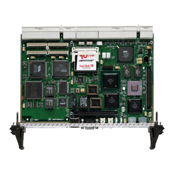
- Page 1 MCP750HA Hot Swap CompactPCI Single Board Computer Installation and Use MCP750HA/IH3 December 2000...
- Page 2 Motorola and the Motorola symbol are registered trademarks of Motorola, Inc. PowerPC™ is a trademark of IBM Corporation, and is used by Motorola, Inc. under license from IBM Corporation. CompactPCI is a registered trademark of PCI Industrial Computer Manufacturers Group.
- Page 3 The safety precautions listed below represent warnings of certain dangers of which Motorola is aware. You, as the user of the product, should follow these warnings and all other safety precautions necessary for the safe operation of the equipment in your operating environment.
- Page 4 Flammability All Motorola PWBs (printed wiring boards) are manufactured with a flammability rating of 94V-0 by UL-recognized manufacturers. EMI Caution This equipment generates, uses and can radiate electromagnetic energy. It may cause or be susceptible to electromagnetic interference (EMI) if not installed and used with adequate EMI protection.
- Page 5 While reasonable efforts have been made to assure the accuracy of this document, Motorola, Inc. assumes no liability resulting from any omissions in this document, or from the use of the information obtained therein. Motorola reserves the right to revise this document and to make changes from time to time in the content hereof without obligation of Motorola to notify any person of such revision or changes.
- Page 6 It is possible that this publication may contain reference to or information about Motorola products (machines and programs), programming, or services that are not available in your country. Such references or information must not be construed to mean that Motorola intends to announce such Motorola products, programming, or services in your country.
-
Page 7: Table Of Contents
Contents About This Manual Summary of Changes ....................xvii Overview of Contents ....................xviii Comments and Suggestions ..................xix Conventions Used in This Manual................xix CHAPTER 1 Hardware Preparation and Installation Introduction........................1-1 Equipment Required ....................1-3 Overview of Start-up Procedure ................1-4 Unpacking Instructions ....................1-5 Hardware Configuration ....................1-6 MCP750HA Base Board Preparation ................1-6 Flash Bank Selection (J9) ...................1-6 Hardware Installation..................1-9... - Page 8 DMA Channels....................2-7 Sources of Reset ....................2-7 Endian Issues ...................... 2-8 Processor/Memory Domain ................ 2-9 Role of the Raven ASIC................2-9 PCI Domain....................2-9 PCI and Ethernet ..................2-9 CHAPTER 3 Functional Description Introduction ....................... 3-1 Features........................3-1 General Description ....................3-2 Block Diagram......................
- Page 9 RESET(RST) Switch (S1) ................3-21 Reset and Abort Header (J21)................3-22 Front Panel Indicators (DS1 - DS4)..............3-22 Fuses and Polyswitches (Resettable Fuses) ............3-23 Speaker Control ....................3-23 MPC750 Processor ...................3-24 Flash Memory....................3-24 RAM300 Memory Module ................3-25 Compact FLASH Memory Card...............3-25 TMCP700 Transition Module................3-25 Serial Interface Modules................3-26 CHAPTER 4 Connector Pin Assignments...
- Page 10 Debugger System Call Interfaces ..............5-12 High Availability System Call Interfaces ..........5-12 Unsupported System Call Interfaces ............5-12 Bug Diagnostics....................... 5-13 Diagnostic Tests....................5-14 High Availability Diagnostic Commands ..........5-15 Unsupported PPCBug Diagnostic Commands.......... 5-16 CHAPTER 6 CNFG and ENV Commands Overview ........................
- Page 11 PMC I/O Connectors (J2/J21)................B-18 APPENDIX C Related Documentation Motorola Computer Group Documents ..............C-1 Manufacturers’ Documents..................C-2 Related Specifications....................C-3...
- Page 12 List of Figures Figure 1-1. MCP750HA Base Board Block Diagram..........1-2 Figure 1-2. MCP750HA Switches, Headers, Connectors, and LEDs......1-8 Figure 1-3. Compact FLASH Placement on MCP750HA........1-10 Figure 1-4. RAM300 Placement on MCP750HA............1-12 Figure 1-5. PMC Module Placement on MCP750HA ..........1-14 Figure 1-6. MCP750HA Board Insertion Sequence ..........1-17 Figure 2-1.
- Page 13 List of Tables Table 1-1. Startup Overview ..................1-4 Table 2-1. Processor Default View of the Memory Map ...........2-3 Table 2-2. PBC DMA Channel Assignments.............2-7 Table 2-3. Classes of Reset and Effectiveness ............2-8 Table 3-1. MCP750HA Features................3-1 Table 3-2. Series Termination for Ultra DMA EIDE..........3-13 Table 3-3.
- Page 14 Table B-8. Speaker Output Connector (J13) ............B-18 Table B-9. PMC I/O Connector (J2) ..............B-18 Table B-10. PMC I/O Connector (J21) ..............B-20 Table C-1. Motorola Computer Group Documents ..........C-1 Table C-2. Manufacturer’s Documents ..............C-2 Table C-3. Related Specifications ................C-3...
-
Page 15: Summary Of Changes
This manual provides general product information; hardware preparation, installation, and operating instructions along with a functional description of the MCP750HA series Single Board Computers (SBCs). These SBCs are used in conjunction with the Motorola CPX8000, CPX2000, and CPX1000 series systems. -
Page 16: Overview Of Contents
Overview of Contents This section outlines the contents of each chapter. Chapter 1, Hardware Preparation and Installation, outlines the hardware preparation and installation procedures for the MCP750HA series Single Board Computers. Chapter 2, Operating Instructions, provides information applicable to the MCP750HA family of Single Board Computers in a system configuration. -
Page 17: Comments And Suggestions
Comments and Suggestions Motorola welcomes and appreciates your comments on its documentation. We want to know what you think about our manuals and how we can make them better. Mail comments to: Motorola Computer Group Reader Comments DW164 2900 S. Diablo Way... - Page 18 <CR> represents the carriage return or Enter key. CTRL represents the Control key. Execute control characters by pressing the Ctrl key and the letter simultaneously, for example, Ctrl-d.
-
Page 19: Introduction
This manual provides general product information; hardware preparation, installation, and operating instructions along with a functional description of the MCP750HA series Single Board Computers (SBCs). These SBCs are used in conjunction with the Motorola CPX8000, CPX2000, and CPX1000 series systems. -
Page 20: Figure 1-1. Mcp750Ha Base Board Block Diagram
Hardware Preparation and Installation Flash/DRAM Expansion Debug Connector (8MB Linear Flash, up to 256MB of DRAM) FLASH Memory System Controller Registers L2 Cache Falcon Chipset Clock PCI Bridge Generator & MPIC Processor Raven ASIC MPC750 Reset Control Arbitration Control 33MHz 32/64-bit PCI Local Bus SROM AT24C04 Ethernet... -
Page 21: Equipment Required
One transition module supports all configurations of the board. Note Contact your local Motorola sales representative and/or your designated sales/systems engineer or distributor for the latest configuration specifications on the various MCP750HA models available. -
Page 22: Overview Of Start-Up Procedure
Hardware Preparation and Installation Overview of Start-up Procedure The following table lists the tasks that you will need to perform before using this board. It also informs you where to find the information you need to perform each step. Be sure to read this entire chapter (including all caution and warning notes) before you begin. -
Page 23: Unpacking Instructions
Unpack the equipment from the shipping carton. Carefully check the packing list and verify that all items are present. Save the packing material for storing and reshipping of equipment. Avoid touching areas of integrated circuitry; static discharge can damage circuits. Caution http://www.motorola.com/computer/literature... -
Page 24: Hardware Configuration
Hardware Preparation and Installation Hardware Configuration To produce the desired configuration and ensure proper operation of the MCP750HA, you may need to carry out certain hardware modifications before installing the module. The MCP750HA provides software control over most options: by setting bits in control registers after installing the module in a system, you can modify its configuration. - Page 25 Flash Bank B Enabled (1MB on base board) (8MB on RAM300 mezzanine) (Factory Configuration) J10 - Factory Use Only Header J10 is an ISP program download cable connection that is left on the board for MCG factory use only. http://www.motorola.com/computer/literature...
-
Page 26: Figure 1-2. Mcp750Ha Switches, Headers, Connectors, And Leds
Hardware Preparation and Installation CPCI Figure 1-2. MCP750HA Switches, Headers, Connectors, and LEDs Computer Group Literature Center Web Site... -
Page 27: Hardware Installation
ESD Precautions Use ESD Motorola strongly recommends that you use an antistatic wrist strap and a conductive foam pad when installing or upgrading a system. Electronic components such as disk drives, computer boards, and memory modules are extremely sensitive to ESD. -
Page 28: Figure 1-3. Compact Flash Placement On Mcp750Ha
Hardware Preparation and Installation secured to your wrist and to chassis ground throughout the procedure. 2. If you are installing the board in a non-hot swap chassis, perform an operating system shutdown. Turn the AC or DC power off and remove the AC cord or DC power lines from the system. -
Page 29: Ram300 Memory Mezzanine Installation
RAM300 Memory Mezzanine Installation The RAM300 DRAM mezzanine mounts on top of the MCP750HA base board. To upgrade or install a RAM300 mezzanine, refer to Figure 1-4 proceed as follows: http://www.motorola.com/computer/literature 1-11... -
Page 30: Figure 1-4. Ram300 Placement On Mcp750Ha
Hardware Preparation and Installation 1. Attach an ESD strap to your wrist. Attach the other end of the ESD strap to the chassis as a ground. The ESD strap must be secured to your wrist and to ground throughout the procedure. 2. -
Page 31: Pmc Module Installation
PMC Module Installation PCI mezzanine card (PMC) module mount beside the RAM300 mezzanine on top of the MCP750HA base board. To install a PMC module, refer to Figure 1-5 and proceed as follows: http://www.motorola.com/computer/literature 1-13... -
Page 32: Figure 1-5. Pmc Module Placement On Mcp750Ha
Hardware Preparation and Installation 1. Attach an ESD strap to your wrist. Attach the other end of the ESD strap to the chassis as a ground. The ESD strap must be secured to your wrist and to ground throughout the procedure. 2. -
Page 33: Mcp750Ha Module Installation
The ESD strap must be secured to your wrist and to ground throughout the procedure. 2. If the board is being installed in a non-hot swap chassis, perform an operating system shutdown. Turn the AC or DC power off and http://www.motorola.com/computer/literature 1-15... - Page 34 Hardware Preparation and Installation remove the AC cord or DC power lines from the system. Remove chassis or system cover(s) as necessary for access to the CompactPCI modules. To prevent injury, use extreme caution when handling, testing, and adjusting this equipment. Dangerous voltages capable of causing death exist.
-
Page 35: Figure 1-6. Mcp750Ha Board Insertion Sequence
6. Replace the chassis or system cover(s), making sure that no cables are pinched. Cable the peripherals to the panel connectors. For non- hot swap chassis, reconnect the system to the AC or DC power source, and turn the equipment power on. http://www.motorola.com/computer/literature 1-17... -
Page 36: System Considerations
Hardware Preparation and Installation System Considerations The MCP750HA is designed to operate as a CompactPCI system slot board. As a system slot board, the MCP750HA provides system clocks and arbitration for the other peripheral slots in the subrack. Consequently, the MCP750HA must be installed in a subrack system slot marked with a triangle symbol. -
Page 37: Introduction
2Operating Instructions Introduction This chapter provides information applicable to the MCP750HA family of Single Board Computers in a system configuration. This includes the power-up procedure along with descriptions of the switches and LEDs, memory maps, and software initialization. Applying Power After you have verified that all the necessary hardware preparation has been done (with all connections made correctly) and that the installation is complete, you can power up the system. -
Page 38: Memory Maps
Operating Instructions STARTUP SYSTEM INITIALIZATION CONSOLE DETECTION RUN SELF TESTS (IF ENABLED) AUTOBOOT (IF ENABLED) OPERATING SYSTEM 11734.00 9702 Figure 2-1. PPCBug System Startup The MCP750HA front panel has switches and four ABORT RESET LED status indicators ( ). For additional information on CPCI front panel operation, refer to Chapter 3, Functional... -
Page 39: Processor Memory Map
($00000000 to $FFFFFFFF). Table 2-1. Processor Default View of the Memory Map Processor Address Size Definition Notes Start 00000000 7FFFFFFF Not Mapped 80000000 8001FFFF 128KB PCI/ISA I/O Space 80020000 FEF7FFFF 2GB-16MB-640KB Not Mapped FEF80000 FEF8FFFF 64KB Falcon Registers http://www.motorola.com/computer/literature... -
Page 40: Pci Local Bus Memory Map
Operating Instructions Table 2-1. Processor Default View of the Memory Map (Continued) Processor Address Size Definition Notes Start FEF90000 FEFEFFFF 384KB Not Mapped FEFF0000 FEFFFFFF 64KB Raven Registers FF000000 FFEFFFFF 15MB Not Mapped FFF00000 FFFFFFFF ROM/Flash Bank A or Bank B Notes 1. -
Page 41: Compactpci Memory Map
There are 6 potential local PCI bus masters on the MCP750HA single- board computer: ❏ Raven ASIC (MPU/PCI bus bridge controller) ❏ DEC 21154 PCI-to-PCI bridge ❏ External PCI bus master via J4 connector, used by the hot swap bridge ❏ VIA 82C586B PBC (Peripheral Bus Controller) PCI/ISA bridge http://www.motorola.com/computer/literature... -
Page 42: Interrupt Handling
Operating Instructions ❏ DEC 21140 Ethernet Controller ❏ PMC Slot (PCI mezzanine card) The arbitration for these six bus mastering devices is provided by custom onboard hardware. This arbiter implements a rotating priority scheme in which the last master granted becomes the lowest priority. The order of rotation is shown in the list above. -
Page 43: Dma Channels
4. Watchdog timer Reset function controlled by the SGS-Thomson MK48T559 Watchdog Timer or the Raven Watchdog Timers. 5. Port 92 Register via the PBC 6. CompactPCI Bus via the 21154 Bridge Control Register. 7. Optional external reset from J5 pin A22. http://www.motorola.com/computer/literature... -
Page 44: Endian Issues
Operating Instructions Table 2-3 shows which devices are affected by the various types of resets. For details on using resets, refer to the MCP750 Single Board Computer Programmer's Reference Guide, listed in Appendix C, Related Documentation. Table 2-3. Classes of Reset and Effectiveness Device Processor Raven... -
Page 45: Processor/Memory Domain
Since the Raven maintains address invariance in both little-endian and big- endian mode, no endian issues should arise for Ethernet data. However, big-endian software must still take the byte-swapping effect into account when accessing the registers of the PCI/Ethernet device. http://www.motorola.com/computer/literature... -
Page 46: Introduction
3Functional Description Introduction This chapter describes the MCP750HA single-board computer on a block diagram level. The General Description on page 3-2 provides an overview of the MCP750HA, followed by a detailed description of several blocks of circuitry. Figure 3-1 shows a block diagram of the board’s architecture. Detailed descriptions of other MCP750HA blocks, including programmable registers in the ASICs and peripheral chips can be found in the MCP750 Single Board Computer Programmer’s Reference Guide,... -
Page 47: General Description
Functional Description Table 3-1. MCP750HA Features (Continued) Feature Description Interrupts Software interrupt handling via Raven (PCI-MPU bridge) and Peripheral Bus Controller Serial I/O 1 async port (COM1) via front panel. 2 async ports, 2 sync/async ports via the transition module Parallel I/O IEEE 1284 bidirectional parallel port (PC87307 SIO) via the transition module... - Page 48 Component Interconnect) bus. In addition to the on-board local bus peripherals, the PCI bus supports an industry-standard mezzanine interface, IEEE P1386.1 PMC (PCI Mezzanine Card). PMC modules offer a variety of possibilities for I/O expansion. The base board supports PMC I/O for the front panel or J3/TMCP700. http://www.motorola.com/computer/literature...
-
Page 49: Figure 3-1. Mcp750Ha Block Diagram
Functional Description Block Diagram Parallel L2 Cache MPC750 SRAM Keyboard Mouse Compact FLASH Async Serial (2 channels) 60X System Bus Sync/Async Serial ISA SIO (2 channels) Falcon IDE Bus DRAM Falcon ISA Local Resource Bus FLASH NVRAM Peripheral Bus ISA CSR Raven Controller Sys CSR... -
Page 50: Block Diagram
The arbiter parks the CPCI bus at the last bus master by keeping the last grant asserted until a new bus request is asserted. After a reset, the arbitter parks the CPCI bus at DEC21154 until a new request is asserted. http://www.motorola.com/computer/literature... -
Page 51: Pci Expansion Connector (J4)
Functional Description The MCP750HA provides the 33 MHz clocks for each of the CompactPCI slots. All clock source outputs are active when the MCP750HA is owner of the CPCI bus. The 21154 supports 3.3V or 5V signalling at the PCI busses with a separate VIO pin for the primary and secondary bus buffers. -
Page 52: Domain Ownership
The backplane must leave the control lines J3-A15, J3-A16, J3-A17, and J3-A18 as no connects in non- high availability implementations. Pull-up resistors located on the MCP750HA will then allow for normal PCI-to-PCI Bridge operation. http://www.motorola.com/computer/literature... -
Page 53: Ethernet Interface
Functional Description In the high availability systems, a Hot Swap Controller device is present on the local PCI bus. This device can be used by the software to gain or relinquish control of the Domains (CPCI buses). The HSC is also used to oversee the HA functionality of the other I/O boards inserted into the non- host system slots. -
Page 54: Pci Mezzanine Interface
IEEE P1386.1 PCI Mezzanine Card (PMC). PMC modules offer a variety of possibilities for I/O expansion through Fiber Distributed Data Interface (FDDI), Asynchronous Transfer Mode (ATM), graphics, and Ethernet ports. The base board supports PMC front panel and rear transition module I/O. http://www.motorola.com/computer/literature... -
Page 55: Pc97307 Isa Super I/O Device
Functional Description The MCP750HA supports one PMC slot. Four 64-pin connectors on the base board (J11, J12, J13, and J14) interface with 32-bit or 64-bit IEEE P1386.1 PMC-compatible mezzanines to add any desirable function. The PCI Mezzanine Card slot has the following characteristics: Mezzanine Type PMC (PCI Mezzanine Card) Mezzanine Size... -
Page 56: Parallel Port/Printer Interface
Software written for those devices may be used without change to operate the ISA Super I/O controller. The ISA Super I/O device may be used to support any of the following devices: ❏ -inch 1.44MB floppy disk drive http://www.motorola.com/computer/literature 3-11... -
Page 57: Keyboard And Mouse Interface
To get both keyboard and mouse functions requires a Y adapter cable (Motorola Part Number: 30NW9302B83). Refer to the TMCP700 Transition Module Installation and Use manual for details. -
Page 58: Eide Series Termination
82 ohm RESET# 33 ohm Real-Time Clock/NVRAM/Watchdog Timer Function The MCP750HA employs an ST Microelectronics surface-mount M48T559 RAM and clock chip to provide 8KB of non-volatile static RAM, a real-time clock, and a watchdog timer function. This chip supplies http://www.motorola.com/computer/literature 3-13... -
Page 59: Programmable Timers
Functional Description a clock, oscillator, crystal, power failure detection, memory write protection, 8KB of NVRAM, and a battery in a package consisting of two parts: ❏ A 28-pin 330mil SO device containing the real-time clock, the oscillator, power failure detection circuitry, timer logic, 8KB of static RAM, and gold-plated sockets for a battery ❏... -
Page 60: Raven Watchdog Timers
The PBC has three built-in counters that are equivalent to those found in an 82C54 programmable interval timer. The counters are grouped into one timer unit, Timer 1, in the PBC. Each counter output has a specific function: http://www.motorola.com/computer/literature 3-15... -
Page 61: 16-Bit Timers
Functional Description ❏ Counter 0 is associated with interrupt request line IRQ0. It can be used for system timing functions, such as a timer interrupt for a time-of-day function. ❏ Counter 1 generates a refresh request signal for ISA memory. This timer is not used in the MCP750HA. -
Page 62: Z8536 Cio Device
The CPU Configuration Register is an 8-bit register located at ISA I/O address x0800. The CPUType field will return Eh for the MCP750HA. Table 3-3. Old CPU Configuration Register Old CPU Configuration Register - $FE000800 FIELD CPUTYPE OPER RESET http://www.motorola.com/computer/literature 3-17... -
Page 63: Base Module Feature Register
Functional Description ❏ The Base Module Status Register is an 8-bit read-only register located at ISA I/O address x803. The BASE_TYPE field will return E2h for the MCP750HA. Table 3-4. Base Module Status Register Base Module Status Register - Offset $0803 FIELD BASE_TYPE OPER... -
Page 64: Serial Port Signal Multiplexing
MXDO, and MXDI. MXCLK is the 10 MHz bit clock for the time-multiplexed data lines MXDO and MXDI. MXSYNC# is asserted for one bit time at Time Slot 15 by the MCP750HA board. MXSYNC# is used by the transition http://www.motorola.com/computer/literature 3-19... -
Page 65: Table 3-5. Multiplexing Sequence Of The Mx Function
Functional Description module to synchronize with the MCP750HA board. MXDO is the time- multiplexed output line from the main board and MXDI is the time- multiplexed line from the transition module. A 16-to-1 multiplexing scheme is used with 10 MHz bit rate. Sixteen Time Slots are defined and allocated as follows: Table 3-5. -
Page 66: Abort(Abt) Switch (S2)
PB7 of the Z8536 CIO device, which handles various status signals, serial I/O lines, and counters. The interrupter connected to the switch is an edge-sensitive circuit, ABORT filtered to remove switch bounce. RESET(RST) Switch (S1) switch resets all onboard devices and generates a CompactPCI RESET backplane reset. http://www.motorola.com/computer/literature 3-21... -
Page 67: Reset And Abort Header (J21)
Functional Description Reset and Abort Header (J21) A three pin header is provided to facilitate remote reset and abort operations. Connection to J21 will allow external stimulation of the Reset and Abort signal lines just as if the front panel switches were depressed. Refer to Chapter 4, Connector Pin Assignments, for the definition of pin... -
Page 68: Fuses And Polyswitches (Resettable Fuses)
The MCP750HA base board supplies a signal to the SPEAKER_OUT transition module. The transition module contains a two pin jumper header (J13) which allows the signal to be cabled to an external SPEAKER_OUT speaker to obtain a beep tone. http://www.motorola.com/computer/literature 3-23... -
Page 69: Mpc750 Processor
Functional Description MPC750 Processor The MCP750HA is designed to support the enhanced version of the MPC750 360-pin BGA processor chip with 32MB to 256MB of ECC DRAM, 1MB of level 2 cache (L2 cache), and up to 9MB of Flash memory. -
Page 70: Ram300 Memory Module
Once configured, this memory will appear as a standard ATA (EIDE) disk drive. TMCP700 Transition Module The TMCP700 transition module (see Appendix B, Hardware Preparation and Installation for TMCP700, for more information) is used in conjunction with all models of the MCP750HA base board. http://www.motorola.com/computer/literature 3-25... -
Page 71: Serial Interface Modules
Functional Description The features of the TMCP700 include: ❏ A parallel printer port (IEEE 1284-I compliant) ❏ Two EIA-232-D asynchronous serial ports (identified as COM1 on the front panel) COM2 ❏ Two synchronous serial ports ( on the front SERIAL 3 SERIAL 4 panel), configured for EIA-232-D, EIA-530, V.35, or X.21 protocols... - Page 72 Module Type SIMV35DCE V.35 DCE SIMV35DTE V.35 DTE SIMX21DCE X.21 DCE SIMX21DTE X.21 DTE For additional information about the serial interface modules, refer to the TMCP700 Transition Module Installation and Use manual, listed in Appendix C, Related Documentation. http://www.motorola.com/computer/literature 3-27...
-
Page 73: Mcp750Ha Connectors
4Connector Pin Assignments MCP750HA Connectors This chapter summarizes the pin assignments for the following groups of connectors and headers for the MCP750HA: ❏ CompactPCI Connectors (J1/J2) ❏ CompactPCI HSC/User I/O Connector (J3) ❏ Local Bus Expansion Connector (J4) ❏ User I/O Connector (J5) ❏... -
Page 74: Compactpci Connectors (J1/J2)
Connector Pin Assignments CompactPCI Connectors (J1/J2) The MCP750HA implements a 64-bit CompactPCI interface on connectors J1 and J2. J1 is a 110 pin AMP Z-pack 2mm hard metric type A connector with keying for +3.3V or +5V. J2 is a 110 pin AMP Z-pack 2mm hard metric type B connector. -
Page 75: Table 4-2. Compactpci Connector J2
No Connect PRST_L REQ6_L GNT6_L (BRSVP2A17) No Connect No Connect DEG_L No Connect (BRSVP2A16) (BRSVP2B16) (BRSVP2E16) No Connect FAL_L REQ5_L GNT5_L (BRSVP2A15) AD35 AD34 AD33 AD32 AD38 AD37 AD36 AD42 AD41 AD40 AD39 AD45 AD44 AD43 AD49 AD48 AD47 AD46 http://www.motorola.com/computer/literature... -
Page 76: Compactpci Hsc/User I/O Connector (J3)
Connector Pin Assignments Table 4-2. CompactPCI Connector J2 (Continued) AD52 AD51 AD50 AD56 AD55 AD54 AD53 AD59 AD58 AD57 AD63 AD62 AD61 AD60 CBE5_L CBE4_L PAR64 No Connect CBE7_L CBE6_L (BRSVP2B4) CLK4 GNT3_L REQ4_L GNT4_L CLK2 CLK3 SYSEN_L GNT2_L REQ3_L CLK1 REQ1_L GNT1_L... -
Page 77: Local Bus Expansion Connector (J4)
AD37 AD45 AD44 AD43 AD42 AD41 AD49 3.3V AD48 AD47 AD46 AD53 AD52 AD51 AD50 AD57 3.3V AD56 AD55 AD54 AD61 AD60 AD59 AD58 CBE4# 3.3V PAR64 AD63 AD62 REQ64# CBE7# CBE6# CBE5# 3.3V ACK64# 12-14 KEY AREA 12-14 http://www.motorola.com/computer/literature... -
Page 78: Table 4-5. J5 User I/O Connector
Connector Pin Assignments Table 4-4. J4 Local PCI Expansion Connector (Continued) CBE0# AD13 5.0V AD12 AD11 AD10 CBE1# AD15 AD14 STOP# 5.0V LOCK# PERR# SERR# FRAME# IRDY# TRDY# DEVSEL# AD18 5.0V AD17 AD16 CBE2# AD21 AD20 AD19 CBE3# 5.0V No Connect AD23 AD22 AD28... -
Page 79: Table 4-6. Pci Mezzanine Card Connector
(PMC). The pin assignments are listed in the following two tables: Table 4-6. PCI Mezzanine Card Connector ∗ –12V +12V TRST ∗ PMCINTA ∗ ∗ PMCINTB PMCINTC ∗ PMC1P Not Used ∗ PMCINTD Not Used Not Used Not Used Not Used Pull-up +3.3V ∗ PCICLK PCIRST Pull-down http://www.motorola.com/computer/literature... - Page 80 Connector Pin Assignments Table 4-6. PCI Mezzanine Card Connector (Continued) ∗ PMC1GNT +3.3V Pull-down ∗ PMC1REQ Not Used AD31 AD30 AD29 AD28 AD27 AD26 AD25 AD24 +3.3V ∗ CBE3 IDSEL AD23 AD22 AD21 +3.3V AD20 AD19 AD18 ∗ AD17 AD16 C/BE2 ∗...
-
Page 81: Table 4-7. Pci Mezzanine Card Connector
AD47 AD46 PMCIO35 PMCIO36 AD45 PMCIO37 PMCIO38 +5V (Vio) AD44 PMCIO39 PMCIO40 AD43 AD42 PMCIO41 PMCIO42 AD41 PMCIO43 PMCIO44 AD40 PMCIO45 PMCIO46 AD39 AD38 PMCIO47 PMCIO48 AD37 PMCIO49 PMCIO50 AD36 PMCIO51 PMCIO52 AD35 AD34 PMCIO53 PMCIO54 AD33 PMCIO55 PMCIO56 http://www.motorola.com/computer/literature... -
Page 82: Front Usb Connectors (J17/J18)
Connector Pin Assignments Table 4-7. PCI Mezzanine Card Connector +5V (Vio) AD32 PMCIO57 PMCIO58 Not Used Not Used PMCIO59 PMCIO60 Not Used PMCIO61 PMCIO62 Not Used PMCIO63 PMCIO64 Front USB Connectors (J17/J18) Two USB Series A receptacles are located at the front panel of the MCP750HA SBC. -
Page 83: Com1 Connector (J15)
J11 on the transition module. A terminal may be connected to J15 or J11 on the transition module but not both at the same time. The pin assignments for this connector is as follows: Table 4-11. COM1 Connector J15 http://www.motorola.com/computer/literature 4-11... -
Page 84: Reset And Abort Header (J21)
Connector Pin Assignments Reset and Abort Header (J21) A three-pin header is provided to facilitate remote reset and abort operations. Connection to J21 will allow external stimulation of the Reset and Abort signal lines just as if the front panel switches were depressed. The reset and abort signal lines must be asserted for a minimum time period of 10 microseconds to assure the input will take effect. - Page 85 ∗ RSRV PD10 PD11 PD12 PD13 PD14 PD15 PD16 PD17 PD18 PD19 PA20 PD21 PD22 PD23 PD24 PD25 PD26 PD27 PD28 PD29 PD30 PD31 PD32 PD33 PD34 PD35 PD36 PD37 PD38 PD39 PD40 PD41 PD42 PD43 PD44 PD45 http://www.motorola.com/computer/literature 4-13...
- Page 86 Connector Pin Assignments Table 4-13. Debug Connector (J16) (Continued) PD46 PD47 PD48 PD49 PA50 PD51 PD52 PD53 PD54 PD55 PD56 PD57 PD58 PD59 PD60 PD61 PD62 PD63 PDPAR0 PDPAR1 PDPAR2 PDPAR3 PDPAR4 PDPAR5 PDPAR6 PDPAR7 No Connection No Connection ∗ ∗...
- Page 87 No Connection No Connection ∗ No Connection No Connection ∗ No Connection No Connection No Connection NAPRUN ∗ ∗ SRST1 QREQ ∗ ∗ SRESET QACK ∗ HRESET CPUTDO CPUTDI CPUCLK1 CPUTCK No Connection CPUTMS ∗ No Connection CPUTRST http://www.motorola.com/computer/literature 4-15...
-
Page 88: Dram Mezzanine Connector (J7)
Connector Pin Assignments DRAM Mezzanine Connector (J7) A 190-pin connector (J7 on the MCP750HA base board) supplies the interface between the memory bus and the RAM300 DRAM mezzanine. The pin assignments are listed in the following table. Table 4-14. DRAM Mezzanine Connector (J7) ∗... - Page 89 RDL28 RDL29 RDL30 RDL31 RDL32 RDL33 RDL34 RDL35 RDL36 RDL37 RDL38 RDL39 RDL40 RDL41 RDL42 RDL43 RDL44 RDL45 RDL46 RDL47 RDL48 RDL49 RDL50 RDL51 RDL52 RDL53 RDL54 RDL55 RDL56 RDL57 RDL58 RDL59 RDL60 RDL61 RDL62 RDL63 CDL0 CDL1 http://www.motorola.com/computer/literature 4-17...
- Page 90 Connector Pin Assignments Table 4-14. DRAM Mezzanine Connector (J7) (Continued) CDL2 CDL3 CDL4 CDL5 CDL6 CDL7 No Connection No Connection RDU0 RDU1 RDU2 RDU3 RDU4 RDU5 RDU6 RDU7 RDU8 RDU9 RDU10 RDU11 RDU12 RDU13 RDU14 +3.3V RDU15 RDU16 RDU17 RDU18 RDU19 RDU20 RDU21...
-
Page 91: Eide Compact Flash Connector (J20)
A 50-pin Compact FLASH card header connector provides the EIDE interface to the Compact FLASH Memory Card. The pin assignments for this connector are as follows: Table 4-15. EIDE Compact FLASH Connector J20 DATA3 DATA4 DATA5 DATA6 DATA7 DCS1A_L http://www.motorola.com/computer/literature 4-19... - Page 92 Connector Pin Assignments Table 4-15. EIDE Compact FLASH Connector J20 (Continued) DATA0 DATA1 DATA2 NO CONNECT CD2_L CD1_L DATA11 DATA12 DATA13 DATA14 DATA15 DCS3A_L NO CONNECT DIORA_L DIOWA_L NO CONNECT INTRQA MASTER/SLAVE NO CONNECT RST_L DIORDYA NO CONNECT NO CONNECT NO CONNECT NO CONNECT DATA8...
-
Page 93: Ppcbug Overview
Documentation. PPCBug Basics The PowerPC debug firmware (PPCBug) is a powerful evaluation and debugging tool for systems built around the Motorola PowerPC microcomputers. Facilities are available for loading and executing user programs under complete operator control for system evaluation. The PPCBug provides a high degree of functionality, user friendliness, portability, and ease of maintenance. - Page 94 PPCBug ❏ Display and modification of memory ❏ Breakpoint and tracing capabilities ❏ A powerful assembler and disassembler useful for patching programs ❏ A self-test at power-up feature which verifies the integrity of the system The PPCBug consists of three parts: ❏...
-
Page 95: Memory Requirements
This process occurs each time the MCP750HA is reset or powered up. The steps below represent high-level outline (not all of the detailed steps are listed): 1. Sets MPU.MSR to known value. 2. Invalidates the MPU's data/instruction caches. 3. Clears all segment registers of the MPU. http://www.motorola.com/computer/literature... - Page 96 PPCBug 4. Clears all block address translation registers of the MPU. 5. Initializes the MPU-bus-to-PCI-bus bridge device. 6. Initializes the PCI-bus-to-ISA-bus bridge device. 7. Calculate the external bus clock speed of the MPU. 8. Delays for 750 milliseconds. 9. Determines the CPU board type. 10.
- Page 97 35. Executes Self-Test, if so configured. (Default is no Self-Test.) 36. Extinguishes the board fail LED, if there are no self-test failures or initialization/configuration errors. 37. Executes the configured boot routine, either ROMboot, Autoboot, or Network Autoboot. 38. Executes the user interface (displays the <PPC1(A)-Bug> prompt). <PPC1(A)-Diag> http://www.motorola.com/computer/literature...
-
Page 98: Using Ppcbug
PPCBug Using PPCBug PPCBug is command-driven; it performs its various operations in response to commands that you enter at the keyboard. When the <PPC1(A)-Bug> prompt appears on the screen, the debugger is ready to accept debugger commands. When the prompt appears on the screen, the PPC1(A)-Diag>... -
Page 99: Debugger Commands
HE, followed by a space, followed by the test category description (for example, UART), followed by a carriage return Table 5-1. Debugger Commands Command Description One Line Assembler Block of Memory Compare Block of Memory Fill Block of Memory Initialize Block of Memory Move http://www.motorola.com/computer/literature... - Page 100 PPCBug Table 5-1. Debugger Commands (Continued) Command Description Breakpoint Insert NOBR Breakpoint Delete Block of Memory Search Block of Memory Verify Concurrent Mode NOCM No Concurrent Mode CNFG Configure Board Information Block Checksum CSAR PCI Configuration Space READ Access CSAW PCI Configuration Space WRITE Access Data Conversion One Line Disassembler...
- Page 101 Network Boot Operating System NIOC Network I/O Control NIOP Network I/O Physical NIOT Network I/O Teach (Configuration) NPING Network Ping Offset Registers Display/Modify Printer Attach NOPA Printer Detach PBOOT Bootstrap Operating System Port Format NOPF Port Detach PFLASH Program FLASH Memory http://www.motorola.com/computer/literature...
- Page 102 PPCBug Table 5-1. Debugger Commands (Continued) Command Description Put RTC into Power Save Mode ROMboot Enable NORB ROMboot Disable Register Display REMOTE Remote RESET Cold/Warm Reset Read Loop Register Modify Register Set Switch Directories Set Time and Date SROM SROM Examine/Modify Symbol Table Attach NOSYM Symbol Table Detach...
-
Page 103: High Availability Commands
The following table lists PPCBug debugger commands that have been added to support High Availability (HA) features. These are only available when the MCP750HA is used in a system with the appropriate Motorola Hot Swap Controller. Table 5-2. High Availability Specific Debugger Commands... -
Page 104: Debugger System Call Interfaces
PPCBug Table 5-3. Unsupported Debugger Commands (Continued) Name Description Idle MPU Register Modify Idle MPU Register Set Nap MPU MPU Execution/Status Debugger System Call Interfaces High Availability System Call Interfaces The following table lists debugger system call interfaces that have been added to support High Availability (HA) functionality. -
Page 105: Bug Diagnostics
Availability (HA) features of the CPU module. It includes tests for: ❏ Memory Read/Write ❏ L2 Cache ❏ Real Time Clock ❏ Ethernet Controller ❏ ISA Bridge ❏ Serial Communications Controller ❏ UART ❏ Keyboard/Mouse Controller ❏ Parallel Interface ❏ PCI/PMC Interface ❏ EIDE ❏ Counter/Timer http://www.motorola.com/computer/literature 5-13... -
Page 106: Diagnostic Tests
PPCBug Diagnostic Tests In order to use the diagnostics, you must switch to the diagnostic directory. You may switch between directories by using the SD (Switch Directories) command. You may view a list of the commands in the directory that you are currently in by using the HE (Help) command. -
Page 107: High Availability Diagnostic Commands
Availability PPCBug Firmware User’s Manual, listed in Appendix C, Related Documentation. Table 5-7. PPCBug Diagnostic Commands For High Availability Systems Name Description Abbreviated Self-Tests Hot Swap Controller/Bridge Tests (requires Hot Swap Controller) IFC4526 Interphase Fibre Channel Tests (requires Interphase Fibre Channel PMC) http://www.motorola.com/computer/literature 5-15... -
Page 108: Unsupported Ppcbug Diagnostic Commands
PPCBug Unsupported PPCBug Diagnostic Commands The following table lists PPCBug diagnostic commands that are part of the standard PPCBug package, but are not supported on the MCP750HA system. Table 5-8. Unsupported PPCBug Diagnostic Commands Name Description CL1283 Parallel Interface (Cirrus CL-CD1283) Tests CS4231 CS4231 Audio Codec Tests VGA543X... -
Page 109: Overview
6CNFG and ENV Commands Overview You can use the factory-installed debug monitor, PPCBug, to modify certain parameters contained in the PowerPC board's Non-Volatile RAM (NVRAM), also known as Battery Backed-up RAM (BBRAM). ❏ The Board Information Block in NVRAM contains various elements concerning operating parameters of the hardware. -
Page 110: Env - Set Environment
Local SCSI Identifier* = “07 ” System Serial Number = “1234567 ” System Identifier = “Motorola MCP750603-001a ” License Identifier 12345678 ” “ The value or identifier to the left of the equal sign is displayed as left- justified character (ASCII) strings padded with space characters and quotes (“) are displayed to indicate the size of the string. -
Page 111: Configuring The Ppcbug Parameters
Auto-Initialize of NVRAM Header Enable [Y/N] = Y? NVRAM (PReP partition) header space will be initialized automatically during board initialization, but only if the PReP partition fails a sanity check (Default). NVRAM header space will not be initialized automatically during board initialization. http://www.motorola.com/computer/literature... - Page 112 CNFG and ENV Commands Network PReP-Boot Mode Enable [Y/N] = N? Enable PReP-style network booting (same boot image from a network interface as from a mass storage device). Do not enable PReP-style network booting (Default). SCSI Bus Reset on Debugger Startup [Y/N] = N? SCSI bus is reset on debugger setup.
- Page 113 If Autoboot is enabled, the Autoboot process attempts to boot from devices specified in the scan list (e.g., ) (Default). FDISK/CDROM/TAPE/HDISK If Autoboot is enabled, the Autoboot process uses the Controller LUN and Device LUN to boot. Auto Boot Scan Device Type List = FDISK/CDROM/TAPE/HDISK? http://www.motorola.com/computer/literature...
- Page 114 CNFG and ENV Commands This is the listing of boot devices displayed if the Autoboot Scan option is enabled. If you modify the list, follow the format shown above (uppercase letters, using forward slash as separator). Auto Boot Controller LUN = 00? Refer to the PPCBug Firmware Package User's Manual, listed in Appendix C, Related...
- Page 115 NETboot is attempted at any reset (Default). Network Auto Boot Controller LUN = 00? Refer to the PPCBug Firmware Package User's Manual, listed in Appendix C, Related Documentation, for a listing of network controller modules currently supported by PPCBug (Default = $00). http://www.motorola.com/computer/literature...
- Page 116 CNFG and ENV Commands Network Auto Boot Device LUN = 00? Refer to the PPCBug Firmware Package User's Manual, listed in Appendix C, Related Documentation, for a listing of network controller modules currently supported by PPCBug (Default = $00). Network Auto Boot Abort Delay = 5? The time in seconds that the NETboot sequence will delay before starting the boot.
- Page 117 (Memory Control Configuration Register 8: bits 23-27) to indicate the number of clock cycles used in accessing the ROM. The lowest allowable ROMFAL setting is $00; the highest allowable is $1F. The value to enter depends on processor speed; refer to your http://www.motorola.com/computer/literature...
- Page 118 CNFG and ENV Commands Processor/Memory Mezzanine Module User’s Manual, listed in Appendix C, Related Documentation, for appropriate values. The default value varies according to the system’s bus clock speed. Note ROM First Access Length is not applicable to the MCP750. The configured value is ignored by PPCBug.
- Page 119 A will be made. In a dual host processor system, if domain A is owned by the other host processor, no attempt will be made to claim the domain or power on slots. (Default = N) http://www.motorola.com/computer/literature 6-11...
- Page 120 CNFG and ENV Commands Domain A will be claimed during board power-up and board reset. The domain will only be claimed if the other processor board does not already own this domain. A non-system slot will not be powered on unless its bit is asserted in the slot power control word.
- Page 121 Firmware Command Buffer Enable [Y/N] = N? This parameter controls whether or not the processor will execute the Firmware Command Buffer during the boot process. (Default = N) Enable the command buffer during board power-up or board reset. Command buffer is disabled (Default) http://www.motorola.com/computer/literature 6-13...
- Page 122 CNFG and ENV Commands Firmware Command Buffer Delay = 5? The time, in seconds, that the firmware command buffer execution sequence will delay before starting. The purpose of the delay is to allow the user the option of stopping the execution by use of the BREAK key.
-
Page 123: Appendix A Specifications
ASpecifications Specifications Table A-1 lists the general specifications for MCP750HA base boards. Subsequent sections detail cooling requirements and FCC compliance. A complete functional description of the MCP750HA base boards appears Chapter 3, Functional Description. Specifications for the optional PCI mezzanines can be found in the documentation for those modules. Table A-1. -
Page 124: Cooling Requirements
Specifications Cooling Requirements The Motorola MCP750 (including the MCP750HA and CPX750HA) family of Single Board Computers is specified, designed, and tested to operate reliably with an incoming air temperature range from -5° to +55° C (32° to 131° F) with forced air cooling of the entire assembly (base board and modules) at a velocity typically achievable by using a 100 CFM axial fan. - Page 125 ❏ Front panel screws properly tightened. For minimum RF emissions, it is essential that the conditions above be implemented. Failure to do so could compromise the EMC compliance of the equipment containing the module. http://www.motorola.com/computer/literature...
-
Page 126: Introduction
Pin Assignment information for the TMCP700 Transition Module. The TMCP700 is an optional module that is used in conjunction with the MCP750HA series of Single Board Computers. If you are using the TMCP700 with the MCP750HA, ensure that you have... - Page 127 Hardware Preparation and Installation for TMCP700 The features of the TMCP700 include: ❏ A parallel printer port (IEEE 1284-I compliant) ❏ Two EIA-232-D asynchronous serial ports (identified as COM1 on the transition module’s panel) COM2 ❏ Two synchronous serial ports (identified as SERIAL 3 SERIAL 4 on the transition module’s panel), configured for EIA-232-D, EIA-...
- Page 128 TMCP700 Transition Module Preparation Figure B-1. TMCP700 Connector and Header Locations http://www.motorola.com/computer/literature...
-
Page 129: Serial Ports 1 And 2
Hardware Preparation and Installation for TMCP700 Serial Ports 1 and 2 The asynchronous serial ports (Serial Ports 1 and 2) are configured permanently as data circuit-terminating equipment (DTE). The port configuration is shown in Figure B-2. The port is also routed to a COM1 DB9 connector on the front panel of the processor board. - Page 130 TMCP700 Transition Module Installation and Use guide, listed in Appendix C, Related Documentation. The next three figures illustrate the MCP750HA base board and TMCP700 transition module with the interconnections and jumper settings for DCE/DTE configuration on each serial port. http://www.motorola.com/computer/literature...
- Page 131 Hardware Preparation and Installation for TMCP700 MCP750HA COM1 (Front Panel DB9) TMCP700 SOUT1 RTS1# DTR1# SIN1 CTS1# COM1 DSR1# DCD1# RI1# PC87307 SOUT2 RTS2# DTR2# SIN2 CTS2# COM2 DSR2# DCD2 RI2# 2098 9710 Figure B-2. MCP750HA/TMCP700 Serial Ports 1 and 2 (DTE Only) Computer Group Literature Center Web Site...
- Page 132 TMCP700 Transition Module Preparation MCP750HA TMCP700 Z85230 SCC EIA232-DTE SIM RTS# CTS# DCD# J8/J9 TRXC RTXC J3/MX Z8536 CIO DTR# LLB# RLB# DSR# 2097 9709 Figure B-3. TMCP700 Serial Ports 3 and 4 DCE Configuration http://www.motorola.com/computer/literature...
- Page 133 Hardware Preparation and Installation for TMCP700 MCP750HA TMCP700 Z85230 SCC EIA232-DTE SIM RTS# CTS# DCD# J8/J9 TRXC RTXC J3/MX Z8536 CIO DTR# LLB# RLB# DSR# 2096 9709 Figure B-4. TMCP700 Serial Ports 3 and 4 DTE Configuration Computer Group Literature Center Web Site...
-
Page 134: Esd Precautions
TMCP700 Transition Module Installation ESD Precautions Motorola strongly recommends that you use an antistatic wrist strap and a Use ESD conductive foam pad when installing or upgrading a system. Electronic components such as disk drives, computer boards, and memory modules are extremely sensitive to ESD. - Page 135 Hardware Preparation and Installation for TMCP700 Even in a hot swap capable chassis, the MCP750HA back end power should be switched off (or the chassis power shut down) prior to inserting or removing its corresponding transition module. To prevent injury, use extreme caution when handling, testing, and adjusting this equipment.
-
Page 136: Tmcp700 Transition Module
TMCP700 Transition Module MCP750 TMCP700 Figure B-5. TMCP700/MCP750HA Mating Configuration TMCP700 Transition Module The following tables summarize the pin assignments of connectors that are specific to MCP750HA modules configured for use with TMCP700 transition modules. http://www.motorola.com/computer/literature B-11... -
Page 137: Compactpci Connectors (J3/J4/J5
Hardware Preparation and Installation for TMCP700 CompactPCI Connectors (J3/J4/J5) Connector J3 is a 95-pin 2mm hard metric type B connector which routes I/O signals for PMC I/O and serial channels. The pinout for this connector has been described previously in Table 4-1 on page 4-2. -
Page 138: Serial Ports 3 And 4 (J6/J24) (Tmcp700 I/O Mode
Table B-2. Serial Connections - Ports 3 and 4 (J6 and J24) (TMCP700) No Connection TXDn RXDn RTSn CTSn DSRn DCDn SPn_P9 SPn_P10 SPn_P11 SPn_P12 SPn_P13 SPn_P14 TXCIn SPn_P16 RXCIn LLBn SPn_P19 DTRn RLBn http://www.motorola.com/computer/literature B-13... -
Page 139: Parallel Connector (J7) (Tmcp700 I/O Mode
Hardware Preparation and Installation for TMCP700 Table B-2. Serial Connections - Ports 3 and 4 (J6 and J24) (TMCP700) (Continued) SPn_P23 TXCOn SPn-P26 Parallel Connector (J7) (TMCP700 I/O Mode) The parallel interface is implemented with an IEEE P1284 36-pin connector (J7) located on the TMCP700 transition module. The pin assignments are listed in the following table. -
Page 140: Keyboard/Mouse Connector (J16) (Tmcp700 I/O Mode
MCP750HA front panel USB connections. An alternate build option of the MCP750HA may route the USB signals to the TMCP700 Transition Module in place of the MCP750HA front panel connectors. http://www.motorola.com/computer/literature B-15... -
Page 141: Eide Connector (J15
Hardware Preparation and Installation for TMCP700 EIDE Connector (J15) The TMCP700 provides a 40-pin header (J15) to interface to the MCP750HA secondary EIDE port. The pin assignments and signal mnemonics for this connector are listed in the following table: Table B-5. EIDE Connector (J15) Signal Signal DRESET_L... -
Page 142: Floppy Port Connector (J17
This power is derived from the fused +5VDC power on the MCP750HA. Any external device powered from this connector must not draw more than 200mA. The pin assignments are listed in the following table. http://www.motorola.com/computer/literature B-17... -
Page 143: Speaker Output Connector (J13
Hardware Preparation and Installation for TMCP700 Table B-7. +5Vdc Power Connector (J14) Signal +5Vdc No Connect Speaker Output Connector (J13) The 2-pin header (J13) provides connection to an external speaker from the MCP750HA PCB Counter 2 output. The pin assignments are listed in the following table. - Page 144 TMCP700 Transition Module Table B-9. PMC I/O Connector (J2) (Continued) Signal Signal PMCIO5 PMCIO6 PMCIO7 PMCIO8 PMCIO9 PMCIO10 PMCIO11 PMCIO12 PMCIO13 PMCIO14 PMCIO15 PMCIO16 PMCIO17 PMCIO18 PMCIO19 PMCIO20 PMCIO21 PMCIO22 PMCIO23 PMCIO24 PMCIO25 PMCIO26 PMCIO27 PMCIO28 PMCIO29 PMCIO30 PMCIO31 PMCIO32 http://www.motorola.com/computer/literature B-19...
-
Page 145: Table B-10. Pmc I/O Connector (J21
Hardware Preparation and Installation for TMCP700 Table B-10. PMC I/O Connector (J21) Signal Signal PMCIO33 PMCIO34 PMCIO35 PMCIO36 PMCIO37 PMCIO38 PMCIO39 PMCIO40 PMCIO41 PMCIO42 PMCIO43 PMCIO44 PMCIO45 PMCIO46 PMCIO47 PMCIO48 PMCIO49 PMCIO50 PMCIO51 PMCIO52 PMCIO53 PMCIO54 PMCIO55 PMCIO56 PMCIO57 PMCIO58 PMCIO59 PMCIO60 B-20... - Page 146 TMCP700 Transition Module Table B-10. PMC I/O Connector (J21) (Continued) Signal Signal PMCIO61 PMCIO62 PMCIO63 PMCIO64 http://www.motorola.com/computer/literature B-21...
-
Page 147: Motorola Computer Group Documents
CRelated Documentation Motorola Computer Group Documents The Motorola publications listed below are referenced in this manual. You can obtain paper or electronic copies of Motorola Computer Group publications by: ❏ Contacting your local Motorola sales office ❏ Visiting Motorola Computer Group’s World Wide Web literature site, http://www.motorola.com/computer/literature... -
Page 148: Manufacturers' Documents
Table C-2. Manufacturer’s Documents Document Title and Source Publication Number MCP750 RISC Microprocessor Technical Summary MPC750/D Literature Distribution Center for Motorola Telephone: 1-800- 441-2447 FAX: (602) 994-6430 or (303) 675-2150 http://merchant.hibbertco.com/mtrlext/ E-mail: ldcformotorola@hibbertco.com LTC1643L/LTC1643H Data Sheet LTC1643L/... -
Page 149: Related Specifications
As an additional help, a source for the listed document is also provided. Please note that, while these sources have been verified, the information is subject to change without notice. Table C-3. Related Specifications Document Title and Source Publication Number IEEE - Common Mezzanine Card Specification (CMC) P1386 http://www.ieee.org/ http://www.motorola.com/computer/literature... - Page 150 Peripheral Component Interconnect (PCI) Local Bus Specification, PCI Local Bus http://www.pcisig.com/index.php3?t2=1 Specification PowerPC Microprocessor Common Hardware Reference Platform: A System Architecture (CHRP), Version 1.0 Literature Distribution Center for Motorola Telephone: 1-800- 441-2447 FAX: (602) 994-6430 or (303) 675-2150 http://merchant.hibbertco.com/mtrlext/ E-mail: ldcformotorola@hibbertco.com Morgan Kaufmann Publishers, Inc.
- Page 151 Publication Number Interface Between Data Terminal Equipment and Data Circuit- ANSI/EIA-232-D Terminating Equipment Employing Serial Binary Data Interchange Standard (EIA-232-D) http://www.eia.org/ Compact PCI Specification CPCI Rev. 2.1 http://www.picmg.com/ Dated 9/2/97 PCI-to-PCI Bridge Specification Rev. 1.02 PCI-ISA Specification Rev. 2.0 http://www.picmg.com/ http://www.motorola.com/computer/literature...
- Page 152 Index Symbols base module feature register 3-18 battery 3-14 $3BC 3-11 for timer 3-14 Numerics baud rate 16-bit timers power up default 1-18 as MCP750 function 3-16 reconfiguring 1-18 21154 as bus master board failure light 3-22 register allocation big-endian board configuration Abort (interrupt) signal...
- Page 153 Index COM1 signal routing relation to MCP750HA COM2 port as part of Super I/O device 3-11 support for 3-16 commands High Availability firmware 5-11 DB9 connector 3-11, PPCBug unsupported PPCBug 5-11 support for 3-16 commands, debugger debug connector Compact FLASH 3-25 4-12 installation...
- Page 154 Enhanced Serial Communications Con- diagnostics 5-13 troller 3-16 initialization Ethernet hardware features station address hardware modifications Ethernet installed hardware parameters setting for 3-18 changing Ethernet station address HE (Help) command 5-14 label Help for list of PPCBug commands http://www.motorola.com/computer/literature IN-3...
- Page 155 Index help command 5-14 interrupt request line for COM2 3-10 High Availability IRQ4 diagnostic commands 5-15 interrupt request line for COM1 3-10 system call interfaces 5-12 IRQ7 unsupported diagnostic commands 5-16 for parallel port 3-11 ISA bus 2-6, 3-11, 3-21 as support to M48T559 device 3-14 I/O expansion...
- Page 156 4-12 front panel 3-22 MPU initialization little-endian MPU/PCI bus bridge controller local reset (LRST) 3-21 multiplex support 3-19 lowercase 5-15 multiplexing when used 3-20 M48T559 Watchdog timer 3-15 manufacturers’ documents NETboot enable MCP750 Network Auto Boot enable http://www.motorola.com/computer/literature IN-5...
- Page 157 Index NIOT command PMC expansion restrictions PMC function 3-10 Non-Volatile RAM (NVRAM) xviii, PMC I/O as containing PPCBug parameters as transition module feature 3-26 PMC I/O connector (P2 Adapter) B-18 PMC install 1-13 operating parameters PMC installed setting 3-18 PMC modules P2MX function 3-19 as I/O expansion options...
-
Page 158: Table C-3. Related Specifications
Serial Startup Code LF Enable 6-11 RJ45 connector Serial Startup Code Master Enable 6-11 on MCP750HA PPCBug parameters ROM/Flash Bank A or B changing mapping configurable by ENV ROMboot enable PPT1 3-11 ROMFAL primary bus prompt, debugger 5-14 support for 3-16 http://www.motorola.com/computer/literature IN-7... - Page 159 Index sources of reset support for 3-16 speaker output 3-16 function 3-23 specifications, base board SCSI bus startup overview SCSI bus controller status register 3-17 switch PPCBug switch command abort 3-21 SD command 5-14 from one PPCBug directory to another SDLC/HDLC reset 3-21...
- Page 160 3-13 Watchdog timers as part of Raven 3-15 WDT1 Raven Watchdog timer 3-15 WDT2 Raven Watchdog timer 3-15 Z85230 Zilog serial communications interface 3-16 Z8536 CIO for added modem control lines 3-17 http://www.motorola.com/computer/literature IN-9...
Need help?
Do you have a question about the MCP750HA Series and is the answer not in the manual?
Questions and answers