Motorola AltiVec MVME5100 Series Installation & Use Manual
Hide thumbs
Also See for AltiVec MVME5100 Series:
- Programmer's reference manual (320 pages) ,
- Manual (127 pages) ,
- Specification sheet (5 pages)

Related Manuals for Motorola AltiVec MVME5100 Series


Summary of Contents for Motorola AltiVec MVME5100 Series
- Page 1 MVME5100 Single Board Computer Installation and Use V5100A/IH1 October 2000 Edition...
- Page 2 © Copyright 2000 Motorola, Inc. All rights reserved. Printed in the United States of America. Motorola and the Motorola logo are registered trademarks and AltiVec is a trademark of Motorola, Inc. PowerPC and the PowerPC logo are registered trademarks; and PowerPC 750 is a trademark of International Business Machines Corporation and are used by Motorola, Inc.
- Page 3 The safety precautions listed below represent warnings of certain dangers of which Motorola is aware. You, as the user of the product, should follow these warnings and all other safety precautions necessary for the safe operation of the equipment in your operating environment.
- Page 4 Flammability All Motorola PWBs (printed wiring boards) are manufactured with a flammability rating of 94V-0 by UL-recognized manufacturers. EMI Caution This equipment generates, uses and can radiate electromagnetic energy. It may cause or be susceptible to electromagnetic interference (EMI) if not installed and used with adequate EMI protection.
- Page 5 While reasonable efforts have been made to assure the accuracy of this document, Motorola, Inc. assumes no liability resulting from any omissions in this document, or from the use of the information obtained therein. Motorola reserves the right to revise this document and to make changes from time to time in the content hereof without obligation of Motorola to notify any person of such revision or changes.
- Page 6 If the documentation contained herein is supplied, directly or indirectly, to the U.S. Government, the following notice shall apply unless otherwise agreed to in writing by Motorola, Inc. Use, duplication, or disclosure by the Government is subject to restrictions as set forth in subparagraph (b)(3) of the Rights in Technical Data clause at DFARS 252.227-7013...
- Page 7 MVME5100 Single Board Computer. The MVME5100 is a high-performance VME single board computer featuring the ® Motorola Computer Group (MCG) PowerPlus II architecture with a choice of PowerPC ™ processors—either Motorola’s MPC7400 with AltiVec technology for algorithmic intensive computations or the low-power MPC750.
- Page 8 Comments and Suggestions Motorola welcomes and appreciates your comments on its documentation. We want to know what you think about our manuals and how we can improve them. Mail comments to: Motorola Computer Group Reader Comments DW164 2900 S. Diablo Way...
- Page 9 Terminology A character precedes a data or address parameter to specify the numeric format, as follows (if not specified, the format is hexadecimal): Specifies a hexadecimal number Specifies a binary number & Specifies a decimal number An asterisk (#) following a signal name for signals that are level significant denotes that the signal is true or valid when the signal is low.
-
Page 10: Table Of Contents
Contents CHAPTER 1 Hardware Preparation and Installation Introduction........................1-1 Getting Started ......................1-1 Overview and Equipment Requirements ............1-1 Unpacking Instructions ..................1-2 ESD Precautions ....................1-2 Preparation .........................1-3 Hardware Configuration ..................1-3 Installation Considerations .................1-4 Installation........................1-5 PMC Modules .....................1-6 Primary PMCspan....................1-8 Secondary PMCspan..................1-10 MVME5100 ......................1-12 CHAPTER 2 Operation Introduction........................2-1... - Page 11 CHAPTER 3 PPCBug Firmware Introduction ....................... 3-1 PPCBug Overview..................... 3-1 Implementation and Memory Requirements ............3-3 Using PPCBug ......................3-3 Hardware and Firmware Initialization ............... 3-4 Default Settings ......................3-7 CNFG - Configure Board Information Block ............ 3-7 ENV - Set Environment ..................3-8 Configuring the PPCBug Parameters............
- Page 12 COM1 and COM2 Connector Pin Assignments..........5-27 APPENDIX A Specifications General Specifications ....................A-1 Power Requirements ....................A-2 Cooling Requirements ....................A-2 APPENDIX B Troubleshooting Solving Startup Problems ..................B-1 APPENDIX C Related Documentation Motorola Computer Group Documents ..............C-1 Manufacturers’ Documents..................C-2 Related Specifications....................C-3 xiii...
- Page 13 List of Figures Figure 1-1. MVME5100 Layout ................1-5 Figure 1-2. MVME5100 Installation and Removal From a VMEbus Chassis ..1-7 Figure 1-3. Typical PMC Module Placement on an MVME5100 ......1-7 Figure 1-4. PMCspan Installation on an MVME5100..........1-9 Figure 1-5. PMCspan-010 Installation on a PMCspan-002/MVME5100 ....1-11 Figure 2-1.
- Page 14 Table 5-17. COM1 Connector Pin Assignments............5-27 Table A-1. MVME5100 Specifications ..............A-1 Table A-2. Power Consumption ................A-2 Table B-1. Troubleshooting Problems ..............B-1 Table C-1. Motorola Computer Group Documents ..........C-1 Table C-2. Manufacturers’ Documents ..............C-2 Table C-3. Related Specifications ................C-3 xvii...
-
Page 15: Introduction
1Hardware Preparation and Installation Introduction This chapter provides information on hardware preparation and installation for the MVME5100 Single Board Computer. Note Unless otherwise specified, the designation “MVME5100” refers to all models of the MVME5100-series Single Board Computers. Getting Started Overview and Equipment Requirements The MVME5100 interfaces to a VMEbus system via its P1 and P2 connectors and contains two IEEE 1386.1 PCI Mezzanine Card (PMC) Slots. -
Page 16: Unpacking Instructions
ESD Precautions Use ESD Motorola strongly recommends that you use an antistatic wrist strap and a conductive foam pad when installing or upgrading a system. Electronic components, such as disk drives, computer boards, and memory Wrist Strap modules, can be extremely sensitive to electrostatic discharge (ESD). -
Page 17: Preparation
Pins 3,5 and 4,6 on Both Jumpers System Controller (VME) Pins 1,2 for No SCON Auto Pins 2,3 for Auto SCON SCON No Jumper for ALWAYS SCON Soldered Flash Protection Pins 1,2 Enables Programming of Flash Flash Prog. Pins 2,3 Disables Programming of Flash Enabled http://www.motorola.com/computer/literature... -
Page 18: Installation Considerations
Hardware Preparation and Installation Installation Considerations The MVME5100 draws power from the VMEbus backplane connectors P1 and P2. Connector P2 is also used for the upper 16 bits of data in 32-bit transfers, and for the upper 8 address lines in extended addressing mode. The MVME5100 may not function properly without its main board connected to VMEbus backplane connectors P1 and P2. -
Page 19: Installation
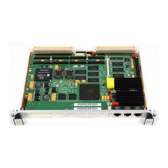
Installation Installation This section discusses the installation of PMCs onto the MVME5100, installation of PMCspan modules onto the MVME5100, and the installation the MVME5100 into a VME chassis. HAWK ASIC Figure 1-1. MVME5100 Layout http://www.motorola.com/computer/literature... -
Page 20: Pmc Modules
Hardware Preparation and Installation PMC Modules PMC modules mount on top of the MVME5100. Perform the following steps to install a PMC module and on your MVME5100. Dangerous voltages, capable of causing death, are present in this equipment. Use extreme caution when handling, testing, and adjusting. -
Page 21: Figure 1-2. Mvme5100 Installation And Removal From A Vmebus Chassis
Installation Figure 1-2. MVME5100 Installation and Removal From a VMEbus Chassis Figure 1-3. Typical PMC Module Placement on an MVME5100 http://www.motorola.com/computer/literature... -
Page 22: Primary Pmcspan
Hardware Preparation and Installation Primary PMCspan To install a PMCspan-002 PCI expansion module on your MVME5100, perform the following steps while referring to the figure on the next page: Dangerous voltages, capable of causing death, are present in this equipment. Use extreme caution when handling, testing, and adjusting. -
Page 23: Figure 1-4. Pmcspan Installation On An Mvme5100
6. Gently press the PMCspan and MVME5100 together and verify that P4 is fully seated in J25. 7. Insert four short screws (Phillips type) through the holes at the corners of the PMCspan and into the standoffs on the MVME5100. Tighten screws securely. http://www.motorola.com/computer/literature... -
Page 24: Secondary Pmcspan
Hardware Preparation and Installation Secondary PMCspan The PMCspan-010 PCI expansion module mounts on top of a PMCspan-002 PCI expansion module. To install a PMCspan-010 on your MVME5100, perform the following steps while referring to the figure on the next page: Dangerous voltages, capable of causing death, are present in this equipment. -
Page 25: Figure 1-5. Pmcspan-010 Installation On A Pmcspan-002/Mvme5100
PMCspan-010 and into the standoffs on the primary PMCspan-002. Tighten screws securely. Note The screws have two different head diameters. Use the screws with the smaller heads on the standoffs next to VMEbus connectors P1 and P2. http://www.motorola.com/computer/literature 1-11... -
Page 26: Mvme5100
Hardware Preparation and Installation MVME5100 Before installing the MVME5100 into your VME chassis, ensure that the jumpers are configured properly. This procedure assumes that you have already installed the PMCspan(s) and any PMCs that you have selected. Perform the following steps to install the MVME5100 in your VME chassis: Dangerous voltages, capable of causing death, are present in this equipment. - Page 27 RF emissions. Note Some VME backplanes (such as those used in Motorola “Modular Chassis” systems) have an auto-jumpering feature for automatic propagation of the IACK and BG signals. The step immediately below does not apply to such backplane designs.
-
Page 28: Introduction
2Operation Introduction This chapter provides operating instructions for the MVME5100 Single Board Computer. It includes necessary information about powering up the system along with the functionality of the switches, status indicators, and I/O ports on the front panels of the board. Switches and Indicators The front panel of the MVME5100 as shown in Figure... -
Page 29: Status Indicators
Operation Additionaly, when the MVME5100 is configured as a System Controller (SCON), a SYSRESET# signal may be generated by toggling the ABT/RST switch to , or by a power-up reset, or by a watchdog timeout, or by a control bit in the Miscellaneous Control Register (MISC_CTL) in the Universe ASIC. -
Page 30: System Powerup
The following flowchart in Figure 2-1 shows the basic initialization process that takes place during MVME5100 system start-ups. For further information on PPCBug, refer to the following: Chapter 3, PPCBug Firmware Appendix B, Troubleshooting Appendix C, Related Documentation http://www.motorola.com/computer/literature... -
Page 31: Figure 2-1. Boot-Up Sequence
Operation Powerup/reset initialization STARTUP Initialize devices on the MVME5100 INITIALIZATION PowerOn SelfTest diagnostics POST Firmware-configured boot mechanism BOOTING so configured. Default is no bo MONITOR Interactive, command-driven on-line PowerPC debugger, when terminal connected. Figure 2-1. Boot-Up Sequence Computer Group Literature Center Web Site... -
Page 32: Introduction
PPCBug Overview The PPCBug (also known as PowerPC debug firmware) is a powerful evaluation and debugging tool for systems built around the Motorola PowerPC microcomputers. Facilities are available for loading and executing user programs under complete operator control for system evaluation. - Page 33 PPCBug Firmware PPCBug includes commands for: Display and modification of memory Breakpoint and tracing capabilities A powerful assembler and disassembler useful for patching programs A self-test at powerup feature which verifies the integrity of the system PPCBug consists of three parts: A command-driven, user-interactive software debugger, described in the PPCBug Firmware Package User’s Manual listed in Appendix C, Related Documentation...
-
Page 34: Implementation And Memory Requirements
After the debugger executes the command, the prompt reappears. However, depending on what the user program does, if the command causes execution of a user target code (i.e. GO), then control may or may not return to the debugger. http://www.motorola.com/computer/literature... -
Page 35: Hardware And Firmware Initialization
PPCBug Firmware For example, if a breakpoint has been specified, then control returns to the debugger when the breakpoint is encountered during execution of the user program. Alternately, the user program could return to the debugger by means of the System Call Handler routine RETURN (described in the PPCBug Firmware Package User’s Manual). - Page 36 22. Displays the debugger’s copyright message. 23. Displays any hardware initialization errors that may have occurred. 24. Checksums the debugger object and displays a warning message if the checksum failed to verify. 25. Displays the amount of local read/write memory found. http://www.motorola.com/computer/literature...
- Page 37 PPCBug Firmware 26. Verifies the configuration data that is resident in NVRAM and displays a warning message if the verification failed. 27. Calculates and displays the MPU clock speed, verifies that the MPU clock speed matches the configuration data, and displays a warning message if the verification fails.
-
Page 38: Default Settings
Primary SCSI Identifier = 07 System Serial Number = nnnnnnn System Identifier = Motorola MVME5100 License Identifier = nnnnnnnn The Board Information Block parameters shown above are left-justified character (ASCII) strings padded with space characters. The Board Information Block is factory-configured before shipment. -
Page 39: Env - Set Environment
PPCBug Firmware ENV - Set Environment Use the ENV command to view and/or configure interactively all PPCBug operational parameters that are kept in Non-Volatile RAM (NVRAM). Refer to the PPCBug Firmware Package User’s Manual for a description of the use of ENV. Additional information on registers in the Universe ASIC that affect these parameters is contained in your MVME5100 Programmer’s Reference Guide listed in Appendix C, Related... - Page 40 Probe System for Supported I/O Controllers [Y/N] = Y? Accesses will be made to the appropriate system buses (e.g., VMEbus, local MPU bus) to determine the presence of supported controllers. (Default) Accesses will not be made to the VMEbus to determine the presence of supported controllers. http://www.motorola.com/computer/literature...
- Page 41 PPCBug Firmware Auto-Initialize of NVRAM Header Enable [Y/N] = Y? NVRAM (PReP partition) header space will be initialized automatically during board initialization, but only if the PReP partition fails a sanity check. (Default) NVRAM header space will not be initialized automatically during board initialization.
- Page 42 Auto Boot Enable [Y/N] = N? The Autoboot function is enabled. The Autoboot function is disabled. (Default) Auto Boot at powerup only [Y/N] = N? Autoboot is attempted at powerup reset only. Autoboot is attempted at any reset. (Default) http://www.motorola.com/computer/literature 3-11...
- Page 43 PPCBug Firmware Auto Boot Scan Enable [Y/N] = Y? If Autoboot is enabled, the Autoboot process attempts to boot from devices specified in the scan list (e.g., ). (Default) FDISK/CDROM/TAPE/HDISK If Autoboot is enabled, the Autoboot process uses the Controller LUN and Device LUN to boot. Auto Boot Scan Device Type List = FDISK/CDROM/TAPE/HDISK? This is the listing of boot devices displayed if the Autoboot Scan option is enabled.
- Page 44 The time value is from BREAK 0-255 seconds. (Default = 5 seconds) ROM Boot Direct Starting Address = FFF00000? The first location tested when PPCBug searches for a ROMboot module. (Default = 0xFFF00000) http://www.motorola.com/computer/literature 3-13...
- Page 45 PPCBug Firmware ROM Boot Direct Ending Address = FFFFFFFC? The last location tested when PPCBug searches for a ROMboot module. (Default = 0xFFFFFFFC) Network Auto Boot Enable [Y/N] = N? The Network Auto Boot (NETboot) function is enabled. The NETboot function is disabled. (Default) Network Auto Boot at power-up only [Y/N] = N? NETboot is attempted at powerup reset only.
- Page 46 DRAM Speed in NANO Seconds = 15? The default setting for this parameter will vary depending on the speed of the DRAM memory parts installed on the board. The default is set to the slowest speed found on the available banks of DRAM memory. http://www.motorola.com/computer/literature 3-15...
- Page 47 PPCBug Firmware ROM Bank A Access Speed (ns) = 80? This defines the minimum access speed for the Bank A Flash Device(s) in nanoseconds. ROM Bank B Access Speed (ns) = 70? This defines the minimum access speed for the Bank B Flash Device(s) in nanoseconds.
-
Page 48: Configuring The Vmebus Interface
PCI Slave Image 0 Bound Address Register = 00000000? The configured value is written into the LSI0_BD register of the Universe chip. PCI Slave Image 0 Translation Offset = 00000000? The configured value is written into the LSI0_TO register of the Universe chip. http://www.motorola.com/computer/literature 3-17... - Page 49 PPCBug Firmware PCI Slave Image 1 Control = C0820000? The configured value is written into the LSI1_CTL register of the Universe chip. PCI Slave Image 1 Base Address Register = 81000000? The configured value is written into the LSI1_BS register of the Universe chip.
- Page 50 VMEbus Slave Image 1 Bound Address Register = 00000000? The configured value is written into the VSI1_BD register of the Universe chip. VMEbus Slave Image 1 Translation Offset = 00000000? The configured value is written into the VSI1_TO register of the Universe chip. http://www.motorola.com/computer/literature 3-19...
- Page 51 PPCBug Firmware VMEbus Slave Image 2 Control = 00000000? The configured value is written into the VSI2_CTL register of the Universe chip. VMEbus Slave Image 2 Base Address Register = 00000000? The configured value is written into the VSI2_BS register of the Universe chip.
-
Page 52: Firmware Command Buffer
DU, ECHO, LO, TA, VE. Note Interactive editing of the startup command buffer is not supported. If changes are needed to an existing set of startup commands, a new set of commands with changes must be reentered. http://www.motorola.com/computer/literature 3-21... -
Page 53: Standard Commands
PPCBug Firmware Standard Commands The individual debugger commands are listed in the following table. The commands are described in detail in the PPCBug Firmware Package User’s Manual listed in Appendix C, Related Documentation. Note You can list all the available debugger commands by entering the Help (HE) command alone. - Page 54 Indirect Block Move IDLE Idle Master MPU I/O Control for Disk I/O Inquiry I/O Physical to Disk I/O “Teach” for Configuring Disk Controller Idle MPU Register Display Idle MPU Register Modify Idle MPU Register Set Load S-Records from Host http://www.motorola.com/computer/literature 3-23...
- Page 55 PPCBug Firmware Table 3-1. Debugger Commands (Continued) Command Description “Alias” for “MM” Command Macro Define/Display Macro Edit Enable Macro Expansion Listing Macro Load Macro Save Memory Display Memory Display (Sector) MENU System Menu Memory Modify Memory Map Diagnostic MMGR Access Memory Manager Memory Set Memory Write Automatic Network Bootstrap Operating...
- Page 56 Remote RESET Cold/Warm Reset Read Loop Register Modify Register Set MPU Execution/Status Switch Directories Set Time and Date SROM SROM Examine/Modify Self Test Symbol Table Attach SYMS Symbol Table Display/Search Trace Terminal Attach TIME Display Time and Date http://www.motorola.com/computer/literature 3-25...
-
Page 57: Diagnostics
PPCBug Firmware Table 3-1. Debugger Commands (Continued) Command Description Transparent Mode Trace to Temporary Breakpoint Verify S-Records Against Memory Revision/Version Display Write Loop Although a command (PFLASH) to allow the erasing and reprogramming of Flash memory is available to you, keep in mind that reprogramming any portion of Flash memory will erase everything currently contained in Caution Flash, including the PPCBug debugger. -
Page 58: Table 3-2. Diagnostic Test Groups
2. Some diagnostics depend on restart defaults that are set up only in a particular restart mode. Refer to the documentation on a particular diagnostic for the correct mode. 3. Test Sets marked with an asterisk (*) are not available on the MVME5100. http://www.motorola.com/computer/literature 3-27... -
Page 59: Introduction
This chapter provides a functional description for the MVME5100 Single Board Computer. The MVME5100 is a high-performance product featuring Motorola’s PowerPlus II architecture with a choice of PowerPC processors—either Motorola’s MPC7400 with AltiVec™ technology for algorithmic intensive computations or the low-power MPC750. - Page 60 Functional Description Table 4-1. MVME5100 General Features (Continued) Feature Specification Memory • EEPROM, on-board programmable • 1MB via two 32-pin PLCC/CLCC sockets; 16MB Surface Mount Main Memory • PC100 ECC SDRAM with 100 MHz bus (SDRAM) • 32MB to 512MB on board, expandable to 1GB via RAM500 memory mezzanine NVRAM •...
-
Page 61: Features Descriptions
PMC products such as the MVME2300 and MVME2400. In MVME761 mode, the MVME5100 is backwards compatible with Motorola's MVME761 transition board originated for use with previous generation single-board computer products such as the MVME2600 and MVME2700. -
Page 62: Figure 4-1. Mvme5100 Block Diagram
Functional Description The following diagram illustrates the architecture of the MVME5100 Single Board Computer. L2 Cache 1M,2M Mezzanine SDRAM System 32MB to 512MB Registers SDRAM TL16C550 32MB to 512MB UART/9pin Processor planar 750 Max Hawk Asic FLASH Clock System Memory Controller (SMC) 1MB to 17MB Generator and PCI Host Bridge (PHB) -
Page 63: Processor
(only 8-bit writes are supported for this bank). Bank A has 4 16-bit Smart Voltage FLASH SMT devices. With 32Mbit flash devices, the flash memory size is 16MB. Note that only 32-bit writes are supported for this bank of flash memory. http://www.motorola.com/computer/literature... -
Page 64: Ecc Sdram Memory
Functional Description ECC SDRAM Memory The MVME5100’s on-board memory and optional memory mezzanines allow for a variety of memory size options. Memory size can be 64 or 512MB for a total of 1GB on-board and mezzanine ECC memory. The memory is controlled by the hardware which provides single-bit error correction and double-bit error detection (ECC is calculated over 72-bits). -
Page 65: Input/Output Interfaces
Refer to the MVME5100 product data sheet for the latest information on the specific device used and to that device’s data sheets for programming and engineering information. http://www.motorola.com/computer/literature... -
Page 66: Timers
Functional Description Timers Timers and counters on the MVME5100 are provided by the board’s hardware (Hawk ASIC). There are four 32-bit timers on the board that may be used for system timing or to generate periodic interrupts. Interrupt Routing Legacy interrupt assignment for the PCI/ISA Bridge is maintained to ensure software compatibility between the MVME5100 and the MVME2700 while in 761 mode. -
Page 67: Introduction
5Pin Assignments Introduction This chapter provides information on pin assignments for various jumpers and connectors on the MVME5100 Single Board Computer. Summary The following tables summarize all of the jumpers and connectors: Jumper Description Connector Description Riscwatch Header IPMC761 Interface Pal Programming Header Memory Expansion Ethernet Port 2... -
Page 68: Jumper Settings
Pin Assignments Jumper Settings The following table provides information about the jumper settings associated with th MVME5100 Single Board Computer. The table below provides a brief description of each jumper and the appropriate setting(s) for proper board operation. Table 5-1. Jumper Switches and Settings Jumper Description Setting... -
Page 69: Connectors
J11. The pin assignments for this connector are as follows: Table 5-2. IPMC761 Connector Pin Assignments Assignment I2CSCL I2CSDA DB8# DB9# DB10# +3.3V +3.3V DB11# DB12# DB13# DB14# +3.3V +3.3V DB15# DBP1# LANINT2_L PIB_INT +3.3V +3.3V PIB_PMCREQ# PIB_PMCGNT# +3.3V +5.0V +5.0V +5.0V +5.0V http://www.motorola.com/computer/literature... -
Page 70: Memory Expansion Connector Pin Assignments
Pin Assignments Memory Expansion Connector (J8) Pin Assignments This connector is used to provide memory expansion capability. A single memory mezzanine card provides a maximum of 256MB of memory. Attaching another memory mezzanine to the first mezzanine provides an additional 512Mbytes of expansion memory. The pin assignments for this connector are as follows: Table 5-3. - Page 71 DQ39 +3.3V +3.3V DQ40 DQ41 DQ42 DQ43 DQ44 DQ45 DQ46 DQ47 DQ48 DQ49 DQ50 DQ51 DQ52 DQ53 +3.3V +3.3V DQ54 DQ55 DQ56 DQ57 DQ58 DQ59 DQ60 DQ61 DQ62 DQ63 CKD00 CKD01 CKD02 CKD03 CKD04 CKD05 +3.3V +3.3V CKD06 CKD07 http://www.motorola.com/computer/literature...
- Page 72 Pin Assignments Table 5-3. Memory Expansion Connector Pin Assignments (Continued) Assignment +3.3V +3.3V CS_C0_L CS_E0_L CS_C1_L CS_E1_L WE_L RAS_L CAS_L +3.3V +3.3V DQMB0 DQMB1 A1_SPD A0_SPD MEZZ1_L MEZZ2_L SDRAMCLK1 SDRAMCLK3 +3.3V SDRAMCLK4 SDRAMCLK2 Note PIN 130, 131, MEZZ1_L, MEZZ2_L, configures the board’s local bus frequency.
-
Page 73: Pci Expansion Connector Pin Assignments
Table 5-4. PCI Expansion Connector Pin Assignments Assignment +3.3V +3.3V PCICLK PMCINTA# PMCINTB# PURST# PMCINTC# HRESET# PMCINTD# TRST# PCIXP# PCIXGNT# PCIXREQ# +12V -12V PERR# SERR# LOCK# SDONE DEVSEL# SBO# TRDY# IRDY# STOP# FRAME# ACK64# Reserved REQ64# Reserved http://www.motorola.com/computer/literature... - Page 74 Pin Assignments Table 5-4. PCI Expansion Connector Pin Assignments (Continued) Assignment PCIRST# C/BE1# C/BE0# C/BE3# C/BE2# AD11 AD10 AD13 AD12 AD15 AD14 AD17 AD16 AD19 AD18 AD21 AD20 AD23 AD22 AD25 AD24 AD27 AD26 AD29 AD28 AD31 AD30 Computer Group Literature Center Web Site...
- Page 75 Assignment PAR64 Reserved C/BE5# C/BE4# C/BE7# C/BE6# AD33 AD32 AD35 AD34 AD37 AD36 AD39 AD38 AD41 AD40 AD43 AD42 AD45 AD44 AD47 AD46 AD49 AD48 AD51 AD50 AD53 AD52 AD55 AD54 AD57 AD56 AD59 AD58 AD61 AD60 AD63 AD62 http://www.motorola.com/computer/literature...
-
Page 76: Pci Mezzanine Card (Pmc) Connectors
Pin Assignments PCI Mezzanine Card (PMC) Connectors These connectors provide 32/64-bit PCI interfaces and P2 I/O for two optional add-on PCI Mezzanine Cards (PMC). The pin assignments for these connectors are as follows: Table 5-5. PMC Slot 1 Connector (J11) Pin Assignments Assignment -12V INTA#... -
Page 77: Table 5-6. Pmc Slot 1 Connector (J12) Pin Assignments
AD09 C/BE0# AD06 AD05 AD04 +5V (Vio) AD03 AD02 AD01 AD00 REQ64# Table 5-6. PMC Slot 1 Connector (J12) Pin Assignments Assignment +12V TRST# Not Used Not Used Not Used Pull-up +3.3V RST# Pull-down +3.3V Pull-down Not Used http://www.motorola.com/computer/literature 5-11... - Page 78 Pin Assignments Table 5-6. PMC Slot 1 Connector (J12) Pin Assignments (Continued) Assignment AD30 AD29 AD26 AD24 +3.3V IDSEL1 AD23 +3.3V AD20 AD18 AD16 C/BE2# Not Used TDRY# +3.3V STOP# PERR# +3.3V SERR# C/BE1# AD14 AD13 AD10 AD08 +3.3V AD07 Not Used +3.3V Not Used...
-
Page 79: Table 5-7. Pmc Slot 1 Connector (J13) Pin Assignments
Table 5-7. PMC Slot 1 Connector (J13) Pin Assignments Assignment Reserved C/BE7# C/BE6# C/BE5# C/BE4# +5V (Vio) PAR64 AD63 AD62 AD61 AD60 AD59 AD58 AD57 +5V (Vio) AD56 AD55 AD54 AD53 AD52 AD51 AD50 AD49 AD48 AD47 AD46 AD45 +5V (Vio) AD44 AD43 AD42 AD41 AD40 http://www.motorola.com/computer/literature 5-13... -
Page 80: Table 5-8. Pmc Slot 1 Connector (J14) Pin Assignments
Pin Assignments Table 5-7. PMC Slot 1 Connector (J13) Pin Assignments (Continued) Assignment AD39 AD38 AD37 AD36 AD35 AD34 AD33 +5V (Vio) AD32 Reserved Reserved Reserved Reserved Table 5-8. PMC Slot 1 Connector (J14) Pin Assignments Assignment Jumper Configurable PMC1_2 (P2-A1) Jumper Configurable PMC1_4 (P2-A2) Jumper Configurable... - Page 81 PMC1_53 (P2-C27) PMC1_54 (P2-A27) PMC1_55 (P2-C28) PMC1_56 (P2-A28) PMC1_57 (P2-C29) PMC1_58 (P2-A29) PMC1_59 (P2-C30) PMC1_60 (P2-A30) PMC1_61 (P2-C31) PMC1_62 (P2-A31) PMC1_63 (P2-C32) PMC1_64 (P2-A32) Note Jumper configuration is dependent upon P2 I/O mode chosen (PMC or MVME761 Mode). http://www.motorola.com/computer/literature 5-15...
-
Page 82: Table 5-9. Pmc Slot 2 Connector (J21) Pin Assignments
Pin Assignments Table 5-9. PMC Slot 2 Connector (J21) Pin Assignments Assignment -12V INTA# INTB# INTC# PMCPRSNT2# INTD# Not Used Not Used PMCGNT2# PMCREQ2# +5V (Vio) AD31 AD28 AD27 AD25 C/BE3# AD22 AD21 AD19 +5V (Vio) AD17 FRAME# IRDY# DEVSEL# LOCK# SDONE# SBO#... -
Page 83: Table 5-10. Pmc Slot 2 Connector (J22) Pin Assignments
AD05 AD04 +5V (Vio) AD03 AD02 AD01 AD00 REQ64# Table 5-10. PMC Slot 2 Connector (J22) Pin Assignments Assignment +12V TRST# Not Used Not Used Not Used Pull-up +3.3V RST# Pull-down +3.3V Pull-down Not Used AD30 AD29 AD26 http://www.motorola.com/computer/literature 5-17... - Page 84 Pin Assignments Table 5-10. PMC Slot 2 Connector (J22) Pin Assignments (Continued) Assignment AD24 +3.3V IDSEL2 AD23 +3.3V AD20 AD18 AD16 C/BE2# Not Used TDRY# +3.3V STOP# PERR# +3.3V SERR# C/BE1# AD14 AD13 AD10 AD08 +3.3V AD07 Not Used +3.3V Not Used Not Used Not Used...
-
Page 85: Table 5-11. Pmc Slot 2 Connector (J23) Pin Assignments
Table 5-11. PMC Slot 2 Connector (J23) Pin Assignments Assignment Reserved C/BE7# C/BE6# C/BE5# C/BE4# +5V (Vio) PAR64 AD63 AD62 AD61 AD60 AD59 AD58 AD57 +5V (Vio) AD56 AD55 AD54 AD53 AD52 AD51 AD50 AD49 AD48 AD47 AD46 AD45 +5V (Vio) AD44 AD43 AD42 AD41 AD40 http://www.motorola.com/computer/literature 5-19... -
Page 86: Table 5-12. Pmc Slot 2 Connector (J24) Pin Assignments
Pin Assignments Table 5-11. PMC Slot 2 Connector (J23) Pin Assignments (Continued) Assignment AD39 AD38 AD37 AD36 AD35 AD34 AD33 +5V (Vio) AD32 Reserved Reserved Reserved Reserved Table 5-12. PMC Slot 2 Connector (J24) Pin Assignments Assignment PMC2_1 (P2-D1) PMC2_2 (P2-Z1) PMC2_3 (P2-D2) PMC2_4 (P2-D3) PMC2_5 (P2-Z3) - Page 87 PMC2_46 (P2-Z31) Not Used Not Used Not Used Not Used Not Used Not Used Not Used Not Used Not Used Not Used Not Used Not Used Not Used Not Used Not Used Not Used Not Used Not Used http://www.motorola.com/computer/literature 5-21...
-
Page 88: Vmebus Connectors P1 And P2 Pin Assignments (Pmc Mode)
Pin Assignments VMEbus Connectors P1 and P2 Pin Assignments (PMC mode) The VMEbus connector P1 provides power and VME signals for 24-bit address and 16-bit data. The pin assignments for the connector are specified by the IEEE P1014-1987 VMEbus Specification and the VME64 Extension Standard. Row B of connector P2 provides power to the MVME5100, and to the upper eight VMEbus address lines, and additional 16 VMEbus data lines. - Page 89 PMC1_53 (J14-53) PMC2_40 (J24-40) PMC1_56 (J14-56) VD29 PMC1_55 (J14-55) PMC2_42 (J24-42) PMC2_44 (J24-44) PMC1_58 (J14-58) VD30 PMC1_57 (J14-57) PMC2_43 (J24-43) PMC1_60 (J14-60) VD31 PMC1_59 (J14-59) PMC2_45 (J24-45) PMC2_46 (J24-46) PMC1_62 (J14-62) PMC1_61 (J14-61) GND PMC1_64 (J14-64) PMC1_63 (J14-63) VPC http://www.motorola.com/computer/literature 5-23...
-
Page 90: Vmebus P1 & P2 Connectors Assignments (Mvme761 Mode)
Pin Assignments VMEbus P1 & P2 Connectors Assignments (MVME761 Mode) The VMEbus connector P1 provides power and VME signals for 24-bit address and 16-bit data. The pin assignments for the connector are specified by the IEEE P1014-1987 VMEbus Specification and the VME64 Extension Standard. -
Page 91: Table 5-14. Vmebus Connector P2 Pin Assignments (Mvme761 Mode)
PMC2_45 (J24-45) PMC2_46 (J24-46) MSYNC# MCLK Note Rows A and C and Z’s (Z1, 3, 5 , 7, 9, 11, 13, 15, and 17) functionality is provided by the IPMC761 in slot 1 and the MVME5100 Ethernet port 2. http://www.motorola.com/computer/literature 5-25... -
Page 92: P2 Input/Output Connector Pin Assignments
Pin Assignments P2 Input/Output Connector Pin Assignments The table below provides connector P2 Input/Output (I/O) mode jumper settings for the PMC P2 I/O mode and the MVME761 P2 I/O mode. For PMC mode, place all jumpers (4) to connect the top row and the middle row. -
Page 93: Com1 And Com2 Connector Pin Assignments
The RJ45 connector is for COM1 and the 9-pin header is for COM2. The pin assignments for these connectors are as follows: Table 5-17. COM1 Connector Pin Assignments Assignment GNDC GNDC GNDC Table 5-18. COM2 Connector Pin Assignments Assignment http://www.motorola.com/computer/literature 5-27... -
Page 94: General Specifications
ASpecifications This appendix lists general specifications and power characteristics for the MVME5100 Single Board Computer. It also provides information on cooling requirements. A complete functional description of the MVME5100 Single Board Computer appears in Chapter 4, Functional Description. Specifications for the optional PMC modules can be found in the documentation for those modules. -
Page 95: Power Requirements
100 CFM axial fan. Note that 400 LFM (Linear Feet per Minute) of forced air cooling is recommended for operation in the upper temperature range Temperature qualification is performed in a Motorola development chassis. Twenty-five–watt load boards are inserted in two card slots, one on each side, adjacent to the board under test, to simulate a high power density system configuration. - Page 96 71° C with increased airflow. It is important to note that there are several factors, in addition to the rated CFM of the air mover, which determine the actual volume and speed of air flowing over a module. http://www.motorola.com/computer/literature...
-
Page 97: Solving Startup Problems
BTroubleshooting Solving Startup Problems In the event of difficulty with your MVME5100, perform the simple troubleshooting steps listed in the table below before calling for help or sending the board back for repair. Some of the procedures will return the board to the factory debugger environment. - Page 98 Solving Startup Problems Table B-1. Troubleshooting Problems (Continued) Condition Possible Problem Possible Resolution: II. There is a display A. The keyboard or Recheck the keyboard and/or mouse connections and on the terminal; mouse may be power. however, keyboard connected and/or mouse input incorrectly.
- Page 99 Or, it may indicate a test that failed. If neither happens, enter: de <CR> Any errors should now be displayed. If there are any errors, go to step VI. If there are no errors, go to step V. http://www.motorola.com/computer/literature...
- Page 100 Solving Startup Problems Table B-1. Troubleshooting Problems (Continued) Condition Possible Problem Possible Resolution: V. The debugger is in A. No apparent No further troubleshooting steps are required. system mode; the problems — board autoboots, troubleshooting is or the board has done.
-
Page 101: Motorola Computer Group Documents
CRelated Documentation Motorola Computer Group Documents The Motorola publications listed below are referenced in this manual. You can obtain paper or electronic copies of Motorola Computer Group publications by: Contacting your local Motorola sales office Visiting Motorola Computer Group’s World Wide Web literature site, http://www.motorola.com/computer/literature... -
Page 102: Manufacturers' Documents
Table C-2. Manufacturers’ Documents Publication Document Title Number MPC750 RISC Microprocessor Users Manual MPC750UM/AD Motorola Literature Distribution Center Telephone: (800) 441-2447 or (303) 675-2140 MPC7400 RISC Microprocessor Users Manual MPC7400UM/D Motorola Literature Distribution Center Telephone: (800) 441-2447 or (303) 675-2140... -
Page 103: Related Specifications
FAX: (503) 234-6762 Common Mezzanine Card Specification P1386 IEEE Standards Department Draft 2.0 445 Hoes Lane, P.O Box 1331 Piscataway, NJ 08855-1331 PCI Mezzanine Card Specification P1386.1 IEEE Standards Department Draft 2.0 445 Hoes Lane, P.O Box 1331 Piscataway, NJ 08855-1331 http://www.motorola.com/computer/literature... - Page 104 Index Abort (interrupt) signal CNFG ABT switch (S1) COM1 Interface air temperature COM2 Interface AltiVec™ technology commands assembly language PPCBug Asynchronous Communications debugger 3-22 Auto Boot configurable items Abort Delay 3-13 configure Controller 3-12 PPCBug parameters Default String 3-13 VMEbus interface 3-17 Device 3-12...
- Page 105 Index global bus timeout SDRAM Memory EEPROM hardware configuration Auto Boot Abort Delay 3-13 diagnostics 3-26 Auto Boot Controller 3-12 initialization Auto Boot Default String 3-13 Hawk System Memory Controller Auto Boot Device 3-12 HE (Help) command 3-26 Auto Boot Partition Number 3-12 humidity L2 Cache Parity Enable...
- Page 106 Primary SCSI Data Bus Width 3-11 Primary SCSI Data Bus Width 3-11 Processor ROM Boot Enable 3-13 product specifications SCSI bus reset on debugger startup 3-10 prompt, debugger 3-26 Secondary SCSI identifier 3-11 prompts Operation Mode Jumpers PPCBug http://www.motorola.com/computer/literature IN-3...
- Page 107 Index Real-Time Clock & NVRAM & Universe VMEbus interface ASIC Watchdog Timer uppercase 3-27 required equipment using the front panels RESET and ABORT Switch resetting the system VMEbus restart mode 3-27 VMEbus interface 4-7, 5-1 Riscwatch Header Programmable DMA Controller ROM Boot Enable 3-13 SCSI bus...
Need help?
Do you have a question about the AltiVec MVME5100 Series and is the answer not in the manual?
Questions and answers