Table of Contents
Advertisement
Quick Links
This supplement provides additional information about the MVME1603 and
MVME1604 boards.
The attached pages are replacements for the corresponding pages in the manual.
A vertical bar (|) in the margin of replacement pages indicates where a change
was made.
The supplement number is shown at the bottom of each new page.
Please replace the pages according to the following table:
Remove Existing Pages
Preface/Copyright
vii/viii through ix/x
1-37/1-38 through 1-41/1-42
3-7/3-8 through 3-9/3-10
3-23/3-24 through 3-25/3-26
Place this page behind the title page of the manual as a record of this change.
Supplement to
MVME1603/MVME1604
Single Board Computer
Installation and Use
(V1600-1A/IH3)
1-33/1-34
3-1/3-2
Insert New Pages
Preface/Copyright
vii/viii through ix/x
1-33/1-34
1-37/1-38 through 1-41/1-42
3-1/3-2
3-7/3-8 through 3-9/3-10
3-23/3-24 through 3-25/3-26
V1600-1A/IH3A1
February 1997
Advertisement
Table of Contents

Related Manuals for Motorola MVME1603


Summary of Contents for Motorola MVME1603
- Page 1 Single Board Computer Installation and Use (V1600-1A/IH3) This supplement provides additional information about the MVME1603 and MVME1604 boards. The attached pages are replacements for the corresponding pages in the manual. A vertical bar (|) in the margin of replacement pages indicates where a change was made.
- Page 2 Motorola, Inc. assumes no liability resulting from any omissions in this document, or from the use of the information obtained therein. Motorola reserves the right to revise this document and to make changes from time to time in the content hereof without obligation of Motorola to notify any person of such revision or changes.
- Page 3 MVME1603/MVME1604 Single Board Computer Installation and Use V1600-1A/IH3...
- Page 4 Motorola, Inc. assumes no liability resulting from any omissions in this document, or from the use of the information obtained therein. Motorola reserves the right to revise this document and to make changes from time to time in the content hereof without obligation of Motorola to notify any person of such revision or changes.
- Page 5 Related Documentation section in Appendix A of this manual. The MVME1603/1604 family of Single Board Computers has two parallel branches based on two distinct versions of the base board. Both versions are populated with a number of similar plug-together components, which are listed in the following table.
- Page 6 Motorola symbol are registered trademarks of Motorola, Inc. AIX™ is a trademark of IBM Corp. PowerPC™ is a trademark of IBM Corp. and is used by Motorola with permission. All other products mentioned in this document are trademarks or registered trademarks of their respective holders.
- Page 7 Motorola, Inc. assumes no liability for the customer’s failure to comply with these requirements. The safety precautions listed below represent warnings of certain dangers of which Motorola is aware. You, as the user of the product, should follow these warnings and all other safety precautions necessary for the safe operation of the equipment in your operating environment.
- Page 8 All Motorola PWBs (printed wiring boards) are manufactured by UL-recognized manufacturers, with a flammability rating of 94V-0. This equipment generates, uses, and can radiate electro- magnetic energy. It may cause or be susceptible to electro-magnetic interference (EMI) if not installed and WARNING used in a cabinet with adequate EMI protection.
-
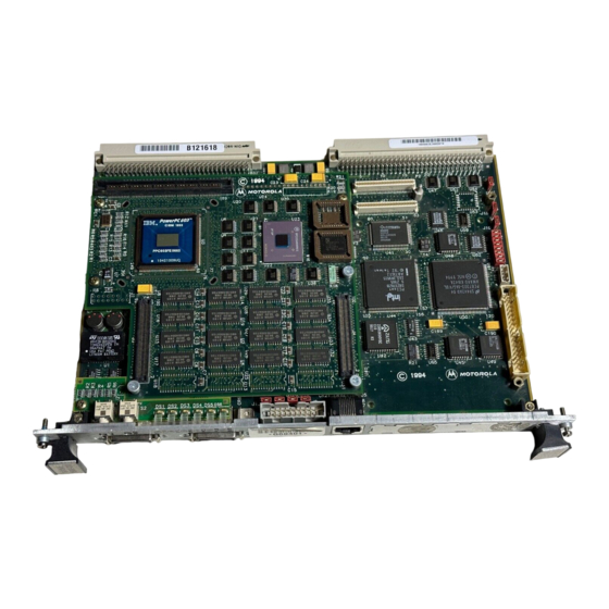
Page 9: 1Hardware Preparation And Installation
The differences between the MVME1600-001 and the MVME1600-011 lie mainly in the area of I/O handling; the logic design is the same for both versions. In either case, the complete MVME1603/1604 consists of the base board plus: A processor/memory module (PM603 or PM604) with... -
Page 10: Equipment Required
Equipment Required Equipment Required The following equipment is required to complete an MVME1603/ 1604 system: VME system enclosure System console terminal Transition module (MVME760 for the MVME1600-001 base boards, MVME712M for the MVME1600-011) and connecting cables Disk drives (and/or other I/O) and controllers... - Page 11 Hardware Preparation and Installation MOUSE DB15 68-PIN CONNECTOR TERMINATORS GRAPHICS SCSI CL-GD5434 NCR-53C825 DRAM 256Kx16 PCI LOCAL BUS TO MPU MODULE ETHERNET S82378ZB VME2PCI DECchip ISA BRIDGE BRIDGE 21040 PMC SLOT 10BT ISA BUS PC87303 DECODE SUPER I/O FUNCTION VMEchip2 ESCC MK48T18 85230...
- Page 12 Equipment Required HD26 HD26 RJ45 TO MPU MODULE 10BT PMC SLOT PCI LOCAL BUS EIA232 ETHERNET ESCC S82378ZB SCSI VME2PCI DECchip 85230 Z8536 ISA BRIDGE NCR-53C810 BRIDGE 21040 ISA BUS PC87303 CSRs SUPER I/O MK48T18 VMEchip2 BUFFERS P2 CONNECTOR P1 CONNECTOR 11199.00 9502 Figure 1-2.
-
Page 13: Overview Of Startup Procedure
For more information on optional devices and equipment, refer to the documentation provided with the equipment. Power up the system. Switches and LEDs Troubleshooting the MVME1603/1604; Solving Start-Up Problems Note that the debugger Using the Debugger prompt appears. You may also wish to obtain the PPCBug Firmware Package User’s Manual, listed in... -
Page 14: Unpacking Instructions
Caution Hardware Configuration To produce the desired configuration and ensure proper operation of the MVME1603/1604, you may need to carry out certain modifications before installing the module. The MVME1603/1604 provides software control over most options: by setting bits in control registers after installing the MVME1603/ 1604 in a system, you can modify its configuration. -
Page 15: Scsi Bus Terminator Selection (J7)
Hardware Preparation and Installation MVME1600-001 Base Board Preparation Figure 1-3 illustrates the placement of the switches, jumper headers, connectors, and LED indicators on the MVME1600-001. Manually configurable items on the base board include: SCSI bus terminator selection (J7) General-purpose software-readable header (J8) VMEbus system controller selection (J9) Serial Port 3 clock configuration (J10) Serial Port 4 clock configuration (J13) -
Page 16: General-Purpose Software-Readable Header (J8)
MVME1600-001 Base Board Preparation General-Purpose Software-Readable Header (J8) Header J8 provides eight readable jumpers. These jumpers can be read as a register at ISA I/O address $80000801. Bit 0 is associated with header pins 1 and 2; bit 7 is associated with pins 15 and 16. The bit values are read as a zero when the jumper is installed, and as a one when the jumper is removed. -
Page 17: Console Port Configuration
Hardware Preparation and Installation Console Port Configuration On the MVME1600-001 base board, either the standard serial console port ( ) or the on-board video (VGA) port can serve as COM1 the PPCBug firmware console port. The firmware checks for the presence of a connected keyboard and a connected mouse. -
Page 18: Vmebus System Controller Selection (J9)
Parity disabled (no parity) Baud rate of 9600 baud 9600 baud is the power-up default for serial ports on MVME1603/ 1604 boards. After power-up you can reconfigure the baud rate if you wish, via the PPCBug firmware’s Port Format (PF) command. -
Page 19: Serial Port 3 Clock Configuration (J10)
Hardware Preparation and Installation Serial Port 3 Clock Configuration (J10) You can configure Serial port 3 on the MVME1600-001 to use the clock signals provided by the TXC signal line. Header J10 configures port 3 to either drive or receive TXC. The factory configuration has port 3 set to receive TXC. - Page 20 MVME1600-001 Base Board Preparation MVME 1600-001 Figure 1-3. MVME1600-001 Switches, Headers, Connectors, Fuses, LEDs 1-12...
-
Page 21: Serial Port 4 Clock Configuration (J13)
Hardware Preparation and Installation Serial Port 4 Clock Configuration (J13) You can configure Serial port 4 on the MVME1600-001 to use the clock signals provided by the TXC signal line. Header J13 configures port 4 to either drive or receive TXC. The factory configuration has port 4 set to receive TXC. - Page 22 MVME1600-001 Base Board Preparation Table 1-2 lists the pin numbers, signal mnemonics, and signal descriptions for J1. Table 1-2. Remote Reset Connector J1 Interconnect Signals Signal Signal Name and Description Number Mnemonic Not used. ∗ RESETSW RESET Switch. Signal goes low when the RESET switch is pressed.
-
Page 23: Mvme760 Transition Module Preparation
Hardware Preparation and Installation MVME760 Transition Module Preparation The MVME760 transition module (Figure 1-4) is used in conjunction with the MVME1600-001 base board. The features of the MVME760 include: A parallel printer port An Ethernet interface supporting both AUI and 10BaseT connections Two EIA-232-D asynchronous serial ports (identified as COM1... - Page 24 MVME760 Transition Module Preparation You can change Serial Ports 3 and 4 from an EIA-232-D to an EIA- 530 interface (or vice-versa) by mounting the appropriate SIM705 series interface module and setting the corresponding jumper. SIMs can be ordered separately as required. Headers J9 and J8 are used to configure Serial Port 3 and Serial Port 4, respectively.
- Page 25 Hardware Preparation and Installation MVME 760-001 1551 9410 Figure 1-4. MVME760 Connector and Header Locations 1-17...
-
Page 26: Serial Port 4 Dce/Dte Selection (J7)
MVME1600-011 Base Board Preparation MVME1600-011 Base Board Preparation Figure 1-5 illustrates the placement of the switches, jumper headers, connectors, and LED indicators on the MVME1600-011. Manually configurable items on the base board include: Serial Port 4 DCE/DTE selection (J7) Serial Port 4 clock selection (J8, J15, J16) Serial Port 4 I/O path selection (J9) VMEbus system controller selection (J10) Serial Port 3 I/O path selection (J13) - Page 27 Hardware Preparation and Installation MVME 1600-011 Figure 1-5. MVME1600-011 Switches, Headers, Connectors, Fuses, LEDs 1-19...
-
Page 28: Serial Port 4 Clock Selection (J8/15/16)
MVME1600-011 Base Board Preparation Serial Port 4 Clock Selection (J8/15/16) The MVME1600-011 is shipped from the factory with Serial Port 4 configured for asynchronous communications (i.e., the internal clock is used). Port 4 can be configured for synchronous communications as well. It can either drive (using the internal clock) or receive (using an external clock) the Receive and Transmit clock signals. -
Page 29: Serial Port 4 I/O Path Selection (J9)
Hardware Preparation and Installation To complete the configuration of the clock lines, you must also set serial port 4 clock configuration header J15 on the MVME712M transition module (described later in this chapter). For details on the configuration of that header, refer to the MVME712M Transition Module section or to the user’s manual for the MVME712M (part number MVME712M). -
Page 30: Vmebus System Controller Selection (J10)
MVME1600-011 Base Board Preparation VMEbus System Controller Selection (J10) The MVME1600-011 is factory-configured in system controller mode (i.e., a jumper is installed across pins 2 and 3 of header J10). This means that the MVME1600-011 assumes the role of system controller at system power-up or reset. -
Page 31: Serial Port 3 I/O Path Selection (J13)
Hardware Preparation and Installation Serial Port 3 I/O Path Selection (J13) On the MVME1600-011, serial port 3’s I/O signals are routed to backplane connector P2 and to front panel connector J2. Header J13 determines the state of the DSR, RI, and TM signals on serial port 3. With a jumper installed on J13, DSR, RI, and TM come from the front panel. - Page 32 MVME1600-011 Base Board Preparation Low-Order Bit Pins Definition Bit #0 (SRH0) 1—2 Reserved for future use. Bit #1 (SRH1) 3—4 With the jumper installed between pins 3 and 4 (factory configuration), the debugger uses the current user setup/operation parameters in NVRAM.
- Page 33 Hardware Preparation and Installation Remote Status and Control The remote status and control connector, J4, is a keyed double-row 20-pin connector located behind the front panel of the MVME1600- 011. It connects to a user-supplied external cable and carries the signals for remote reset, abort, the LEDs, and three general-purpose I/O signals.
- Page 34 MVME1600-011 Base Board Preparation Table 1-3. Remote Reset Connector J4 Interconnect Signals Signal Signal Name and Description Number Mnemonic +5VRMT +5 Vdc Power. Fused through fuse F1; +5 Vdc power to a user-supplied external connection. ∗ LANLED LAN LED. Signal goes low when the illuminates.
-
Page 35: Mvme712M Transition Module Preparation
Hardware Preparation and Installation MVME712M Transition Module Preparation The MVME712M transition module (Figure 1-6) and P2 adapter board are used in conjunction with the MVME1600-011 base board. The features of the MVME712M include: A parallel printer port (through the P2 adapter) An Ethernet interface supporting AUI connections (through the P2 adapter) Four EIA-232-D multiprotocol serial ports (through the P2... - Page 36 MVME712M Transition Module Preparation MVME712M Figure 1-6. MVME712M Connector and Header Locations 1-28...
-
Page 37: Serial Ports 1-4 Dce/Dte Configuration
Hardware Preparation and Installation Serial Ports 1-4 DCE/DTE Configuration Serial ports 1 through 4 are configurable as modems (DCE) for connection to terminals, or as terminals (DTE) for connection to modems. The MVME712M is shipped with the serial ports configured for DTE operation. Serial port DCE/DTE configuration is accomplished by positioning jumpers on one of two headers per port.The following table lists the serial ports with their corresponding jumper headers. - Page 38 MVME712M Transition Module Preparation MVME712M FRONT 64 PIN ADAPTER TRANSITION PANEL CABLE HD26 BOARD BOARD DB25 Z85230 SCC TXDB RTSB* RXDB CTSB* DCDB* TRXC4 RTXC TXCI RRXC TTXC TXCO TRXCB RTXC4 RXCI RTXCB Z8536 CIO (PB5) DTR4* RXDB (PB3) LLB4* DCDB* (PB4) RLB4* CTSB*...
- Page 39 Hardware Preparation and Installation Preparation of the P2 adapter for the MVME712M consists of removing or installing the SCSI terminating resistors. Figure 1-9 illustrates the location of the resistors, fuse, and connectors. For further information on the preparation of the transition module and the P2 adapter, refer to the user’s manual for the MVME712M (part number MVME712M) as necessary.
-
Page 40: Hardware Installation
The following sections discuss the placement of the various mezzanine cards on the the MVME1600-001 and the MVME1600- 011 base boards, the installation of the complete MVME1603/1604 VMEmodule assembly and corresponding transition module into a VME chassis, and the system considerations relevant to the installation. - Page 41 Hardware Preparation and Installation PM603/604 Processor/Memory Mezzanine To install a PM603 or PM604 processor/memory mezzanine on an MVME1603/1604 main module, refer to Figure 1-10 and proceed as follows: 1. Attach an ESD strap to your wrist. Attach the other end of the ESD strap to the chassis as a ground.
- Page 42 PM603/604 Processor/Memory Mezzanine PM603/PM604 11197.00 9411 (1-2) Figure 1-10. PM603/PM604 Placement on MVME1603/1604 1-34...
-
Page 43: Ram104 Memory Mezzanine Installation
Hardware Preparation and Installation 5. Align the standoffs on the MVME1603/1604 board with the holes at the edges of the PM603 or PM604 mezzanine, insert the Phillips screws through the holes in the mezzanine and the spacers, and tighten the screws. - Page 44 RAM104 Memory Mezzanine Installation RAM104 PM603/PM604 Figure 1-11. RAM104 Placement on PM603/PM604 1-36...
- Page 45 Hardware Preparation and Installation 3. Carefully remove the MVME1603/1604 from its VMEbus card slot and lay it flat on an ESD mat, component side up, with connectors P1 and P2 facing you and the PM603/PM604 corner cutout at the upper right. The ESD mat should be on a firm, flat surface.
- Page 46 MVME1603/1604 VMEmodule Installation With mezzanine boards installed and headers properly configured, proceed as follows to install the MVME1603/1604 in the VME chassis: 1. Attach an ESD strap to your wrist. Attach the other end of the ESD strap to the chassis as a ground. The ESD strap must be secured to your wrist and to ground throughout the procedure.
- Page 47 The system controller must be in slot 1 to correctly initiate the bus-grant daisy-chain and to ensure proper operation of the IACK daisy-chain driver. – If you do not intend to use the MVME1603/1604 as system controller, it can occupy any unused double-height card slot.
-
Page 48: Mvme760 Transition Module Installation
MVME760 Transition Module Installation MVME760 Transition Module Installation The MVME760 transition module is used in conjunction with the MVME1600-001 base board. With the MVME1603/1604 installed, refer to Figure 1-12 and proceed as follows to install an MVME760 transition module: 1. Attach an ESD strap to your wrist. Attach the other end of the ESD strap to the chassis as a ground. - Page 49 AC or DC power source, and turn the equipment power on. Not all peripheral cables are provided with the Note MVME760; you may need to fabricate or purchase certain cables. (Motorola recommends shielded cable for all peripheral connections to minimize radiation.) MVME760 MVME1600-001 ENCLOSURE BOUNDARY 1548 9412 Figure 1-12.
-
Page 50: Mvme712M Transition Module Installation
MVME712M Transition Module Installation MVME712M Transition Module Installation The MVME712M transition module is used in conjunction with the MVME1600-011 base board. With the MVME1603/1604 installed, refer to Figure 1-13 and proceed as follows to install an MVME712M transition module: 1. Attach an ESD strap to your wrist. Attach the other end of the ESD strap to the chassis as a ground. - Page 51 AC or DC power source, and turn the equipment power on. Note Not all peripheral cables are provided with the MVME712M; you may need to fabricate or purchase certain cables. (Motorola recommends shielded cable for all peripheral connections to minimize radiation.) 1-43...
- Page 52 MVME712M Transition Module Installation TERMINATORS SCSI INSTALLED DEVICE SCSI DEVICE MVME712M MVME1600-011 50-CONDUCTOR CABLE 64-CONDUCTOR CABLE P2 ADAPTER TERMINATORS TERMINATORS REMOVED INSTALLED ENCLOSURE BOUNDARY cb2349301 Figure 1-13. MVME712M/MVME1600-011 Cable Connections 1-44...
-
Page 53: System Considerations
VMEbus backplane connectors P1 and P2. Whether the MVME1603/1604 operates as a VMEbus master or as a VMEbus slave, it is configured for 32 bits of address and 32 bits of data (A32/D32). However, it handles A16 or A24 devices in the address ranges indicated in Chapter 2. - Page 54 GCSR (global control/status register) set includes four bits that function as location monitors to allow one MVME1603/1604 processor to broadcast a signal to any other MVME1603/1604 processors. All eight registers are accessible from any local processor as well as from the VMEbus.
- Page 55 Hardware Preparation and Installation In addition, the MVME1600-001 base board provides +5Vdc to the SCSI bus signal through fuse F1, located near the front TERMPWR panel SCSI connector. The LED (DS5) on the front panel monitors the SCSI bus signal along with the other TERMPWR operating voltages;...
- Page 56 System Considerations The MVME1600-011 base board supplies SCSI terminator power through a 1A fuse (F1) located on the P2 adapter board. If the fuse is blown, the SCSI device(s) may function erratically or not at all. With the P2 adapter board cabled to an MVME712M and with an SCSI bus connected to the MVME712M, the green DS2 LED on the MVME712M illuminates when SCSI terminator power is available.
-
Page 57: Functional Description
This chapter describes the MVME1603/MVME1604 single-board computer on a block diagram level. The General Description provides an overview of the MVME1603/MVME1604, followed by a detailed description of several blocks of circuitry. Figure 3-1 shows a block diagram of the overall board architecture. - Page 58 Features Table 3-1. MVME1603/MVME1604 Features (Continued) Feature Description Models Real-time clock 8KB NVRAM with RTC and battery All models backup (SGS-Thomson M48T18) Switches All models RESET ABORT Status LEDs Six: All models Tick timers Four programmable 16-bit timers (one in All models S82378ZB ISA bridge;...
-
Page 59: General Description
MVME1603 is equipped with a PowerPC 603 microprocessor; the MVME1604 has a PowerPC 604. 256KB L2 cache memory is available as an option on certain models of the MVME1603 and the MVME1604. The MVME1603/1604 family has two parallel branches based on two distinct versions (MVME1600-001 and MVME1600-011) of the base board. -
Page 60: Block Diagram
Its flexible mezzanine architecture allows relatively easy upgrades of the processor and/or memory. A key feature of the MVME1603/MVME1604 family is the PCI (Peripheral Component Interconnect) bus. In addition to the on- board local bus peripherals, the PCI bus supports an industry- standard mezzanine interface, IEEE P1386.1 PMC (PCI Mezzanine... - Page 61 SCSI VIDEO DECchip PMC SLOT VMEchip2 NCR-53C8xx CL-GD5434 21040 MVME1600-001 / 011 BASE BOARD NOTES : 1. SHADED BOXES ARE MVME1600-001 FEATURES ONLY. 2. SCSI CONTROLLER IS NCR-53C825 ON MVME1600-001, NCR-53C810 ON -011. 11186.00 9606 Figure 3-1. MVME1603/MVME1604 Block Diagram...
-
Page 62: Scsi Interface
VMEbus signal noise at P2. The SCSI bus is 16 bits wide in MVME1600-001-based versions of the MVME1603/MVME1604, and 8 bits wide in MVME1600-011- based versions. Refer to Chapter 4 for the pin assignments of the MVME1600-001 front panel SCSI connector. -
Page 63: Ethernet Interface
Functional Description MVME1603/MVME1604 module, then SCSI termination must be enabled. +5Vdc power to the SCSI bus signal and TERMPWR termination resistors is supplied through a fuse (F1) and diode. The MVME1600-011 base board uses the sockets provided for SCSI bus terminators on the P2 adapter board. If the SCSI bus ends at the adapter board, then termination resistors must be installed on the adapter board. -
Page 64: Graphics Interface
$FFFC1F2C, the upper four bytes (08003E2x) can be read. At an address of $FFFC1F30, the lower two bytes (xxxx) can be read. The MVME1603/MVME1604 debugger, PPCBug, has the capability to retrieve or set the Ethernet station address. If the data in the NVRAM is lost, use the number on the label on backplane connector P2 to restore it. -
Page 65: Pci Mezzanine Interface
Technical Reference Manual for detailed programming information. PCI Mezzanine Interface A key feature of the MVME1603/MVME1604 family is the PCI (Peripheral Component Interconnect) bus. In addition to the on- board local bus devices (SCSI, Ethernet, graphics, etc.), the PCI bus supports an industry-standard mezzanine interface, IEEE P1386.1... -
Page 66: Vmebus Interface
MVME1603/MVME1604 Programmer’s Reference Guide. ISA Super I/O Device (ISASIO) The MVME1603/MVME1604 uses a PC87303 ISASIO chip from National Semiconductor to implement certain segments of the P2 and front-panel I/O: Two asynchronous serial ports (COM1 and COM2) via P2... - Page 67 IBC (ISA/PCI Bridge Controller) interrupt request line IRQ7. You can change the default configuration by reprogramming the ISASIO device. For detailed programming information, refer to the PCI and ISA bus discussions in the MVME1603/MVME1604 Programmer’s Reference Guide and to the vendor documentation for the ISASIO device.
-
Page 68: Isa Bridge Controller
ISA Bridge Controller The MVME1603/MVME1604 uses an Intel S82378ZB bridge controller to supply the interface between the PCI local bus and the ISA system I/O bus (diagrammed in Figure 1-1 and Figure 1-2 for the two base boards). -
Page 69: Real-Time Clock And Nvram
$00800800 in the PCI Configuration area. Real-Time Clock and NVRAM The MVME1603/MVME1604 employs an SGS-Thomson surface- mount M48T18 RAM and clock chip to provide 8KB of non-volatile static RAM and a real-time clock. This chip provides a clock,... -
Page 70: Programmable Timers
Although the M48T18 is an 8-bit device, 8-, 16-, and 32- bit accesses from the ISA bus to the M48T18 are supported. Refer to the MVME1603/MVME1604 Programmer’s Reference Guide and to the M48T18 data sheet for detailed programming and battery life information. -
Page 71: Serial Communications Interface
Functional Description The interval timers use the OSC clock input as their clock source. The MVME1603/MVME1604 module drives the OSC pin with a 14.31818 MHz clock source. 16-Bit Timers Four 16-bit timers are available on the MVME1603/MVME1604. The ISA bridge controller supplies one 16-bit timer; the Z8536 CIO device provides the other three. - Page 72 Z85230 according to the interrupt source. Interrupt request levels are programmed via the ISA bridge controller. Refer to the Z85230 data sheet and to the MVME1603/ MVME1604 Programmer’s Reference Guide for further information. Z8536 CIO Device...
-
Page 73: Board Configuration Register
Functional Description Board Configuration Register The Board Configuration Register is an 8-bit read-only register containing the details of the MVME1603/MVME1604 single-board computer’s configuration. This register is located on the base board at ISA I/O address $0802. Board Configuration Register - $0802 ∗... -
Page 74: P2 Signal Multiplexing
Block Diagram P2 Signal Multiplexing Due to the limited availability of pins in the P2 backplane connector, the MVME1600-001 base board multiplexes and demultiplexes certain synchronous I/O control signals that pass between the base board and the MVME760 transition module. This is a hardware function that is entirely transparent to software. - Page 75 The interrupt is normally used to abort program execution and return control to the PPCBug debugger firmware located in the MVME1603/1604 EPROM and Flash memory. The interrupt signal reaches the processor module via ISA bus interrupt line IRQ8 ∗...
- Page 76 RESET switch resets all onboard devices; it also drives a ∗ signal if SYSRESET the MVME1603/1604 is the system controller. The switch RESET may be disabled by software. The VMEchip2 includes both a global and a local reset driver. When the VMEchip2 operates as the VMEbus system controller, the...
-
Page 77: Front Panel Indicators (Ds1 - Ds6)
Functional Description Front Panel Indicators (DS1 - DS6) There are six LEDs on the MVME1603/1604 front panel: , and (DS1, yellow). Checkstop; driven by the MPC603/604 status lines on the MVME1603/1604. Lights when a halt condition from the processor is detected. -
Page 78: Polyswitches (Resettable Fuses)
Block Diagram Polyswitches (Resettable Fuses) The MVME1600-001 and MVME1600-011 base boards draw fused +5Vdc, +12Vdc, and –12Vdc power from the VMEbus backplane through connectors P1 and P2. The 3.3Vdc power (used by the ISA Super I/O device on the base board, and by the PM603 or PM604 processor/memory mezzanine) is derived on-board from the +5Vdc. - Page 79 Functional Description Note Because any device on the SCSI bus can provide , and because the LED monitors the status TERMPWR of several voltages, the LED does not directly indicate the condition of any single fuse. If the LED flickers or goes out, check all the fuses (polyswitches).
-
Page 80: Speaker Control
Block Diagram Speaker Control The MVME1600-001 base board supplies a signal to SPEAKER_OUT the 14-pin combined LED-mezzanine/remote-reset connector, J1. When J1 is used as a remote reset connector with the LED mezzanine removed, the signal can be cabled to an SPEAKER_OUT external speaker to obtain a beep tone. - Page 81 Functional Description kept on the processor bus to get the optimum performance from the designs. Electrically, the processor/memory module is a PCI connection. MPC604 boards have double-wide front panels to accommodate a heat sink on the PowerPC604 that protrudes into the adjacent VME slot.
-
Page 82: Ram104 Memory Module
(together with a PM603 or PM604 processor/memory mezzanine, an LED mezzanine, and an optional PCI mezzanine card) plugs into the base board to make a complete MVME1603 or MVME1604 single-board computer. See Figure 1-11. RAM104 modules of 8, 16, 32, or 64MB are available for memory expansion. -
Page 83: Mvme760 Transition Module
Functional Description MVME760 Transition Module The MVME760 transition module (Figure 1-4) is used in conjunction with the MVME1600-001 base board. The features of the MVME760 include: A parallel printer port An Ethernet interface supporting both AUI and 10BaseT connections Two EIA-232-D asynchronous serial ports (identified as COM1 on the front panel) COM2... -
Page 84: Mvme712M Transition Module
Block Diagram MVME712M Transition Module The MVME712M transition module (Figure 1-6) and P2 adapter board are used in conjunction with the MVME1600-011 base board. The features of the MVME712M include: A parallel printer port (through the P2 adapter) An Ethernet interface supporting AUI connections (through the P2 adapter) Four EIA-232-D multiprotocol serial ports (through the P2 adapter)
Need help?
Do you have a question about the MVME1603 and is the answer not in the manual?
Questions and answers