Motorola MVME2600 Series Programmer's Reference Manual
Hide thumbs
Also See for MVME2600 Series:
- Reference manual (283 pages) ,
- Installation and use manual (198 pages) ,
- Installation and use manual (20 pages)
Advertisement
Quick Links
Advertisement

Related Manuals for Motorola MVME2600 Series


Summary of Contents for Motorola MVME2600 Series
- Page 1 MVME2600 Series Single Board Computer Programmer’s Reference Guide V2600A/PG1...
- Page 2 Motorola, Inc. assumes no liability resulting from any omissions in this document, or from the use of the information obtained therein. Motorola reserves the right to revise this document and to make changes from time to time in the content hereof without obligation of Motorola to notify any person of such revision or changes.
- Page 3 Preface The MVME2600 Series Single Board Computer ProgrammerÕs Reference Guide provides brief board level information, complete memory maps, and detailed ASIC chip information including register bit descriptions for the MVME2600 series Single Board Computers (also called MVME2603 and MVME2604 in this manual). The information contained in this manual applies to the single board computers built from some of the plug-together components listed in the following table.
- Page 4 The computer programs stored in the Read Only Memory of this device contain material copyrighted by Motorola Inc., Þrst published 1990, and may be used only under a license such as the License for Computer Programs (Article 14) contained in Motorola's Terms and Conditions of Sale, Rev. 1/79.
- Page 5 Motorola, Inc. assumes no liability for the customer's failure to comply with these requirements. The safety precautions listed below represent warnings of certain dangers of which Motorola is aware. You, as the user of the product, should follow these warnings and all other safety precautions necessary for the safe operation of the equipment in your operating environment.
- Page 7 Contents Introduction 1-1 Manual Terminology 1-1 Overview 1-3 Feature Summary 1-3 System Block Diagram 1-4 Functional Description 1-6 Overview 1-6 Programming Model 1-7 Memory Maps 1-7 Processor Memory Maps 1-7 PCI Memory Maps 1-13 VMEbus Mapping 1-20 Falcon-Controlled System Registers 1-26 System Configuration Register (SYSCR) 1-27 Memory Configuration Register (MEMCR) 1-29 System External Cache Control Register (SXCCR) 1-30...
- Page 8 ISA DMA Channels 1-48 Introduction 2-1 Overview 2-1 Requirements 2-2 Features 2-2 Block Diagram 2-4 Functional Description 2-5 MPC Bus Interface 2-5 MPC Arbiter 2-5 MPC Map Decoders 2-7 MPC Write Posting 2-8 MPC Master 2-9 MPC Bus Timer 2-10 PCI Interface 2-11 PCI Map Decoders 2-11 PCI Configuration Space 2-12...
- Page 9 MPC Slave Address (3) Register 2-40 MPC Slave Offset/Attribute (0,1 and 2) Registers 2-41 MPC Slave Offset/Attribute (3) Registers 2-42 General Purpose Registers 2-43 PCI Registers 2-43 Vendor ID/ Device ID Registers 2-45 PCI Command/ Status Registers 2-45 Revision ID/ Class Code Registers 2-47 I/O Base Register 2-48 Memory Base Register 2-49 PCI Slave Address (0,1,2 and 3) Registers 2-50...
- Page 10 IPI Vector/Priority Registers 2-72 Spurious Vector Register 2-73 Timer Frequency Register 2-73 Timer Current Count Registers 2-74 Timer Basecount Registers 2-74 Timer Vector/Priority Registers 2-75 Timer Destination Registers 2-76 External Source Vector/Priority Registers 2-77 External Source Destination Registers 2-78 Raven-Detected Errors Vector/Priority Register 2-79 Raven-Detected Errors Destination Register 2-80 Interprocessor Interrupt Dispatch Registers 2-80 Interrupt Task Priority Registers 2-81...
- Page 11 Cache Coherency Restrictions 3-13 L2 Cache Support 3-13 ECC 3-13 Cycle Types 3-13 Error Reporting 3-14 Error Logging 3-15 DRAM Tester 3-15 ROM/Flash Interface 3-16 Refresh/Scrub 3-20 Blocks A and/or B Present, Blocks C and D Not Present 3-20 Blocks A and/or B Present, Blocks C and/or D present 3-21 DRAM Arbitration 3-22 Chip Defaults 3-22 External Register Set 3-23...
- Page 12 Universe Chip Problems after a PCI Reset 4-14 Problem Description 4-14 Examples 4-16 Example 1: MVME2600 Series Board Exhibits Problem 4-16 Example 2: MVME3600 Series Board Acts Differently 4-17 Example 3: Universe Chip is Checked at Tundra 4-19 Introduction 5-1...
- Page 13 Motorola Computer Group Documents A-1 ManufacturersÕ Documents A-2 Related SpeciÞcations A-7 Abbreviations, Acronyms, and Terms to Know GL-1...
- Page 14 List of Figures MVME2600 Series System Block Diagram 1-5 VMEbus Master Mapping 1-21 VMEbus Slave Mapping 1-23 Raven Block Diagram 2-4 PCI Spread I/O Cycle Mapping 2-15 Big to Little Endian Data Swap 2-18 RavenMPIC Block Diagram 2-60 Falcon Pair Used with DRAM in a System 3-3 Falcon Internal Data Paths (SimpliÞed) 3-4...
- Page 15 List of Tables MVME2600 Series Features Summary 1-3 Default Processor Memory Map 1-8 CHRP Memory Map Example 1-9 Raven MPC Register Values for CHRP Memory Map 1-10 PREP Memory Map Example 1-11 Raven MPC Register Values for PREP Memory Map 1-12...
- Page 16 PowerPC 60x Bus to DRAM Access Timing When ConÞgured for 50ns Hyper De- vices 3-10 PowerPC 60x Bus to ROM/Flash Access Timing When ConÞgured for 32/64-bit Devices 3-11 PowerPC 60x Bus to ROM/Flash Access Timing When ConÞgured for 8-bit De- vices 3-11 Error Reporting 3-14 PowerPC 60x to ROM/Flash Address Mapping with Two 8-bit Devices 3-18...
- Page 17 This chapter briefly describes the board level hardware features of the MVME2600 series Single Board Computers. The chapter begins with a board level overview and features list. Memory maps are next, and are the major feature of this chapter.
- Page 18 Refer to Chapter 5 for Endian Issues, which covers which parts of the MVME2600 series use big-endian byte ordering, and which use small-endian byte ordering. The terms control bit and status bit are used extensively in this document.
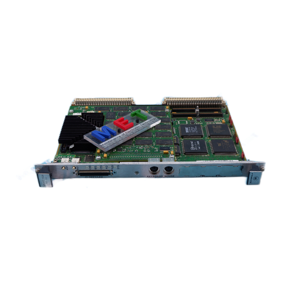
- Page 19 Overview The MVME2600 series SBC family, hereafter sometimes referred to simply as the MVME2600 or the V2600 series, provides many standard features required by a computer system: SCSI, Ethernet interface, keyboard interface, mouse interface, sync and async serial ports, parallel port, boot Flash, and up to 256MB of ECC DRAM.
- Page 20 RESET/ABORT Switch Status LEDs System Block Diagram The MVME2600 series provides the 256KB look-aside external cache option. The Falcon chip set controls the boot Flash and the ECC DRAM. The Raven ASIC functions as the 64-bit PCI host bridge and the MPIC interrupt controller. PCI devices include: SCSI, VME, Ethernet, and one PMC slot.
Need help?
Do you have a question about the MVME2600 Series and is the answer not in the manual?
Questions and answers