
Related Manuals for Advantech PCIE-1750U


Summary of Contents for Advantech PCIE-1750U
- Page 1 User Manual PCIE-1750U/UH 32-ch Isolated Digital I/O with Digital Filter PCI Express Card...
- Page 2 No part of this manual may be reproduced, copied, translated or transmitted in any form or by any means without the prior written permission of Advantech Co., Ltd. Information provided in this manual is intended to be accurate and reliable. How- ever, Advantech Co., Ltd.
- Page 3 Consult the dealer or an experienced radio/TV technician for help. Technical Support and Assistance Visit the Advantech web site at www.advantech.com/support where you can find the latest information about the product. Contact your distributor, sales representative, or Advantech's customer service center for technical support if you need additional assistance.
- Page 4 DO NOT LEAVE THIS EQUIPMENT IN AN ENVIRONMENT WHERE THE STORAGE TEMPERATURE MAY GO BELOW -20° C (-4° F) OR ABOVE 60° C (140° F). THIS COULD DAMAGE THE EQUIPMENT. THE EQUIPMENT SHOULD BE IN A CONTROLLED ENVIRONMENT. PCIE-1750U/UH User Manual...
- Page 5 70 dB (A). Safety Precaution - Static Electricity DISCLAIMER: This set of instructions is given according to IEC 704-1. Advantech disclaims all responsibility for the accuracy of any statements contained herein. Follow these simple precautions to protect yourself from harm and the products from damage.
- Page 6 PCIE-1750U/UH User Manual...
-
Page 7: Table Of Contents
Signal Connections ......9 Overview ....................10 Switch and Jumper Settings..............10 Figure 3.1 Card layout of PCIE-1750U/UH........ 10 Table 3.1: Summary of Jumper Settings (JP2)......10 Table 3.2: Board ID setting (SW1)..........11 Signal Connections ................. 12 Figure 3.2 Pin assignment of PCIE-1750U/UH......12 Figure 3.3 Isolated DI Connection .......... - Page 8 PCIE-1750U/UH User Manual viii...
-
Page 9: Chapter 1 Overview
Chapter Overview... -
Page 10: Introduction
, the PCIE-1750U/UH can still manage to work prop- erly, albeit only for a short period of time. Wide Input Range The PCIE-1750U/UH has a wide range of input voltage from 10 to 30 V , and is suitable for most industrial applications of 12 V or 24 V input voltage. -
Page 11: Applications
Board ID The PCIE-1750U/UH has a built-in DIP Switch that helps define each card’s ID when multiple PCIE-1750U/UH cards have been installed on the same PC chassis. The board ID setting function is very useful when users build a system with multiple PCIE- 1750U/UH cards. -
Page 12: Software Overview
Software Overview Advantech offers device drivers, SDKs, third-party driver support and application software to help fully exploit the functions of your PCIE-1750U/UH card. All these software packages are available on Advantech website: http://www.advantech.com/. Accessories Advantech offers a complete set of accessory products to support the PCIE-1750U/ UH card. -
Page 13: Chapter 2 Hardware Installation
Chapter Hardware Installation... -
Page 14: Installation
This chapter gives users a package item checklist, proper instructions about unpack- ing and step-by-step procedures for both driver and card installation. Unpacking After receiving your PCIE-1750U/UH package, please inspect the contents. The package should contain the following items: ... -
Page 15: Driver Installation
Touch the metal part on the surface of your computer to neutralize the static electricity that might be on your body. Insert the PCIE-1750U/UH card into a PCI Express slot. Hold the card only by its edges and carefully align it with the slot. Insert the card firmly into place. Use of excessive force must be avoided, otherwise the card might be damaged. -
Page 16: Figure 2.1 Device Manager
After the PCIE-1750U/UH card is installed, you can verify whether it is properly installed on your system through the Device Manager: Access the Device Manager through Control Panel/System/Device Manager. The device name of the PCIE-1750U/UH should be listed on the Device Man- ager tab as follows. -
Page 17: Chapter 3 Signal Connections
Chapter Signal Connections... -
Page 18: Overview
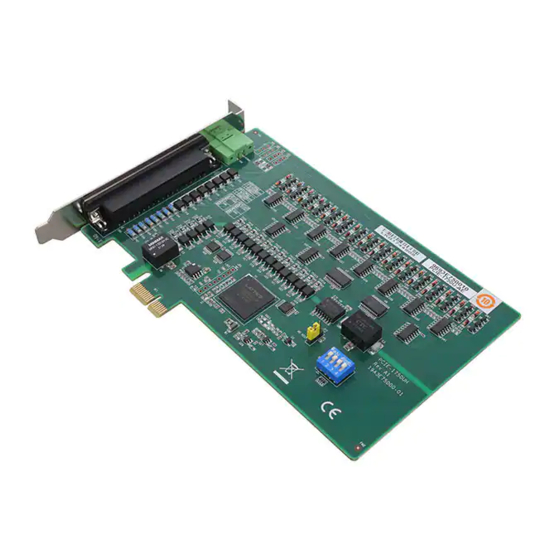
PC and other hardware devices. This chapter provides useful information about how to connect input and output signals to the PCIE-1750U/UH via the I/O connector. Switch and Jumper Settings Figure 3.1 Card layout of PCIE-1750U/UH Table 3.1: Summary of Jumper Settings (JP2) -
Page 19: Table 3.2: Board Id Setting (Sw1)
Table 3.2: Board ID setting (SW1) Board ID * Default Note! On: 1, Off: 0; Default setting: ID0. PCIE-1750U/UH User Manual... -
Page 20: Signal Connections
Signal Connections Figure 3.2 Pin assignment of PCIE-1750U/UH PCIE-1750U/UH User Manual... -
Page 21: Figure 3.3 Isolated Di Connection
Figure 3.3 Isolated DI Connection Isolated Digital Output The PCIE-1750U/UH provides software configurable digital output direction that allows users to choose from NPN or PNP. Whenever the direction is set to NPN and connect the wiring like Fig 3.4, the current will sink into the IDO channel as the IDO channel is switched HIGH. -
Page 22: Figure 3.5 Source Type (Pnp) Connection
The output type mismatch between software setting and wiring wouldn’t make any damage to the card itself. The only thing would happen is no reaction. Figure 3.6 describes the way mismatching makes no harm to the card itself. Figure 3.6 Wrong connection wouldn’t damage the IDO component PCIE-1750U/UH User Manual... -
Page 23: Figure 3.7 Pin Definition Of Cn2
CN2 provides two extra connections which are equivalent to the GND/PCOM pin on CN1. It brings extra current tolerance to PCIE-1750U/UH. The pin on CN2 should be connected whenever the total current of IDO is higher than 3.2A. The Pin assign- ment: Pin 1: PCOM, used in source type (PNP) connection. - Page 24 PCIE-1750U/UH User Manual...
-
Page 25: Appendix A Specifications
Appendix Specifications... -
Page 26: Specifications
Logic 0: 3 V max. (0 V min.) Input Voltage Logic 1: 10 V min. (30 V max.) 3.4mA @12V Input Current 7.13mA @24V PCIE-1750U: 2 (Ch0, 8) Interrupt Capable Ch. PCIE-1750UH: 16 Digital Filter Ch. 16 (PCIE-1750UH only) 2,500 V Isolation Protection 70 V... -
Page 27: General
2.048msec 8 (08h) 32μsec 15 (0Fh) 4.096msec 9 (09h) 64μsec 16 (10h) 8.192msec 10 (0Ah) 128μsec 17 (11h) 16.384msec 11 (0Bh) 256μsec 18 (12h) 32.768msec 12 (0Ch) 512μsec 19 (13h) 65.536msec 13 (0Dh) 1.024msec 20 (14h) 131.072msec PCIE-1750U/UH User Manual... - Page 28 PCIE-1750U/UH User Manual...
-
Page 29: Appendix B Block Diagram
Appendix Block Diagram... -
Page 30: Pcie-1750U/Uh
PCIE-1750U/UH PCIE-1750U/UH User Manual... - Page 31 PCIE-1750U/UH User Manual...
- Page 32 No part of this publication may be reproduced in any form or by any means, electronic, photocopying, recording or otherwise, without prior written permis- sion of the publisher. All brand and product names are trademarks or registered trademarks of their respective companies. © Advantech Co., Ltd. 2019...
Need help?
Do you have a question about the PCIE-1750U and is the answer not in the manual?
Questions and answers