
Related Manuals for Advantech PCIE-1762H


Summary of Contents for Advantech PCIE-1762H
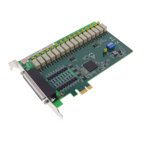
- Page 1 User Manual PCIE-1762H 16-Channel Relay and 16- Channel Isolated Digital Input PCIe Card...
- Page 2 No part of this manual may be reproduced, copied, translated, or transmitted in any form or by any means without the prior written permission of Advantech Co., Ltd. The information provided in this manual is intended to be accurate and reliable.
- Page 3 CE-compliant industrial enclosure prod- ucts. Technical Support and Assistance Visit the Advantech website at www.advantech.com/support to obtain the latest product information. Contact your distributor, sales representative, or Advantech's customer service center for technical support if you need additional assistance. Please have the following information ready before calling: –...
- Page 4 In accordance with IEC 704-1:1982 specifications, the sound pressure level at the operator’s position does not exceed 70 dB (A). DISCLAIMER: These instructions are provided according to IEC 704-1 standards. Advantech disclaims all responsibility for the accuracy of any statements contained herein. PCIE-1762H User Manual...
-
Page 5: Table Of Contents
Table 2.1: Summary of Jumper Settings ........7 Table 2.2: Board ID Settings (SW1) ..........7 Table 2.3: Jumper Settings for Relay .......... 8 I/O Connectors ..................9 Figure 2.2 I/O Connector Pin Assignments for PCIE-1762H ..9 Chapter Signal Connections ......11 Overview .................... - Page 6 PCIE-1762H User Manual...
-
Page 7: Chapter 1 Overview
Chapter Overview... -
Page 8: Introduction
Board ID The PCIE-1762H features a built-in DIP switch for defining the ID of each card. This is particularly useful for when multiple PCIE-1762H cards are installed on the same PC chassis. With the Board ID function, users can easily identify and access each card during hardware configuration and software programming operations. -
Page 9: Applications
Reset Protection for Industrial Applications When the system has undergone a hot reset, the PCIE-1762H card can either retain the output values for each channel or return to the default open configuration depending on the on-board jumper settings. This protects the system from malfunc- tioning during unexpected system resets. -
Page 10: Accessories
“twisted-pair cable”, reducing cross-talk and noise from other signal sources. Further- more, the analog and digital lines are separately sheathed and shielded to avoid EMI/ EMC problems. Advantech provides 1 m, 3 m, and 5 m cables to satisfy various usage requirements. -
Page 11: Chapter 2 Installation
Chapter Installation... -
Page 12: Unpacking
1 x PCIE-1762H startup manual Switch and Jumper Settings The PCIE-1762H card is equipped with one function switch and two jumper settings. Information regarding how to configure the card is provided below. Additionally, Fig- ure 2.1 shows the connector, jumper, switch locations to enable users to identify card components. -
Page 13: Table 2.1: Summary Of Jumper Settings
Default configuration Board ID (SW1) The PCIE-1762H card features a built-in DIP switch (SW1) that is used to define each card’s board ID. When multiple cards are installed on the same chassis, the board ID switch is useful for identifying each card by its device number. -
Page 14: Table 2.3: Jumper Settings For Relay
A complete loss of power to the chip will clear the chip memory. Therefore, regard- less of how JP2 is configured, if the power to the PCIE-1762H card is disconnected, the relay initial power-on state will be “OFF” (NC or NO, depending on the user’s set- tings). -
Page 15: I/O Connectors
External common input of Group 3 - NC: No connection - RLY_OUT n(n= 0 ~ 15): Relay output channel - RLY_COM n(n= 0 ~ 15): Relay output common channel Figure 2.2 I/O Connector Pin Assignments for PCIE-1762H PCIE-1762H User Manual... - Page 16 PCIE-1762H User Manual...
-
Page 17: Chapter 3 Signal Connections
Chapter Signal Connections... -
Page 18: Overview
Good signal connections can avoid unnecessary and costly damage to your PC and other hardware devices. This chapter explains how to connect input and output signals to the PCIE-1762H card via the I/O connector. -
Page 19: Relay Connections
Relay Connections After power on, the initial relay output status of the PCIE-1762H card should be as shown in Figure 3.2 below. Figure 3.2 Relay Output Connections A write operation to I/O address, BASE +0, will change the output status of each relay. - Page 20 PCIE-1762H User Manual...
-
Page 21: Appendix A Specifications
Appendix Specifications... -
Page 22: Isolated Digital Inputs
16.384 msec 4 (04h) 2 μsec 11 (0Bh) 256 μsec 18 (12h) 32.768 msec 5 (05h) 4 μsec 12 (0Ch) 512 μsec 19 (13h) 65.536 msec 6 (06h) 8 μsec 13 (0Dh) 1.024 msec 20 (14h) 131.072 msec PCIE-1762H User Manual... -
Page 23: Relay Outputs
+3.3 V @ 0.5 A (typical) +3.3 V @ 0.7 A (max.) Temperature Operating 0 ~ 60 °C (32 ~ 140 °F) Storage -20 ~ 70 °C (-4 ~ 158 °F) Relative Humidity 10 - 95% RH non-condensing Certifications CE/FCC PCIE-1762H User Manual... - Page 24 PCIE-1762H User Manual...
-
Page 25: Appendix B Block Diagram
Appendix Block Diagram... -
Page 26: Block Diagram
Block Diagram Appendix PCIE-1762H User Manual... - Page 27 PCIE-1762H User Manual...
- Page 28 No part of this publication may be reproduced in any form or by any means, such as electronically, by photocopying, recording, or otherwise, without prior written permission from the publisher. All brand and product names are trademarks or registered trademarks of their respective companies. © Advantech Co., Ltd. 2018...
Need help?
Do you have a question about the PCIE-1762H and is the answer not in the manual?
Questions and answers