Table of Contents
Advertisement
Quick Links
Advertisement
Table of Contents

Related Manuals for Advantech PCIE-1805


Summary of Contents for Advantech PCIE-1805
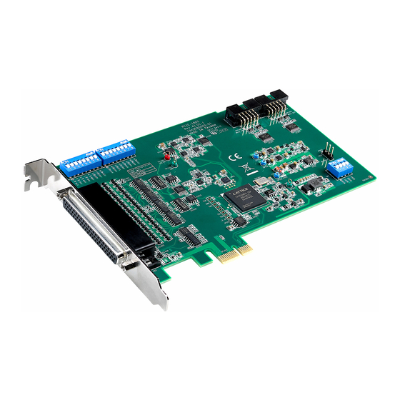
- Page 1 User Manual PCIE-1805 32-ch, 16-bit, 1 MS/s Analog Input PCI Express Card...
- Page 2 Because of Advantech’s high quality-control standards and rigorous testing, most of our customers never need to use our repair service. If an Advantech product is defec- tive, it will be repaired or replaced at no charge during the warranty period. For out- of-warranty repairs, you will be billed according to the cost of replacement materials, service time and freight.
- Page 3 This product has passed the CE test for environmental specifications when shielded cables are used for external wiring. We recommend the use of shielded cables. This kind of cable is available from Advantech. Please contact your local supplier for ordering information.
- Page 4 PCIE-1805 User Manual...
-
Page 5: Table Of Contents
Device Auto Installation (Recommended)........8 Device Setup & Configuration ..............9 Figure 2.1 The Device Setting of PCIE-1805....... 9 Figure 2.2 The Device Setting page .......... 10 Figure 2.3 The Device Testing of PCIE-1805 ......11 Chapter Signal Connections ......13 Overview .................... - Page 6 Analog Input Ranges and Gains..........30 B.1.3 AI Trigger Modes ................ 31 B.1.4 AI CONV Clock Source............... 33 B.1.5 AI Trigger Source................ 34 Table B.1: Analog Input Data Format ........34 Table B.2: Full Scale Values for Input Voltage Ranges..... 34 PCIE-1805 User Manual...
-
Page 7: Chapter 1 Introduction
Chapter Introduction This chapter introduces PCIE- 1805 and its typical applications. Sections include: Features Applications Installation Guide Software Overview Roadmap Accessories ... -
Page 8: Features
PCIE-1805 is an advanced high-performance analog input card based on the PCIe x1 Bus. With a large FIFO of 4K samples, the maximum sampling rate of PCIE-1805 is up to 1MkS/s shared by maximum 32 channels. Features 32-ch single-ended or 16-ch differential analog input, up to 1MS/s ... -
Page 9: Applications
Transducer and sensor measurements Waveform acquisition and analysis Vibration and transient analysis Installation Guide Before you install your PCIE-1805 card, please make sure you have the following necessary components: PCIE-1805 DA&C card PCIE-1805 User Manual ... - Page 10 Figure 1.1 Installation Flow Chart PCIE-1805 User Manual...
-
Page 11: Software Overview
Software Overview Advantech offers a rich set of DLL drivers, third-party driver support, and application software to help fully exploit the functions of your PCIE-1805 card: Device Drivers (downloaded from Advantech website) LabVIEW driver Advantech DAQNavi ... -
Page 12: Accessories
Advantech Navigator. Programming with DAQNavi Device Drivers Function Library Advantech DAQNavi Device Drivers offer a rich function library that can be utilized in various application programs. This function library consists of numerous APIs that support many development tools, such as Visual Studio .NET, Visual C++, Visual Basic, Delphi and C++ Builder. -
Page 13: Chapter 2 Installation
Chapter Installation... -
Page 14: Unpacking
2.2.1 Device Auto Installation (Recommended) You can install the PCIE-1805 in any PCI Express slot on your computer. Follow the steps below to install the module on your system. Turn off your computer and unplug the power cord and cables. TURN OFF your computer before installing or removing any components on the computer. -
Page 15: Device Setup & Configuration
APIs of Advantech Device Drivers. Setting Up the Device To set up the I/O device for your card, you must first run the Advantech Naviga- tor program (by accessing Start/Programs/Advantech Automation/DAQNavi/ Advantech Navigator). - Page 16 Configuring the Device Go to the Device Setting to configure your device. Here you can configure not only the Analog Input of PCIE-1805 but also Digital Input/Output. Figure 2.2 The Device Setting page PCIE-1805 User Manual...
- Page 17 After your card is properly installed and configured, you can go to the Device Test page to test your hardware by using the testing utility supplied. Figure 2.3 The Device Testing of PCIE-1805 For more detailed information, refer to the DAQNavi SDK Manual or the User Inter- face Manual in the Advantech Navigator.
- Page 18 PCIE-1805 User Manual...
-
Page 19: Chapter 3 Signal Connections
Chapter Signal Connections This chapter provides useful information about how to connect input and output signals to the PCIE-1805 card via the I/O con- nector. Sections include: Overview Board ID Settings Signal Connections Field Wiring Considerations... -
Page 20: Overview
This chapter provides useful information about how to connect input and output signals to the PCIE-1805 card via the I/O connector. Switch and Jumper Settings Please refer to Figure 3.1 for jumper and switch locations on PCIE-1805. Figure 3.1 Connector and Switch Locations PCIE-1805 User Manual... -
Page 21: Board Id (Sw1)
3.2.1 Board ID (SW1) The PCIE-1805 has a built-in DIP switch (SW1), which is used to define each card’s board ID. When there are multiple cards on the same chassis, this board ID switch is used to set each card’s device number. -
Page 22: Signal Connections
Signal Connections Pin Assignments The I/O connector on the PCIE-1805 is a 62-pin connector that allows you to connect to accessories with the PCL-10162 shielded cable. Figure 3.2 shows the pin assignments for the 62-pin I/O connector on the PCIE-1805, and Table 3.3 shows its I/O connector signal description. -
Page 23: I/O Connector Signal Description
External conversion clock input Power and Ground +12V +12 V power supply for external use +5 V power supply for external use AGND 47 ~ 63 Ground for analog signals DGND 43 ~ 46 Ground for digital signals RESERVED PCIE-1805 User Manual... -
Page 24: Measurement Mode Selection
PCIE-1805. With this connection, the PGIA rejects a common-mode voltage Vcm between the signal source and the PCIE-1805 ground, shown as Vcm in Figure 3-4. PCIE-1805 User Manual... - Page 25 Figure 3-4 shows a differential channel connection between a floating signal source and an input channel on the PCIE-1805. In this figure, each side of the floating signal source is connected through a resistor to the AGND. This connection can reject the common-mode voltage between the signal source and the PCIE-1805 ground Figure 3.4 Differential Input Channel Connection - Floating Signal Source...
- Page 26 20 kHz signal, you have to specify a sampling frequency of at least 40 kHz. This consideration can avoid an error condition often know as aliasing, in which high frequency input components appear erroneously as lower frequencies when sampling. PCIE-1805 User Manual...
- Page 27 1805 detects either a rising or falling edge on the External AI TTL trigger input signal from screw terminal DTRG0 and DTRG1 on the screw terminal board. The trigger signal is TTL-compatible. Figure 3.6 External Digital Trigger Source Connection PCIE-1805 User Manual...
-
Page 28: Field Wiring Considerations
AI0 - AI31. Field Wiring Considerations When you use PCIE-1805 cards to acquire data from outside, noises in the environ- ment might significantly affect the accuracy of your measurements if due cautions are not taken. The following measures will be helpful to reduce possible interference run- ning signal wires between signal sources and the PCIE-1805 card. -
Page 29: Appendix A Specifications
Appendix Specifications... -
Page 30: Function Block
Function Block PCIE-1805 User Manual... -
Page 31: Analog Input
>1,000 GΩ in parallel with 9 pF A+ to A- >1,000 GΩ in parallel with 6 pF Input bias current 4,095 samples shared by all enabled Input FIFO size channels Data transfers DMA, programmed I/O Overvoltage protection for all channels ±15 V PCIE-1805 User Manual... -
Page 32: Voltage Measurement Accuracy
Delay range 1 ~ 16777216 samples A.3.1 Analog Trigger Channels Source Any analog input channel Threshold level Full scale of analog input range, software programmable Resolution 16 bits Hysteresis Software programmable Polarity Rising edge/falling edge, software selectable PCIE-1805 User Manual... -
Page 33: External Digital Trigger
62-pin D-sub × 1 Operating temperature 0 to 60 °C (32 to 140 °F) Storage temperature -40 to 70 °C (-40 to 158 °F) Operating humidity 10 to 90% RH, non-condensing Storage humidity 5 to 95% RH, non-condensing PCIE-1805 User Manual... - Page 34 PCIE-1805 User Manual...
-
Page 35: Operation Theory
Appendix Operation Theory... -
Page 36: Analog Input Operation
B.1.2 Analog Input Ranges and Gains The PCIE-1805 can measure both unipolar and bipolar analog input signals. A unipo- lar signal can range from 0 to 10 V FSR (Full Scale Range), while a bipolar signal extends within ±10 V FSR. The PCIE-1805 provides various programmable gain lev- els and each channel is allowed to set its own input range individually. -
Page 37: Ai Trigger Modes
B.1.3 AI Trigger Modes The PCIE-1805 supports four trigger modes and pause function. User can start or stop the operation by trigger mode selection. An extra 24-bit counter is dedicated to delay-trigger mode and about-trigger mode. Figure shows the four different trigger modes. - Page 38 CONV CLKs has been taken after the trigger event. User can set the delay number of CONV CLKs by a 24-bit counter. Delay to start trigger acquisition starts when the PCIE-1805 detects the trigger event and stops when you stop the operation.
-
Page 39: Ai Conv Clock Source
B.1.4 AI CONV Clock Source The PCIE-1805 can adopt both internal and external clock sources to accomplish pacer acquisition. You can set the clock and trigger sources conveniently by soft- ware. The figure can help you understand the routing route of clock and trigger gen- eration. -
Page 40: Ai Trigger Source
External digital (TTL) trigger Analog threshold trigger With PCIE-1805, user can also define the type of trigger source as rising-edge or fall- ing-edge. These following sections describe these trigger sources in more detail. External Digital (TTL) Trigger ... - Page 41 PCIE-1805 User Manual...
- Page 42 No part of this publication may be reproduced in any form or by any means, electronic, photocopying, recording or otherwise, without prior written permis- sion of the publisher. All brand and product names are trademarks or registered trademarks of their respective companies. © Advantech Co., Ltd. 2020...
Need help?
Do you have a question about the PCIE-1805 and is the answer not in the manual?
Questions and answers