Table of Contents
Advertisement
CMOS single-chip 8-bit MCU
with EEPROM and 12-bit A/D
converter
Main features
8-bit Microcontroller with high speed 8051 CPU
Basic MCU Function
– 8Kbytes Flash Code Memory
– 512bytes EEPROM Backup Memory
– 512bytes SRAM Data Memory
Built-in Analog Function
– Power-On Reset and Brown Out Detect Reset
– Internal 8MHz RC Oscillator (±3%, T
– Internal 1MHz RING Oscillator
Peripheral features
– 12-bit Analog to Digital Converter (15inputs)
– Serial Interface (USART + SPI + I2C)
– 6-channel 10-bit PWM for Motor Control
I/O and packages
– Up to 30 programmable I/O lines with 32SOP
– 32/28/20/16 SOP
Operating conditions
– 1.8V to 5.5V wide voltage range
– -40°C to 85°C temperature range
Application
– Small Home Appliance
– BLDC Motor Controller
– LED Lighting with High speed PWM
–
(7-bit duty 500kHz period ~ 10-bit duty 62.5kHz period)
= -40 ~ +85°C)
A
MC95FG308
MC95FG208
User's manual
V 3.4
Revised 12 May, 2015
Advertisement
Table of Contents

Subscribe to Our Youtube Channel
Related Manuals for Abov MC95FG208 Series


Summary of Contents for Abov MC95FG208 Series
- Page 1 CMOS single-chip 8-bit MCU with EEPROM and 12-bit A/D converter MC95FG308 Main features MC95FG208 8-bit Microcontroller with high speed 8051 CPU User’s manual Basic MCU Function – 8Kbytes Flash Code Memory V 3.4 – 512bytes EEPROM Backup Memory –...
-
Page 2: Revision History
The information, diagrams and other data in this manual are correct and reliable; however, ABOV Semiconductor is in no way responsible for any violations of patents or other rights of the third party generated by the use of this manual. -
Page 3: Overview
MC95FG308 / MC95FG208 ABOV Semiconductor Co., Ltd. Overview 1.1. Description The MC95FG308 is an advanced CMOS 8-bit microcontroller with 8Kbytes of FLASH. This is powerful microcontroller which provides a highly flexible and cost effective solution to many embedded control applications. This provides the... -
Page 4: Features
ABOV Semiconductor Co., Ltd. MC95FG308 / MC95FG208 Features – Analog Comparator (1) – 8-bit CISC core (8051 Compatible, 2 clock per cycle) – WDT (1) – WT (1) 8Kbytes On-Chip FLASH – BIT (1) – Optional boot code section with protection –... -
Page 5: Development Tools
1.3.1 Compiler ABOV Semiconductor does not provide compiler. It is recommended that you consult a compiler provider. The MC95FG308 core is Mentor 8051, and the ROM size is smaller than 64Kbytes.Therefore, developer can use the standard 8051 compiler from other providers. -
Page 6: Programmer
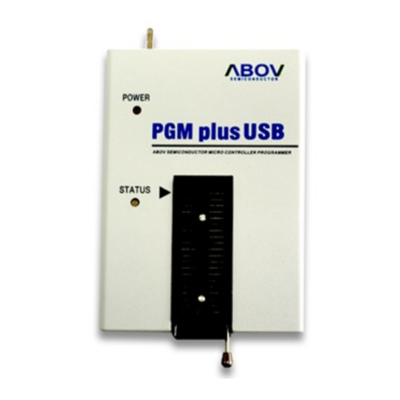
ABOV Semiconductor Co., Ltd. MC95FG308 / MC95FG208 1.3.3 Programmer Single programmer: PGMplus USB: It programs MCU device directly. Figure 1.2 PGMplusUSB(Single writer) Standalone PGMplus: It programs MCU device directly. Figure 1.3 Standalone PGMplus(Single writer) - Page 7 MC95FG308 / MC95FG208 ABOV Semiconductor Co., Ltd. Gang programmer: It programs 8 MCU devices at once.So, it is mainly used in mass production factory. Gang programmer is standalone type, it means it does not require host PC, after a program is downloaded from host PC to Gang programmer.
-
Page 8: Block Diagram
ABOV Semiconductor Co., Ltd. MC95FG308 / MC95FG208 Block diagram DSCL/P06 DSDA/P07 P25/AN14 P24/AN13 P23/AN12 On-Chip P37/AN11 P06~P00 PORT Debug P36/AN10 P16/AN9 P15/AN8 12-BIT P07/AN7 P16~P10 PORT M8051 P06/AN6 P05/AN5 CORE P04/AN4 P03/AN3 P26~P20 PORT P02/AN2 P01/AN1 EEPROM P00/AN0 (512B) (512B) -
Page 9: Pin Assignment
MC95FG308 / MC95FG208 ABOV Semiconductor Co., Ltd. Pin assignment (TxD0) / INT6 / P32 P31 / INT5 (RxD0) / INT7 / P33 P30 / INT4 SXIN / AC- / AN4 / P04 P03 / RxD0 / MISO0 / EC2 / AN3... - Page 10 ABOV Semiconductor Co., Ltd. MC95FG308 / MC95FG208 (DSCL)/ACOUT/AN6/T0O/SCL/P06 P01 / ACK0 / SCK0 / AN1 (DSDA) / AN7 / EC0 / SDA / P07 P00 / SS0 / AN0 / AVref AN14 / (SCL) / P25 P24 / AN13 MC95FG308U...
- Page 11 MC95FG308 / MC95FG208 ABOV Semiconductor Co., Ltd. (DSCL)/ACOUT/AN6/T0O/SCL/P06 P01 / ACK0 / SCK0 / AN1 (DSDA) / AN7 / EC0 / SDA / P07 P00 / SS0 / AN0 / AVref AN14 / (SCL) / P25 P24 / AN13 MC95FG308L...
- Page 12 ABOV Semiconductor Co., Ltd. MC95FG308 / MC95FG208 (TxD0) / INT6 / P32 P31 / INT5 (RxD0) / INT7 / P33 P30 / INT4 SXIN / AC- / AN4 / P04 P03 / RxD0 / MISO0 / EC2 / AN3 SXOUT / AC+ / AN5 / P05...
- Page 13 MC95FG308 / MC95FG208 ABOV Semiconductor Co., Ltd. SXIN / AC- / AN4 / P04 P03 / RxD0 / MISO0 / EC2 / AN3 SXOUT / AC+ / AN5 / P05 P02 / TxD0 / MOSI0 / T2O / AN2 (DSCL) / ACOUT / AN6 / T0O / SCL / P06...
-
Page 14: Package Diagram
ABOV Semiconductor Co., Ltd. MC95FG308 / MC95FG208 Package Diagram Figure 4.1 32-Pin SOP Package... - Page 15 MC95FG308 / MC95FG208 ABOV Semiconductor Co., Ltd. Figure 4.2 32-Pin QFN Package...
- Page 16 ABOV Semiconductor Co., Ltd. MC95FG308 / MC95FG208 Figure 4.3 32-Pin LQFP Package...
- Page 17 MC95FG308 / MC95FG208 ABOV Semiconductor Co., Ltd. Figure 4.4 28-Pin SOP Package...
- Page 18 ABOV Semiconductor Co., Ltd. MC95FG308 / MC95FG208 Figure 4.5 28-Pin SOP Package (continue)
- Page 19 MC95FG308 / MC95FG208 ABOV Semiconductor Co., Ltd. Figure 4.6 28-Pin SOP Package...
- Page 20 ABOV Semiconductor Co., Ltd. MC95FG308 / MC95FG208 Figure 4.7 28-Pin TSSOP Package...
- Page 21 MC95FG308 / MC95FG208 ABOV Semiconductor Co., Ltd. Figure 4.8 20-Pin SOP Package...
- Page 22 ABOV Semiconductor Co., Ltd. MC95FG308 / MC95FG208 Figure 4.9 20-Pin TSSOP Package...
- Page 23 MC95FG308 / MC95FG208 ABOV Semiconductor Co., Ltd. Figure 4.10 16-Pin SOP Package...
- Page 24 ABOV Semiconductor Co., Ltd. MC95FG308 / MC95FG208 Figure 4.11 16-Pin TSSOP Package...
-
Page 25: Pin Description
MC95FG308 / MC95FG208 ABOV Semiconductor Co., Ltd. Pin Description Function @RESET Shared with Name Port P0 Avref / AN0 / SS0 8-bit I/O Port AN1 / SCK0 / ACK0 Can be set in input or output mode in 1-bit units... -
Page 26: Port Structures
ABOV Semiconductor Co., Ltd. MC95FG308 / MC95FG208 Port Structures General Purpose I/O Port LevelShift ( 1.8V to ExtVDD) LevelShift (ExtVDD to 1.8V) PULL-UP REGISTER OPEN DRAIN REGISTER DATA REGISTER SUB-FUNC DATA OUTPUT SUB-FUNC ENABLE SUB-FUNC DIRECTION DIRECTION REGISTER R(400Ω) PORTx INPUT... -
Page 27: External Interrupt I/O Port
MC95FG308 / MC95FG208 ABOV Semiconductor Co., Ltd. External Interrupt I/O Port LevelShift ( 1.8V to ExtVDD) LevelShift (ExtVDD to 1.8V) PULL-UP REGISTER OPEN DRAIN REGISTER DATA REGISTER SUB-FUNC DATA OUTPUT SUB-FUNC ENABLE SUB-FUNC DIRECTION DIRECTION REGISTER R(400Ω) EXTERNAL INTERRUPT POLARITY... -
Page 28: Electrical Characteristics
ABOV Semiconductor Co., Ltd. MC95FG308 / MC95FG208 Electrical Characteristics Absolute Maximum Ratings Parameter Symbol Rating Unit -0.3~+6.5 Supply Voltage -0.3~+0.3 -0.3~VDD+0.3 -0.3~VDD+0.3 Normal Voltage Pin ∑ ∑ Total Power Dissipation ℃ Storage Temperature TSTG -65~+150 Absolute Maximum Ratings Table 7.1 NOTE) Stresses beyond those listed under “Absolute Maximum Ratings”... -
Page 29: A/D Converter Characteristics
MC95FG308 / MC95FG208 ABOV Semiconductor Co., Ltd. A/D Converter Characteristics (TA=-40℃ ~ +85℃, VDD=AVDD=2.7V ~ 5.5V, VSS=0V) Parameter Symbol Condition Unit A/D converting Resolution bits Integral Linearity Error ±3 Differential Linearity Error ±2 Vref=5.12V, Offset Error of Top -±1 ±3 Vss=0V, TA=+25℃... -
Page 30: Voltage Dropout Converter Characteristics
ABOV Semiconductor Co., Ltd. MC95FG308 / MC95FG208 Voltage Dropout Converter Characteristics Parameter Symbol Condition Unit Operating Voltage ℃ Operating Temperature Regulation Voltage 1.62 1.98 Drop-out Voltage 0.02 RUN/IDLE SUB-ACTIVE Current Drivability STOP1 STOP2 IDD1 RUN/IDLE IDD2 SUB-ACTIVE Operating Current SIDD1... -
Page 31: Internal Rc Oscillator Characteristics
MC95FG308 / MC95FG208 ABOV Semiconductor Co., Ltd. Internal RC Oscillator Characteristics Parameter Symbol Condition Unit Operating Voltage ℃ Operating Temperature Frequency 7.76 8.24 Stabilization Time Operating Current SIDD Internal RC Oscillator Characteristics Table 7.8 Ring-Oscillator Characteristics Parameter Symbol Condition Unit Operating Voltage ℃... -
Page 32: Dc Characteristics
ABOV Semiconductor Co., Ltd. MC95FG308 / MC95FG208 7.11 DC Characteristics (VDD =2.7~5.5V, VSS =0V, fXIN=10.0MHz, TA=-40~+85℃) Parameter Symbol Condition Unit VIL1 P2[2] -0.5 0.2VDD Input Low Voltage VIL2 All others PAD -0.5 0.2VDD VIH1 P2[2] 0.8VDD Input High Voltage VIH2 All others PAD 0.7VDD... -
Page 33: Ac Characteristics
MC95FG308 / MC95FG208 ABOV Semiconductor Co., Ltd. 7.12 AC Characteristics (VDD=5.0V±10%, VSS=0V, TA=-40~+85℃) Parameter Symbol Unit Operating Frequency fMCP System Clock Cycle Time tSYS 1000 Oscillation Stabilization Time (8MHz) tMST1 XIN, XOUT External Clock “H” or “L” Pulse Width tCPW... -
Page 34: Spi Characteristics
ABOV Semiconductor Co., Ltd. MC95FG308 / MC95FG208 7.13 SPI Characteristics (VDD=5.0V±10%, VSS=0V, TA=-40~+85℃) Parameter Symbol Unit Output Clock Pulse Period tSCK SPI clock mode Input Clock Pulse Period tSCK 2• tSYS Input Clock “H” or “L” Pulse Width tSCKL, tSCKH... -
Page 35: Main Clock Oscillator Characteristics
MC95FG308 / MC95FG208 ABOV Semiconductor Co., Ltd. 7.14 Main Clock Oscillator Characteristics (VDD=5.0V±10%, VSS=0V, TA=-40~+85℃) Parameter Operating Voltage (VDDEXT) 1.5V 5.5V TEMP -40℃ 85℃ 660uA @4Mhz, VDDEXT(+5V) Operating Frequency 12Mhz Ext. Load Cap 22pF 35pF C1,C2 Main Clock Oscillator Characteristics Table 7.14... -
Page 36: Typical Characteristics
ABOV Semiconductor Co., Ltd. MC95FG308 / MC95FG208 7.16 Typical Characteristics These graphs and tables provided in this section are for design guidance only and are not tested or guaranteed. In some graphs or tables the data presented are outside specified operating range (e.g. outside specified VDD range). -
Page 37: Memory
MC95FG308 / MC95FG208 ABOV Semiconductor Co., Ltd. Memory The MC95FG308 addresses two separate address memory stores: Program memory and Data memory. The logical separation of Program and Data memory allows Data memory to be assessed by 8-bit addresses, which can be more quickly stored and manipulated by 8-bit CPU. - Page 38 ABOV Semiconductor Co., Ltd. MC95FG308 / MC95FG208 FFFFH 1FFFH 8Kbytes 0000H Figure 8.1 Program Memory – User Function Mode: 8Kbytes Included Interrupt Vector Region – Non-volatile and reprogramming memory: Flash memory based on EEPROM cell...
-
Page 39: Data Memory
MC95FG308 / MC95FG208 ABOV Semiconductor Co., Ltd. Data Memory Figure 8.2 Data Memory Map The internal data memory space is divided into three blocks, which are generally referred to as the lower 128bytes, upper 128bytes, and SFR space. Internal data memory addresses are always one byte wide, which implies an address space of only 256bytes. - Page 40 ABOV Semiconductor Co., Ltd. MC95FG308 / MC95FG208 7F 7E 7D 7C 7B 7A 79 78 77 76 75 74 73 72 71 70 6F 6E 6D 6C 6B 6A 69 68 67 66 65 64 63 62 61 60 5F 5E 5D 5C 5B 5A 59 58...
-
Page 41: Eeprom Data Memory And Xsram
MC95FG308 / MC95FG208 ABOV Semiconductor Co., Ltd. EEPROM Data Memory and XSRAM MC95FG308 has 512bytes EEPROM Data memory. This area has no relation with RAM/FLASH. It can read and write through SFR with 8-bit unit. For more information about EEPROM Data memory, see chapter 15. -
Page 42: Sfr Map
ABOV Semiconductor Co., Ltd. MC95FG308 / MC95FG208 SFR Map 8.4.1 SFR Map Summary 0H/8H 1H/9H 2H/AH 3H/BH 4H/CH 5H/DH 6H/EH 7H/FH 2F58H FUSE_PKG FUSE_CAL2 FUSE_CAL1 FUSE_CAL0 FUSE_CONF TEST_REGB TEST_REGA 2F50H PSR0 PSR1 PSR2 2F48H 2F40H 2F38H 2F30H 2F28H 2F20H 2F18H... -
Page 43: 8051 Compiler Compatible Sfr
MC95FG308 / MC95FG208 ABOV Semiconductor Co., Ltd. 8.4.2 8051 Compiler Compatible SFR ACC (Accumulator) : E0H Initial value : 00H Accumulator B (B Register) : F0H Initial value : 00H B Register SP (Stack Pointer) : 81H Initial value : 07H... - Page 44 ABOV Semiconductor Co., Ltd. MC95FG308 / MC95FG208 PSW (Program Status Word) : D0H Initial value : 00H Carry Flag Auxiliary Carry Flag General Purpose User-Definable Flag Register Bank Select bit 1 Register Bank Select bit 0 Overflow Flag User-Definable Flag Parity Flag.
-
Page 45: O Ports
MC95FG308 / MC95FG208 ABOV Semiconductor Co., Ltd. I/O Ports I/O Ports The MC95FG308 has four I/O ports (P0, P1, P2 and P3). Each port can be easily configured by software as I/O pin, internal pull up and open drain pin to meet various system configurations and design requirements. Also P0 includes function that can generate interrupt according to change of state of the pin. -
Page 46: Port Selection Register (Psrx)
ABOV Semiconductor Co., Ltd. MC95FG308 / MC95FG208 9.2.6 Port Selection Register (PSRx) PSRx registers prevent the input leakage current when ports are connected to analog inputs. If the bit of PSRx is ‘1’, the dynamic current path of the schmitt OR gate of the port is cut off and the digital input of the corresponding port is always ‘1’. -
Page 47: Px Port
MC95FG308 / MC95FG208 ABOV Semiconductor Co., Ltd. Px Port 9.3.1 Px Port Description Px is 8-bit I/O port. Px control registers consist of Data register (Px), direction register (PxIO), debounce enable register (PxDB), pull-up register selection register (PxPU), open-drain selection register (PxOD), pin change interrupt register (PCI0). - Page 48 ABOV Semiconductor Co., Ltd. MC95FG308 / MC95FG208 PxDB (Px Debounce Enable Register) : 2F18H ~ 2F1BH Px7DB Px6DB Px5DB Px4DB Px3DB Px2DB Px1DB Px0DB Initial value : 00H PxDB[7:0] Configure debounce of Px port Disable Enable PCI0 (P0 Pin Change Interrupt Enable Register) : AEH...
-
Page 49: Port Reset Noise Canceller
MC95FG308 / MC95FG208 ABOV Semiconductor Co., Ltd. PSR2 (USART0, TIMER0 Port Selection Register) : 2F52H PSR20 Initial value : 00H PSR2[0] RxD0, TxD0, EC0, T0O ports selection register P0[3:2] for RxD0, TxD0 (default) P0[7:6] for EC0, T0O P3[3:2] for RxD0, TxD0... -
Page 50: Interrupt Controller
ABOV Semiconductor Co., Ltd. MC95FG308 / MC95FG208 Interrupt Controller 10.1 Overview The MC95FG308 supports up to 32 interrupt sources. The interrupts have separate enable register bits associated with them, allowing software control. They can also have four levels of priority assigned to them. The interrupt... -
Page 51: External Interrupt
MC95FG308 / MC95FG208 ABOV Semiconductor Co., Ltd. 10.2 External Interrupt The external interrupt on INT0, INT1, INT2, INT3, INT4, INT5, INT6 and INT7 pins receive various interrupt request depending on the EIEDGE (External Interrupt Edge register) and EIPOLA (External Interrupt Polarity register) and EIBOTH (External Interrupt Both Edge register) as shown in Figure 10.1. -
Page 52: Block Diagram
ABOV Semiconductor Co., Ltd. MC95FG308 / MC95FG208 10.3 Block Diagram EIEDGE[A5 IP0[B8 IP1[F8 EIPOLA[A6 IE0[A8 EIBOTH[A7 EIFLAG.0 [A4 FLAG0 INT0 Priority High EIFLAG.1 [A4 FLAG1 INT1 EIFLAG.2 [A4 INT2 FLAG2 EIFLAG.3 [A4 INT3 FLAG3 PCI(P0) INT5 IE1[A9 USTAT0.5[E5 UART0 Rx USTAT0.6[E6... -
Page 53: Interrupt Vector Table
MC95FG308 / MC95FG208 ABOV Semiconductor Co., Ltd. 10.4 Interrupt Vector Table The interrupt controller supports 32 interrupt sources as shown in the Table 10.2 below. When interrupt becomes service, long call instruction (LCALL) is executed in the vector address. Interrupt request 32 has a decided priority order. -
Page 54: Interrupt Sequence
ABOV Semiconductor Co., Ltd. MC95FG308 / MC95FG208 10.5 Interrupt Sequence An interrupt request is held until the interrupt is accepted or the interrupt latch is cleared to ‘0’ by a reset or an instruction. Interrupt acceptance always generates at last cycle of the instruction. So instead of fetching the current instruction, CPU executes internally LCALL instruction and saves the PC stack. -
Page 55: Effective Timing After Controlling Interrupt Bit
MC95FG308 / MC95FG208 ABOV Semiconductor Co., Ltd. 10.6 Effective Timing after Controlling Interrupt bit Interrupt Enable Register command Next Instruction Setting both EA bit and individual interrupt enable bit INTnE makes the pending interrupt active after executing the next instruction. -
Page 56: Interrupt Enable Accept Timing
ABOV Semiconductor Co., Ltd. MC95FG308 / MC95FG208 Example) Software Multi Interrupt: INT1: MOV IE, #01H ; Enable INT0 only IE1, #00H ; Disable others SETB ; Enable global interrupt (necessary for multi interrupt) IE, #0FFH ; Enable all Interrupts IE1, #0FFH RETI 10.8... -
Page 57: Saving/Restore General-Purpose Registers
MC95FG308 / MC95FG208 ABOV Semiconductor Co., Ltd. 10.10 Saving/Restore General-Purpose Registers INTxx : PUSH PSW PUSH DPL Main Task PUSH DPH Interrupt PUSH B Service Task PUSH ACC ∙ Saving ∙ Register Interrupt_Processing: ∙ Restoring POP ACC Register POP B... -
Page 58: Interrupt Register Overview
ABOV Semiconductor Co., Ltd. MC95FG308 / MC95FG208 NOTE) command cycle CLPx: L=Last cycle, 1=1 cycle or 1 phase, 2=2 cycle or 2 phase 10.12 Interrupt Register Overview 10.12.1 Interrupt Enable Register (IE, IE1, IE2, IE3, IE4, IE5) Interrupt enable register consists of Global interrupt control bit (EA) and peripheral interrupt control bits. Totally 32 peripheral are able to control interrupt. -
Page 59: Register Map
MC95FG308 / MC95FG208 ABOV Semiconductor Co., Ltd. 10.12.8 Register Map Name Address Default Description Interrupt Enable Register Interrupt Enable Register 1 Interrupt Enable Register 2 Interrupt Enable Register 3 Interrupt Enable Register 4 Interrupt Enable Register 5 Interrupt Priority Register... -
Page 60: Register Description For Interrupt
ABOV Semiconductor Co., Ltd. MC95FG308 / MC95FG208 10.13.1 Register Description for Interrupt IE (Interrupt Enable Register) : A8H INT5E INT4E INT3E INT2E INT1E INT0E Initial value : 00H Enable or disable all interrupt bits All Interrupt disable All Interrupt enable... - Page 61 MC95FG308 / MC95FG208 ABOV Semiconductor Co., Ltd. IE1 (Interrupt Enable Register 1) : A9H INT11E INT10E INT9E INT8E INT7E INT6E Initial value : 00H INT11E Enable or disable USART1 Tx Interrupt Disable Enable INT10E Enable or disable USART1 Rx Interrupt...
- Page 62 ABOV Semiconductor Co., Ltd. MC95FG308 / MC95FG208 IE3 (Interrupt Enable Register 3) : ABH INT23E INT22E INT21E INT20E INT19E INT18E Initial value : 00H INT23E Reserved Disable Enable INT22E Enable or disable BIT Interrupt Disable Enable INT21E Enable or disable WDT Interrupt...
- Page 63 MC95FG308 / MC95FG208 ABOV Semiconductor Co., Ltd. IE5 (Interrupt Enable Register 5) : ADH INT35E INT34E INT33E INT32E INT31E INT30E Initial value : 00H INT35E Reserved Disable Enable INT34E Reserved Disable Enable INT33E Reserved Disable Enable INT32E Reserved Disable Enable...
- Page 64 ABOV Semiconductor Co., Ltd. MC95FG308 / MC95FG208 EIFLAG (External Interrupt Flag Register) : A4H FLAG7 FLAG6 FLAG5 FLAG4 FLAG3 FLAG2 FLAG1 FLAG0 Initial value : 00H FLAG[7:0] If External Interrupt is occurred, the flag becomes ‘1’. The flag can be cleared by writing a ‘0’ to bit...
- Page 65 MC95FG308 / MC95FG208 ABOV Semiconductor Co., Ltd. EIBOTH (External Interrupt Both Edge Enable Register) : A7H BOTH7 BOTH 6 BOTH 5 BOTH 4 BOTH 3 BOTH 2 BOTH 1 BOTH 0 Initial value : 00H BOTH[7:0] Determines which type of interrupt may occur, EIBOTH or EIEDGE+EIPOLA.
-
Page 66: Peripheral Hardware
ABOV Semiconductor Co., Ltd. MC95FG308 / MC95FG208 Peripheral Hardware 11.1 Clock Generator 11.1.1 Overview As shown in Figure 11.1, the clock generator produces the basic clock pulses which provide the system clock to be supplied to the CPU and the peripheral hardware. It contains main-frequency clock oscillator. The system clock operation can be easily obtained by attaching a crystal between the XIN and XOUT pin, respectively. -
Page 67: Register Map
MC95FG308 / MC95FG208 ABOV Semiconductor Co., Ltd. 11.1.3 Register Map Name Address Default Description SCCR System and Clock Control Register Register Map Table 11.1 11.1.4 Clock Generator Register Description The Clock Generation Register uses clock control for system operation. The clock generation consists of System and Clock register. - Page 68 ABOV Semiconductor Co., Ltd. MC95FG308 / MC95FG208 fINTRC INTRC (8MHz) fXIN Main Clock (1~16MHz) fSUB (32.768kHz) fRING (125kHz)
-
Page 69: Basic Interval Timer
MC95FG308 / MC95FG208 ABOV Semiconductor Co., Ltd. 11.2 Basic Interval Timer 11.2.1 Overview The MC95FG308 has one 8-bit Basic Interval Timer that is free-run and can’t stop. Block diagram is shown in Figure 11.2. In addition, the Basic Interval Timer generates the time base for watchdog timer counting. It also provides a basic interval timer interrupt (BITF). -
Page 70: Basic Interval Timer Register Description
ABOV Semiconductor Co., Ltd. MC95FG308 / MC95FG208 11.2.4 Basic Interval Timer Register Description The Basic Interval Timer Register consists of Basic Clock control register (BCCR) and Basic Interval Timer register (BITR). If BCLR bit set to ‘1’, BITR becomes ‘0’ and then counts up. After 1 machine cycle, BCLR bit is cleared as ‘0’... -
Page 71: Watch Dog Timer
MC95FG308 / MC95FG208 ABOV Semiconductor Co., Ltd. 11.3 Watch Dog Timer 11.3.1 Overview The watchdog timer rapidly detects the CPU malfunction such as endless looping caused by noise or the like, and resumes the CPU to the normal state. The watchdog timer signal for detecting malfunction can be selected either a reset CPU or an interrupt request. -
Page 72: Watch Dog Timer Register Description
ABOV Semiconductor Co., Ltd. MC95FG308 / MC95FG208 11.3.4 Watch Dog Timer Register Description The Watch dog timer (WDT) Register consists of Watch Dog Timer Register (WDTR), Watch Dog Timer Counter Register (WDTCR) and Watch Dog Timer Mode Register (WDTMR). 11.3.5 Register Description for Watch Dog Timer... -
Page 73: Wdt Interrupt Timing Waveform
MC95FG308 / MC95FG208 ABOV Semiconductor Co., Ltd. 11.3.6 WDT Interrupt Timing Waveform Source Clock BIT Overflow WDTCR[7:0] Counter Clear WDTR[7:0] WDTCL Occur Match WDTIF WDTR 0000_0011b Detect Interrupt WDTRESETB RESET Figure 11.4 WDT Interrupt Timing Waveform... -
Page 74: Watch Timer
ABOV Semiconductor Co., Ltd. MC95FG308 / MC95FG208 11.4 Watch Timer 11.4.1 Overview The watch timer has the function for RTC (Real Time Clock) operation. It is generally used for RTC design. The internal structure of the watch timer consists of the clock source select circuit, timer counter circuit, output select circuit and watch timer mode register. -
Page 75: Watch Timer Register Description
MC95FG308 / MC95FG208 ABOV Semiconductor Co., Ltd. 11.4.4 Watch Timer Register Description The watch timer register (WT) consists of Watch Timer Mode Register (WTMR), Watch Timer Counter Register (WTCR) and Watch Timer Register (WTR). As WTMR is 6-bit writable/readable register, WTMR can control the clock source (WTCK), interrupt interval (WTIN) and function enable/disable (WTEN). - Page 76 ABOV Semiconductor Co., Ltd. MC95FG308 / MC95FG208 WTR (Watch Timer Register: Write Case) : 9EH WTCL WTR6 WTR5 WTR4 WTR3 WTR2 WTR1 WTR0 Initial value : 7FH WTCL Clear WT Counter Free Run Clear WT Counter (auto clear after 1 Cycle)
-
Page 77: Timer/Pwm
MC95FG308 / MC95FG208 ABOV Semiconductor Co., Ltd. 11.5 Timer/PWM 11.5.1 8-bit Timer/Event Counter 0, 1 Overview 11.5.1.1 Timer 0 and timer 1 can be used either two 8-bit timer/counter or one 16-bit timer/counter with combine them. Each 8- bit timer/event counter module has multiplexer, 8-bit timer data register, 8-bit counter register, mode register, input capture register, comparator. -
Page 78: 8-Bit Timer/Counter Mode
ABOV Semiconductor Co., Ltd. MC95FG308 / MC95FG208 8-bit Timer/Counter Mode 11.5.1.2 The 8-bit Timer/Counter Mode is selected by control registers as shown in Figure 11.6. ADDRESS : B2 T0EN T0PE CAP0 T0CK2 T0CK1 T0CK0 T0CN T0ST T0CR INITIAL VALUE : 0000_0000... - Page 79 MC95FG308 / MC95FG208 ABOV Semiconductor Co., Ltd. Match with T0DR/T1DR T0DR/T1DR Value Count Pulse Period Up-count TIME Interrupt Period x (n+1) Timer 0, 1 (T0IF, T1IF) Interrupt Occur Occur Occur Interrupt Interrupt Interrupt Figure 11.7 Timer/Event Counter 0, 1 Example...
-
Page 80: 16-Bit Timer/Counter Mode
ABOV Semiconductor Co., Ltd. MC95FG308 / MC95FG208 16-bit Timer/Counter Mode 11.5.1.3 The timer register is being run with all 16 bits. A 16-bit timer/counter register T0, T1 are incremented from 0003H to FFFFH until it matches T0DR, T1DR and then resets to 0000H. The match output generates the Timer 0 interrupt (No timer 1 interrupt). - Page 81 MC95FG308 / MC95FG208 ABOV Semiconductor Co., Ltd. ADDRESS : B2 T0EN T0PE CAP0 T0CK2 T0CK1 T0CK0 T0CN T0ST T0CR INITIAL VALUE : 0000_0000 ADDRESS : B4 16BIT CAP1 T1CN T1ST T1CK3 T1CK2 T1CK1 T1CK0 T1CR INITIAL VALUE : 0000_0000 T0ST T0CN ÷2...
- Page 82 ABOV Semiconductor Co., Ltd. MC95FG308 / MC95FG208 CDR0, CDR1 Load T0/T1 Value Count Pulse Period Up-count TIME Ext. INT0,1 PIN Interrupt Request (INT0F,INT1F) Interrupt Interval Period Figure 11.11 Input Capture Mode Operation of Timer 0, 1 CDR0, CDR1 Load T0/T1 Value...
-
Page 83: 16-Bit Capture Mode
MC95FG308 / MC95FG208 ABOV Semiconductor Co., Ltd. 16-bit Capture Mode 11.5.1.5 The 16-bit capture mode is the same operation as 8-bit capture mode, except that the timer register uses 16 bits. The clock source is selected from T0CK[2:0] and T1CK[3:0] must set 1111b and 16BIT bit must set to ‘1’. The 16-bit mode setting is shown as Figure 11.13. -
Page 84: Pwm Mode
ABOV Semiconductor Co., Ltd. MC95FG308 / MC95FG208 PWM Mode 11.5.1.6 The timer 1 has a high speed PWM (pulse Width Modulation) function. In PWM mode, the 6-channel pins output up to 10-bit resolution PWM output. This pin should be configured as a PWM output by set PWM1E to ‘1’. The period of the PWM output is determined by the T1PPR (PWM period register) + T1PHR[1:0], T1xDR (each channel PWM duty register) + T1PHR[7:2]. - Page 85 MC95FG308 / MC95FG208 ABOV Semiconductor Co., Ltd. ADDRESS : B4 16BIT CAP1 T1CN T1ST T1CK3 T1CK2 T1CK1 T1CK0 T1CR INITIAL VALUE : 0000_0000 ADDRESS : B7 PWM1E ESYNC BMOD PHLT UPDT UALL NOPS1 NOPS0 T1PCR INITIAL VALUE : 0000_0000 ADDRESS : BD...
- Page 86 ABOV Semiconductor Co., Ltd. MC95FG308 / MC95FG208 ADDRESS : B4 16BIT CAP1 T1CN T1ST T1CK3 T1CK2 T1CK1 T1CK0 T1CR INITIAL VALUE : 0000_0000 ADDRESS : B7 PWM1E ESYNC BMOD PHLT UPDT UALL NOPS1 NOPS0 T1PCR INITIAL VALUE : 0000_0000 ADDRESS : BD...
- Page 87 MC95FG308 / MC95FG208 ABOV Semiconductor Co., Ltd. Source Clock P10/PWM POLA = 1 P10/PWM POLA = 0 Duty Cycle(1+80 )X250ns = 32.25us Period Cycle(1+3FF )X250ns = 256us 3.9kHz PPR9 PPR8 T1PPR(8-bit) T1CR[1:0] = 00 T1PHR = 03 T1PPR = FF...
- Page 88 ABOV Semiconductor Co., Ltd. MC95FG308 / MC95FG208 Phase correction & Frequency correction On operating PWM, it is possible that it is changed the phase and the frequency by using BMOD bit (back-to-back mode) in T1PCR register. (Figure 11.18, Figure 11.19, Figure 11.20 referred) In the back-to-back mode, the counter of PWM repeats up/down count.
- Page 89 MC95FG308 / MC95FG208 ABOV Semiconductor Co., Ltd. Duty, Period Update Back-to-Back mode Output Duty1 Duty2 Duty3 Period1 Period2 Period3 Interrupt Timing Overflow INT. Overflow INT. Bottom INT. Overflow INT. Figure 11.20 Example of Phase Correction and Frequency correction of PWM External Sync If using ESYNC bit of T1PCR register, it is possible to synchronize the output of PWM from external signal.
- Page 90 ABOV Semiconductor Co., Ltd. MC95FG308 / MC95FG208 FORCE Drive ALL ch with A-ch mode If FORCA bit sets to ‘1’, it is possible to enable or disable all PWM output pins through PWM outputs which occur from A-ch duty counter. It is noted that the inversion outputs of A, B, C channel have the same A-ch output waveform.
- Page 91 MC95FG308 / MC95FG208 ABOV Semiconductor Co., Ltd. FORCE 6-ch Drive If FORC6 bit sets to ‘1’, it is possible to enable or disable PWM output pin and inversion output pin generated through the duty counter of each channel. The inversion output is the reverse phase of the PWM output. A A/AB output of the A-channel duty register, a B/BB output of the B-channel duty register, a C/CB output of the C-channel duty register are controlled respectively.
- Page 92 ABOV Semiconductor Co., Ltd. MC95FG308 / MC95FG208 ADDRESS : B4 16BIT CAP1 T1CN T1ST T1CK3 T1CK2 T1CK1 T1CK0 T1CR INITIAL VALUE : 0000_0000 ADDRESS : B7 PWM1E ESYNC BMOD PHLT UPDT UALL NOPS1 NOPS0 T1PCR INITIAL VALUE : 0000_0000 ADDRESS : BD...
- Page 93 MC95FG308 / MC95FG208 ABOV Semiconductor Co., Ltd. ADDRESS : BD FORCA FORC6 PAOE PABOE PBOE PBBOE PCOE PCOE T1PCR2 INITIAL VALUE : 0000_0000 POCO PLLPD ADDRESS : BE T1_PE POLA POLB POLC HCKE T1PCR3 INITIAL VALUE : 0000_00-0 ADDRESS : BF...
-
Page 94: 8-Bit (16-Bit) Compare Output Mode
ABOV Semiconductor Co., Ltd. MC95FG308 / MC95FG208 8-bit (16-bit) Compare Output Mode 11.5.1.7 If the T1 (T0+T1) value and the T1DR (T0DR+T1DR) value are matched, T1/PWM1A port outputs. The output is 50:50 of duty square wave, the frequency is following. -
Page 95: Timer/Counter 0 Register Description
MC95FG308 / MC95FG208 ABOV Semiconductor Co., Ltd. Timer/Counter 0 Register Description 11.5.1.9 The Timer/Counter 0,1 register consists of Timer 0 Mode Control Register (T0CR), Timer 0 Register (T0), Timer 0 Data Register (T0DR), Capture 0 Data Register (CDR0), Timer 1 Mode Control Register (T1CR), Timer 1 Data Register... - Page 96 ABOV Semiconductor Co., Ltd. MC95FG308 / MC95FG208 T0 (Timer 0 Register: Read Case) : B3H Initial value : 00H T0[7:0] T0 Counter T0DR (Timer 0 Data Register: Write Case) : B3H T0D7 T0D6 T0D5 T0D4 T0D3 T0D2 T0D1 T0D0 Initial value : FFH...
- Page 97 MC95FG308 / MC95FG208 ABOV Semiconductor Co., Ltd. fx/256 fx/512 fx/1024 fx/2048 fx/4096 fx/8192 fx/16384 Using Timer 0 Clock NOTE) If you want to use “Using Timer 0 Clock”, you can set T0EN bit in T0CR T1DR (Timer 1 Data Register: Write Case) : B5H...
- Page 98 ABOV Semiconductor Co., Ltd. MC95FG308 / MC95FG208 T1PCR (Timer 1 PWM Control Register) : B7H PWM1E ESYNC BMOD PHLT UPDT UALL NOPS1 NOPS0 Initial value : 00H PWM1E Control PWM PWM disable PWM enable ESYNC Select the operation of External Sync Mode...
- Page 99 MC95FG308 / MC95FG208 ABOV Semiconductor Co., Ltd. T1BDR (Timer 1 PWM 1B Duty Register) : BAH PBD7 PBD6 PBD5 PBD4 PBD3 PBD2 PBD1 PBD0 Initial value : 7FH T1BDR[7:0] PWM 1B ch Duty NOTE) only write, when PWM1E ‘1’ T1CDR (Timer 1 PWM 1C Duty Register) : BBH...
- Page 100 ABOV Semiconductor Co., Ltd. MC95FG308 / MC95FG208 T1PCR2 (Timer 1 PWM Control Register 2) : BDH FORCA FORC6 PAOE PABOE PBOE PBBOE PCOE PCBOE Initial value : 00H FORCA Control Force Drive A Channel mode Force Drive A Channel mode disable...
- Page 101 MC95FG308 / MC95FG208 ABOV Semiconductor Co., Ltd. T1DLYA (PWM1 Non-Overlap Delay Register for channel A/AB) : BFH DLYA3 DLYA2 DLYA1 DLYA0 DLYAB3 DLYAB2 DLYAB1 DLYAB0 Initial value : 00H DLYA[3:0] PWM A channel Output Delay (Rising edge only) DLYAB[3:0] PWM AB channel Output Delay (Rising edge only)
- Page 102 ABOV Semiconductor Co., Ltd. MC95FG308 / MC95FG208 T1ISR (Timer 1 Interrupt Status Register) : C4H IOVR IBTM ICMA ICMB ICMC ICAP Initial value : 00H IOVR Overflow (match with T1DR in Timer mode or T1PPR in PWM mode) interrupt status Note) for clear, write ‘1’...
- Page 103 MC95FG308 / MC95FG208 ABOV Semiconductor Co., Ltd. T1MSK (Timer 1 Interrupt Mask Register) : C5H OVRMSK BTMMSK CMAMSK CMBMSK CMCMSK CAPMSK Initial value : 00H OVRMSK Control Overflow interrupt Overflow interrupt disable Overflow interrupt enable BTMMSK Control Timer Bottom interrupt...
- Page 104 ABOV Semiconductor Co., Ltd. MC95FG308 / MC95FG208 PLLCR (PLL Control Register) : 85H PLLCT6 PLLCT5 PLLCT4 PLLCT3 PLLCT2 PLLCT1 PLLCT0 Initial value : 42H PLLCT[6:5] Pre Scaler (divider) Control PLLCT6 PLLCT5 description Div 1 Div 2 Div 4 Div 8...
-
Page 105: 8-Bit Timer/Event Counter 2, 3
MC95FG308 / MC95FG208 ABOV Semiconductor Co., Ltd. 11.5.2 8-bit Timer/Event Counter 2, 3 Overview 11.5.2.1 Timer 2 and timer 3 can be used either two 8-bit timer/counter or one 16-bit timer/counter with combine them. Each 8- bit timer/event counter module has multiplexer, 8-bit timer data register, 8-bit counter register, mode register, input capture register, comparator. -
Page 106: 8-Bit Timer/Counter Mode
ABOV Semiconductor Co., Ltd. MC95FG308 / MC95FG208 8-bit Timer/Counter Mode 11.5.2.2 The 8-bit Timer/Counter Mode is selected by control registers as shown in Figure 11.26. ADDRESS : C6 T2EN T2PE CAP2 T2CK2 T2CK1 T2CK0 T2CN T2ST T2CR INITIAL VALUE : 0000_0000... - Page 107 MC95FG308 / MC95FG208 ABOV Semiconductor Co., Ltd. Match with T2DR/T3DR T2DR/T3DR Value Count Pulse Period Up-count TIME Interrupt Period x (n+1) Timer 2, 3 (T2IF, T3IF) Interrupt Occur Occur Occur Interrupt Interrupt Interrupt Figure 11.27 Timer/Event Counter2, 3 Example T2DR/T3DR...
-
Page 108: 16-Bit Timer/Counter Mode
ABOV Semiconductor Co., Ltd. MC95FG308 / MC95FG208 16-bit Timer/Counter Mode 11.5.2.3 The timer register is being run with all 16 bits. A 16-bit timer/counter register T2, T3 are incremented from 0003H to FFFFH until it matches T2DR, T3DR and then resets to 0000H. the match output generates the Timer 2 interrupt ( no timer 3 interrupt). - Page 109 MC95FG308 / MC95FG208 ABOV Semiconductor Co., Ltd. ADDRESS : C6 T2EN T2PE CAP2 T2CK2 T2CK1 T2CK0 T2CN T2ST T2CR INITIAL VALUE : 0000_0000 ADDRESS : CA POL3 16BIT PWM3E CAP3 T3CK1 T3CK0 T3CN T3ST T3CR INITIAL VALUE : 0000_0000 T2ST T2CN ÷2...
- Page 110 ABOV Semiconductor Co., Ltd. MC95FG308 / MC95FG208 CDR2, CDR3 Load T2/T3 Value Count Pulse Period Up-count TIME Ext. INT2,3 PIN Interrupt Request (INT2F,INT3F) Interrupt Interval Period Figure 11.31 Input Capture Mode Operation of Timer 2, 3 T2, T3 Interrupt Request (T2IF,T3IF) Ext.
-
Page 111: 16-Bit Capture Mode
MC95FG308 / MC95FG208 ABOV Semiconductor Co., Ltd. 16-bit Capture Mode 11.5.2.5 The 16-bit capture mode is the same operation as 8-bit capture mode, except that the timer register uses 16 bits. The clock source is selected from T2CK[2:0] and T3CK[1:0] must set 11b and 16BIT bit must set to ‘1’. The 16-bit mode setting is shown as Figure 11.33. - Page 112 ABOV Semiconductor Co., Ltd. MC95FG308 / MC95FG208 The POL bit of T3CR register decides the polarity of duty cycle. If the duty value is set same to the period value, the PWM output is determined by the bit POL (1: High, 0: Low). And if the duty value is set to "00H", the PWM output is determined by the bit POL (1: Low, 0: High).
-
Page 113: 8-Bit (16-Bit) Compare Output Mode
MC95FG308 / MC95FG208 ABOV Semiconductor Co., Ltd. Source Clock T3/PWM3 POL = 1 T3/PWM3 POL = 0 Duty Cycle(1+80 )X250ns = 32.25us Period Cycle(1+3FF )X250ns = 256us 3.9kHz PW3H3 PW3H2 T3PPR(8-bit) T3CR[1:0] = 00 T3PWHR = 03 T3PPR = FF... -
Page 114: Register Map
ABOV Semiconductor Co., Ltd. MC95FG308 / MC95FG208 Register Map 11.5.2.8 Name Address Default Description T2CR Timer 2 Mode Control Register Timer 2 Register T2DR Timer 2 Data Register CDR2 Capture 2 Data Register T3CR Timer 3 Mode Control Register T3DR... -
Page 115: Register Description For Timer/Counter 2, 3
MC95FG308 / MC95FG208 ABOV Semiconductor Co., Ltd. Register description for Timer/Counter 2, 3 11.5.2.10 T2CR (Timer 2 Mode Control Register) : C6H T2EN T2_PE CAP2 T2CK2 T2CK1 T2CK0 T2CN T2ST Initial value : 00H T2EN Control Timer 2 Timer 2 disable... - Page 116 ABOV Semiconductor Co., Ltd. MC95FG308 / MC95FG208 CDR2 (Capture 2 Data Register: Read Case) : C7H CDR27 CDR26 CDR25 CDR24 CDR23 CDR22 CDR21 CDR20 Initial value : 00H CDR2[7:0] T2 Capture data T3CR (Timer 3 Mode Count Register) : CAH...
- Page 117 MC95FG308 / MC95FG208 ABOV Semiconductor Co., Ltd. T3PPR (Timer 3 PWM Period Register: Write Case PWM mode only) : CBH T3PP7 T3PP6 T3PP5 T3PP4 T3PP3 T3PP2 T3PP1 T3PP0 Initial value : FFH T3PP[7:0] T3 PWM Period data T3 (Timer 3 Register: Read Case) : CCH...
-
Page 118: 16-Bit Timer 4
ABOV Semiconductor Co., Ltd. MC95FG308 / MC95FG208 11.5.3 16-bit Timer 4 Overview 11.5.3.1 The 16-bit timer 4 consists of Multiplexer, Timer Data Register High/Low, Timer Register High/Low, Timer Mode Control Register. It is able to use internal 16-bit timer/ counter without a port output function. -
Page 119: Timer 4 Register Description
MC95FG308 / MC95FG208 ABOV Semiconductor Co., Ltd. Timer 4 Register description 11.5.3.4 The timer 4 register consists of Timer 4 Mode Control Register (T4CR), Timer 4 Low Register (T4L), Timer 4 Low Data Register (T4LDR), Low Capture 4 Data Register (LCDR4), Timer 4 High Register (T4H), Timer 4 High Data Register (T4HDR), High Capture 4 Data Register (HCDR4). - Page 120 ABOV Semiconductor Co., Ltd. MC95FG308 / MC95FG208 T4LDR (Timer 4 Low Data Register: Write Case) : CFH T4LD7 T4LD6 T4LD5 T4LD4 T4LD3 T4LD2 T4LD1 T4LD0 Initial value : FFH T4LD[7:0] T4L Compare LCDR4 (Low Capture 4 Data Register: Read Case) : CFH...
-
Page 121: Timer Interrupt Status Register (Tmisr)
MC95FG308 / MC95FG208 ABOV Semiconductor Co., Ltd. 11.5.4 Timer Interrupt Status Register (TMISR) Register description for TMISR 11.5.4.1 TMISR (Timer Interrupt Status Register) : AFH TMIF5 TMIF4 TMIF3 TMIF2 TMIF1 TMIF0 Initial value : 00H TMIF5 Timer 5 Interrupt Flag No Timer 5 interrupt Timer 5 interrupt occurred, write “1”... -
Page 122: Buzzer Driver
ABOV Semiconductor Co., Ltd. MC95FG308 / MC95FG208 11.6 Buzzer Driver 11.6.1 Overview The Buzzer consists of 8-bit Counter and BUZDR (Buzzer Data Register), BUZCR (Buzzer Control Register). The Square Wave (61.035Hz~125kHz, @8MHz) gets out of P12/BUZ pin. BUZDR (Buzzer Data Register) controls the Buzzer frequency (look at the following expression). -
Page 123: Register Map
MC95FG308 / MC95FG208 ABOV Semiconductor Co., Ltd. 11.6.3 Register Map Name Address Default Description BUZDR Buzzer Data Register BUZCR Buzzer Control Register Register Map Table 11.13 11.6.4 Buzzer Driver Register Description Buzzer Driver consists of Buzzer Data Register (BUZDR), Buzzer Control Register (BUZCR). -
Page 124: Usart
ABOV Semiconductor Co., Ltd. MC95FG308 / MC95FG208 11.7 USART 11.7.1 Overview The Universal Synchronous and Asynchronous serial Receiver and Transmitter (USART) is a highly flexible serial communication device. The main features are listed below. - Full Duplex Operation (Independent Serial Receive and Transmit Registers) -
Page 125: Block Diagram
MC95FG308 / MC95FG208 ABOV Semiconductor Co., Ltd. 11.7.2 Block Diagram UBAUD SCLK Baud Rate Generator Master Clock Sync Logic Control UMSEL[1:0] Rx Interrupt RXD/ MISO Clock Control Recovery Data Receive Shift Register Recovery (RXSR) UMSEL1&UMSEL0 DOR/PE/FE UDATA[0] Master Checker (Rx) -
Page 126: Clock Generation
ABOV Semiconductor Co., Ltd. MC95FG308 / MC95FG208 11.7.3 Clock Generation UBAUD SCLK (UBAUD+1) Prescaling Up-Counter txclk SCLK MASTER Edge Sync Register UMSEL0 Detector UCPOL rxclk Figure 11.40 Clock Generation Block Diagram The Clock generation logic generates the base clock for the Transmitter and Receiver. The USART supports four modes of clock operation and those are Normal Asynchronous, Double Speed Asynchronous, Master Synchronous and Slave Synchronous. -
Page 127: External Clock (Xck)
MC95FG308 / MC95FG208 ABOV Semiconductor Co., Ltd. 11.7.4 External Clock (XCK) External clocking is used by the synchronous or SPI slave modes of operation. External clock input from the XCK pin is sampled by a synchronization logic to remove meta-stability. The output from the synchronization logic must then pass through an edge detector before it can be used by the Transmitter and Receiver. -
Page 128: Data Format
ABOV Semiconductor Co., Ltd. MC95FG308 / MC95FG208 11.7.6 Data format A serial frame is defined to be one character of data bits with synchronization bits (start and stop bits), and optionally a parity bit for error checking. The USART supports all 30 combinations of the following as valid frame formats. -
Page 129: Usart Transmitter
MC95FG308 / MC95FG208 ABOV Semiconductor Co., Ltd. 11.7.8 USART Transmitter The USART Transmitter is enabled by setting the TXE bit in UCTRLx1 register. When the Transmitter is enabled, the normal port operation of the TXD pin is overridden by the serial output pin of USART. The baud-rate, operation mode and frame format must be setup once before doing any transmissions. -
Page 130: Disabling Transmitter
ABOV Semiconductor Co., Ltd. MC95FG308 / MC95FG208 Disabling Transmitter 11.7.8.4 Disabling the Transmitter by clearing the TXE bit will not become effective until ongoing transmission is completed. When the Transmitter is disabled, the TXD pin is used as normal General Purpose I/O (GPIO) or primary function pin. -
Page 131: Parity Checker
MC95FG308 / MC95FG208 ABOV Semiconductor Co., Ltd. The Frame Error (FE) flag indicates the state of the first stop bit. The FE flag is zero when the stop bit was correctly detected as one, and the FE flag is one when the stop bit was incorrect, ie detected as zero. This flag can be used for detecting out-of-sync conditions between data frames. - Page 132 ABOV Semiconductor Co., Ltd. MC95FG308 / MC95FG208 When the Receiver is enabled (RXE=1), the clock recovery logic tries to find a high to low transition on the RXD line, the start bit condition. After detecting high to low transition on RXD line, the clock recovery logic uses samples 8,9, and 10 for Normal mode, and samples 4, 5, and 6 for Double Speed mode to decide if a valid start bit is received.
-
Page 133: Spi Mode
MC95FG308 / MC95FG208 ABOV Semiconductor Co., Ltd. 11.7.10 SPI Mode The USART can be set to operate in industrial standard SPI compliant mode. The SPI mode has the following features. - Full duplex, three-wire synchronous data transfer - Master or Slave operation... - Page 134 ABOV Semiconductor Co., Ltd. MC95FG308 / MC95FG208 (UCPOL=0) (UCPOL=1) SAMPLE MOSI MSB First BIT7 BIT6 … BIT2 BIT1 BIT0 LSB First BIT0 BIT1 … BIT5 BIT6 BIT7 MISO /SS OUT (MASTER) /SS IN (SLAVE) Figure 11.46 SPI Clock Formats when UCPHA=0 When UCPHA=0, the slave begins to drive its MISO output with the first data bit value when SS goes to active low.
-
Page 135: Register Map
MC95FG308 / MC95FG208 ABOV Semiconductor Co., Ltd. When UCPHA=1, the slave begins to drive its MISO output when SS goes active low, but the data is not defined until the first XCK edge. The first XCK edge shifts the first bit of data from the shifter onto the MOSI output of the master and the MISO output of the slave. -
Page 136: Register Description For Usart
ABOV Semiconductor Co., Ltd. MC95FG308 / MC95FG208 11.7.13 Register Description for USART UCTRLx1 (USART Control 1 Register) E2H, FAH USIZE1 USIZE0 UMSEL1 UMSEL0 UPM1 UPM0 USIZE2 UCPOL UDORD UCPHA Initial value : 00 UMSEL[1:0] Selects operation mode of USART UMSEL1... - Page 137 MC95FG308 / MC95FG208 ABOV Semiconductor Co., Ltd. UCTRL2 (USART Control 2 Register) E3H, FBH UDRIE TXCIE RXCIE WAKEIE USARTEN Initial value : 00 UDRIE Interrupt enable bit for USART Data Register Empty. Interrupt from UDRE is inhibited (use polling) When UDRE is set, request an interrupt TXCIE Interrupt enable bit for Transmit Complete.
- Page 138 ABOV Semiconductor Co., Ltd. MC95FG308 / MC95FG208 UCTRL3 (USART Control 3 Register) E4H, FCH MASTER LOOPS DISXCK SPISS USBS Initial value : 00 MASTER Selects master or slave in SPI or Synchronous mode operation and controls the direction of XCK pin.
- Page 139 MC95FG308 / MC95FG208 ABOV Semiconductor Co., Ltd. USTAT (USART Status Register) E5H UDRE WAKE SOFTRST Initial value : 80 UDRE The UDRE flag indicates if the transmit buffer (UDATA) is ready to be loaded with new data. If UDRE is ‘1’, it means the transmit buffer is empty and can hold one or two new data.
- Page 140 ABOV Semiconductor Co., Ltd. MC95FG308 / MC95FG208 UBAUD (USART Baud-Rate Generation Register) E6H, FEH UBAUD7 UBAUD6 UBAUD5 UBAUD4 UBAUD3 UBAUD2 UBAUD1 UBAUD0 Initial value : FF UBAUD [7:0] The value in this register is used to generate internal baud rate in asynchronous mode or to generate XCK clock in synchronous or SPI mode.
-
Page 141: Baud Rate Setting (Example)
MC95FG308 / MC95FG208 ABOV Semiconductor Co., Ltd. 11.7.14 Baud Rate setting (example) fOSC=1.00MHz fOSC=1.8432MHz fOSC=2.00MHz Baud U2X=0 U2X=1 U2X=0 U2X=1 U2X=0 U2X=1 Rate UBAUD ERROR UBAUD ERROR UBAUD ERROR UBAUD ERROR UBAUD ERROR UBAUD ERROR 2400 0.2% 0.2% 0.0% 0.0% 0.2%... -
Page 142: Spi
ABOV Semiconductor Co., Ltd. MC95FG308 / MC95FG208 11.8 11.8.1 Overview There is Serial Peripheral Interface (SPI) one channel in MC95FG308. The SPI allows synchronous serial data transfer between the external serial devices. It can do Full-duplex communication by 4-wire (MOSI, MISO, SCK, SS), support Master/Slave mode, can select serial clock (SCK) polarity, phase and whether LSB first data transfer or MSB first data transfer. -
Page 143: Data Transmit / Receive Operation
MC95FG308 / MC95FG208 ABOV Semiconductor Co., Ltd. 11.8.3 Data Transmit / Receive Operation User can use SPI for serial data communication by following step 1. Select SPI operation mode(master/slave, polarity, phase) by control register SPICR. 2. When the SPI is configured as a Master, it selects a Slave by SS signal (active low). When the SPI is configured as a Slave, it is selected by SS signal incoming from Master 3. -
Page 144: Timing Waveform
ABOV Semiconductor Co., Ltd. MC95FG308 / MC95FG208 11.8.5 Timing Waveform (CPOL=0) (CPOL=1) MISO/MOSI (Output) MOSI/MISO (Input) TCIR SS_HIGH Figure 11.49 SPI Transmit/Receive Timing Diagram at CPHA = 0 (CPOL=0) (CPOL=1) MISO/MOSI (Output) MOSI/MISO (Input) TCIR SS_HIGH Figure 11.50 SPI Transmit/Receive Timing Diagram at CPHA = 1 11.8.6 Register Map... -
Page 145: Register Description For Spi
MC95FG308 / MC95FG208 ABOV Semiconductor Co., Ltd. 11.8.8 Register Description for SPI SPICR (SPI Control Register) : D2H SPIEN FLSB CPOL CPHA DSCR SCR1 SCR0 Initial value : 00H SPIEN This bit controls the SPI operation SPI Disable SPI Enable... - Page 146 ABOV Semiconductor Co., Ltd. MC95FG308 / MC95FG208 SPIDR (SPI Data Register) : D3H SPIDR7 SPIDR6 SPIDR5 SPIDR4 SPIDR3 SPIDR2 SPIDR1 SPIDR0 Initial value : 00H SPIDR [7:0] SPI data register. Although you only use reception, user must write any data in here to start the SPI operation.
-
Page 147: Overview
MC95FG308 / MC95FG208 ABOV Semiconductor Co., Ltd. 11.9 11.9.1 Overview The I2C is one of industrial standard serial communication protocols, and which uses 2 bus lines Serial Data Line (SDA) and Serial Clock Line (SCL) to exchange data. Because both SDA and SCL lines are open-drain output, each line needs pull-up resistor. -
Page 148: I2C Bit Transfer
ABOV Semiconductor Co., Ltd. MC95FG308 / MC95FG208 11.9.3 I2C bit Transfer The data on the SDA line must be stable during HIGH period of the clock, SCL. The HIGH or LOW state of the data line can only change when the clock signal on the SCL line is LOW. The exceptions are START(S), repeated START(Sr) and STOP(P) condition where data line changes when clock line is high. -
Page 149: Data Transfer
MC95FG308 / MC95FG208 ABOV Semiconductor Co., Ltd. 11.9.5 Data Transfer Every byte put on the SDA line must be 8-bit long. The number of bytes that can be transmitted per transfer is unlimited. Each byte has to be followed by an acknowledge bit. Data is transferred with the most significant bit (MSB) first. -
Page 150: Synchronization / Arbitration
ABOV Semiconductor Co., Ltd. MC95FG308 / MC95FG208 11.9.7 Synchronization / Arbitration Clock synchronization is performed using the wired-AND connection of I2C interfaces to the SCL line. This means that a HIGH to LOW transition on the SCL line will cause the devices concerned to start counting off their LOW period and it will hold the SCL line in that state until the clock HIGH state is reached. -
Page 151: Operation
MC95FG308 / MC95FG208 ABOV Semiconductor Co., Ltd. 11.9.8 Operation The I2C is byte-oriented and interrupt based. Interrupts are issued after all bus events except for a transmission of a START condition. Because the I2C is interrupt based, the application software is free to carry on other operations during a I2C byte transfer. -
Page 152: Master Receiver
ABOV Semiconductor Co., Ltd. MC95FG308 / MC95FG208 After doing one of the actions above, write arbitrary value to I2CSR to release SCL line. In case of 1), move to step 7. In case of 2), move to step 9 to handle STOP interrupt. In case of 3), move to step 6 after transmitting the data in I2CDR and if transfer direction bit is ‘1’... -
Page 153: Slave Transmitter
MC95FG308 / MC95FG208 ABOV Semiconductor Co., Ltd. serial transfer or stops communication. The following steps continue assuming that I2C does not lose mastership during first data transfer. I2C (Master) can choose one of the following cases according to the reception of ACK signal from slave. -
Page 154: Slave Receiver
ABOV Semiconductor Co., Ltd. MC95FG308 / MC95FG208 Enable I2C by setting IICEN bit and INTEN bit in I2CMR. This provides main clock to the peripheral. When a START condition is detected, I2C receives one byte of data and compares it with SLA bits in I2CSAR. If the GCALLEN bit in I2CSAR is enabled, I2C compares the received data with value 0x00, the general call address. -
Page 155: Register Map
MC95FG308 / MC95FG208 ABOV Semiconductor Co., Ltd. 1) No ACK signal is detected (ACKEN=0) and I2C waits STOP or repeated START condition. 2) ACK signal is detected (ACKEN=1) and I2C can continue to receive data from master. After doing one of the actions above, write arbitrary value to I2CSR to release SCL line. In case of 1) move to step 7 to terminate communication. -
Page 156: Register Description For I2C
ABOV Semiconductor Co., Ltd. MC95FG308 / MC95FG208 11.9.11 Register Description for I2C I2CMR (I2C Mode Control Register) : DAH IICEN RESET INTEN ACKEN MASTER STOP START Initial value : 00H This is interrupt flag bit. No interrupt is generated or interrupt is cleared... - Page 157 MC95FG308 / MC95FG208 ABOV Semiconductor Co., Ltd. I2CSR (I2C Status Register) : DBH GCALL TEND STOP SSEL MLOST BUSY TMODE RXACK Initial value : 00H GCALL This bit has different meaning depending on whether I2C is master or slave. NOTE) When I2C is a master, this bit represents whether it received AACK (Address ACK) from slave.
- Page 158 ABOV Semiconductor Co., Ltd. MC95FG308 / MC95FG208 I2CSCLLR (SCL Low Period Register) : DCH SCLL7 SCLL6 SCLL5 SCLL4 SCLL3 SCLL2 SCLL1 SCLL0 Initial value : 3FH SCLL[7:0] This register defines the LOW period of SCL when I2C operates in master mode. The base clock is SCLK, the system clock, and the period is calculated by the formula : t ×...
- Page 159 MC95FG308 / MC95FG208 ABOV Semiconductor Co., Ltd. I2CSAR (I2C Slave Address Register) : D7H SLA7 SLA6 SLA5 SLA4 SLA3 SLA2 SLA1 GCALLEN Initial value : 00H SLA[7:1] These bits configure the slave address of this I2C module when I2C operates in slave mode.
-
Page 160: 12-Bit A/D Converter
ABOV Semiconductor Co., Ltd. MC95FG308 / MC95FG208 11.10 12-bit A/D Converter 11.10.1 Overview The analog-to-digital converter (A/D) allows conversion of an analog input signal to a corresponding 12-bit digital value. The A/D module has tenth analog inputs. The output of the multiplex is the input into the converter, which generates the result via successive approximation. -
Page 161: Adc Operation
MC95FG308 / MC95FG208 ABOV Semiconductor Co., Ltd. Analog AN0~ AN14 Input 0~1000pF Figure 11.59 A/D Analog Input Pin Connecting Capacitor Analog AVDD Power Input 22uF Figure 11.60 A/D Power(AVDD) Pin Connecting Capacitor 11.10.3 ADC Operation Align bit set “0” ADCO11... -
Page 162: Register Map
ABOV Semiconductor Co., Ltd. MC95FG308 / MC95FG208 SET ADCM2 Select ADC Clock & Data Align bit. SET ADCM ADC enable & Select AN Input Channel. Converting START Start ADC Conversion. If Conversion is completed, AFLG is set “1” and ADC AFLAG = 1? interrupt is occurred. -
Page 163: Register Description For Adc
MC95FG308 / MC95FG208 ABOV Semiconductor Co., Ltd. 11.10.6 Register Description for ADC ADCM (A/D Converter Mode Register) : 9AH STBY ADST REFSEL AFLAG ADSEL3 ADSEL2 ADSEL1 ADSEL0 Initial value : 8FH STBY Control operation of A/D standby (power down) ADC module enable... - Page 164 ABOV Semiconductor Co., Ltd. MC95FG308 / MC95FG208 ADCRH (A/D Converter Result High Register) : 9BH ADDM11 ADDM10 ADDM9 ADDM8 ADDM7 ADDM6 ADDM5 ADDM4 ADDL11 ADDL10 ADDL9 ADDL8 Initial value : xxH ADDM[11:4] MSB align, A/D Converter High result (8-bit) ADDL[11:8]...
-
Page 165: Analog Comparator
MC95FG308 / MC95FG208 ABOV Semiconductor Co., Ltd. 11.11 Analog Comparator 11.11.1 Overview The Analog Comparator compares the input values on the positive pin AC+ and the negative pin AC-. When the voltage on the positive pin AC+ is higher than the voltage on the negative pin AC-, the Analog Comparator output, ACOUT, is set. -
Page 166: Register Map
ABOV Semiconductor Co., Ltd. MC95FG308 / MC95FG208 11.11.4 Register Map Name Address Default Description ACCSR Analog Comparator Control & Status Register Register Map Table 11.21 11.11.5 Analog Comparator Register Description Analog Comparator Register has one control register, Analog Comparator Control & Status Register (ACCSR). Note that AMUXENB is the inverted signal of AMUXEN bit which comes from ADC’s ADCM2 register. -
Page 167: Power Down Operation
MC95FG308 / MC95FG208 ABOV Semiconductor Co., Ltd. Power Down Operation 12.1 Overview The MC95FG308 has three power-down modes to minimize the power consumption of the device. In power down mode, power consumption is reduced considerably. The device provides three kinds of power saving functions, IDLE, STOP1 and STOP2 mode. -
Page 168: Idle Mode
ABOV Semiconductor Co., Ltd. MC95FG308 / MC95FG208 12.3 IDLE Mode The power control register is set to ‘01h’ to enter the IDLE Mode. In this mode, the internal oscillation circuits remain active. Oscillation continues and peripherals are operated normally but CPU stops. It is released by reset or interrupt. -
Page 169: Stop Mode
MC95FG308 / MC95FG208 ABOV Semiconductor Co., Ltd. 12.4 STOP Mode The power control register is set to ‘03h’ to enter the STOP Mode. In the stop mode, the main oscillator, system clock and peripheral clock is stopped, but watch timer continue to operate. With the clock frozen, all functions are stopped, but the on-chip RAM and control registers are held. -
Page 170: Release Operation Of Stop1, 2 Mode
ABOV Semiconductor Co., Ltd. MC95FG308 / MC95FG208 12.5 Release Operation of STOP1, 2 Mode After STOP1, 2 mode is released, the operation begins according to content of related interrupt register just before STOP1, 2 mode start (Figure 12.5). Interrupt Enable Flag of All (EA) of IE should be set to `1`. Released by only interrupt which each interrupt enable flag = `1`, and jump to the relevant interrupt service routine. -
Page 171: Register Map
MC95FG308 / MC95FG208 ABOV Semiconductor Co., Ltd. 12.5.1 Register Map Name Address Direction Default Description PCON Power Control Register Register Map Table 12.2 12.5.2 Power Down Operation Register Description The power down operation register consists of the power control register (PCON). -
Page 172: Reset
ABOV Semiconductor Co., Ltd. MC95FG308 / MC95FG208 RESET 13.1 Overview The MC95FG308 has reset by external RESETB pin. The following is the hardware setting value. On Chip Hardware Initial Value Program Counter (PC) 0000h Accumulator Stack Pointer (SP) Peripheral Clock... -
Page 173: Reset Noise Canceller
MC95FG308 / MC95FG208 ABOV Semiconductor Co., Ltd. 13.4 RESET Noise Canceller The Figure 13.2 is the Noise canceller diagram for Noise cancel of RESET. It has the Noise cancel value of about 7us (@VDD=5V) to the low input of System Reset. - Page 174 ABOV Semiconductor Co., Ltd. MC95FG308 / MC95FG208 Fast VDD Rise Time nPOR BIT Overflows (Internal Signal) BIT Starts Internal RESETb Oscillation Figure 13.4 Internal RESET Release Timing On Power-Up Counting for configure option read start after POR is released Internal nPOR PAD RESETB (R20) “H”...
- Page 175 MC95FG308 / MC95FG208 ABOV Semiconductor Co., Ltd. :VDD Input :Internal OSC ⑥ ④ Reset Release Configure option Read ② ⑦ ⑤ ① ③ Figure 13.6 Boot Process Waveform Process Description Remarks -No Operation ① -1st POR level Detection ② -about 1.4V ~ 1.5V -Internal OSC (125kHz) ON - (INT-OSC125kHz/32)×30h Delay section (=12ms)
-
Page 176: External Resetb Input
ABOV Semiconductor Co., Ltd. MC95FG308 / MC95FG208 13.6 External RESETB Input The External RESETB is the input to a Schmitt trigger. A reset in accomplished by holding the reset pin low for at least 7us over, within the operating voltage range and oscillation stable, it is applied, and the internal state is initialized. After reset state becomes ‘1’, it needs the stabilization time with 16ms and after the stable state, the internal RESET... -
Page 177: Brown Out Detector Processor
MC95FG308 / MC95FG208 ABOV Semiconductor Co., Ltd. 13.7 Brown Out Detector Processor The MC95FG308 has an On-chip Brown-out detection circuit for monitoring the VDD level during operation by comparing it to a fixed trigger level. The trigger level for the BOD can be selected by BODLS[1:0] bit to be 1.6V, 2.5V, 3.6V or 4.2V. -
Page 178: Register Map
ABOV Semiconductor Co., Ltd. MC95FG308 / MC95FG208 “H” “H” Internal nPOR “H” PAD RESETB (R20) BOD_RESETB .. 2F 30 00 01 02 BIT (for Config) 3F 40 00 01 02 03 BIT (for Reset) 01 02 250us X 30h = about 12ms... -
Page 179: Register Description For Reset Operation
MC95FG308 / MC95FG208 ABOV Semiconductor Co., Ltd. 13.7.3 Register Description for Reset Operation BODR (BOD Control Register) : 86H PORF EXTRF WDTRF OCDRF BODRF BODLS[1] BODLS[0] BODEN Initial value : 81H PORF Power-On Reset flag bit. The bit is reset by writing ‘0’ to this bit. -
Page 180: On-Chip Debug System
ABOV Semiconductor Co., Ltd. MC95FG308 / MC95FG208 On-chip Debug System 14.1 Overview 14.1.1 Description On-chip debug System (OCD) of MC95FG308 can be used for programming the non-volatile memories and on-chip debugging. Detailed descriptions for programming via the OCD interface can be found in the following chapter. -
Page 181: Two-Pin External Interface
MC95FG308 / MC95FG208 ABOV Semiconductor Co., Ltd. Target MCU internal circuit Format converter DSCL Control DSDA DBG Register Address bus Internal data bus User I/O Code memory Data memory Peripheral - SRAM - Flash - EEPROM Figure 14.1 Block Diagram of On-chip Debug System 14.2... -
Page 182: Packet Transmission Timing
ABOV Semiconductor Co., Ltd. MC95FG308 / MC95FG208 Figure 14.2 10-bit transmission packet 14.2.2 Packet Transmission Timing Data Transfer 14.2.2.1 DSDA acknowledgement acknowledgement signal from receiver signal from receiver DSCL START STOP Figure 14.3 Data transfer on the twin bus... -
Page 183: Bit Transfer
MC95FG308 / MC95FG208 ABOV Semiconductor Co., Ltd. Bit Transfer 14.2.2.2 DSCL data line change stable: of data data valid allowed except Start and Stop Figure 14.4 Bit transfer on the serial bus Start and Stop Condition 14.2.2.3 DSDA DSDA DSCL... -
Page 184: Connection Of Transmission
ABOV Semiconductor Co., Ltd. MC95FG308 / MC95FG208 Acknowledge bit Acknowledge bit transmission transmission Minimum 500ns wait HIGH start HIGH Host DSCL OUT Start wait Target Device DSCL minimum 1 T SCLK for next byte Maximum 5 T SCLK transmission DSCL Internal Operation Figure 14.7... -
Page 185: Memory Programming
MC95FG308 / MC95FG208 ABOV Semiconductor Co., Ltd. Memory Programming 15.1 Overview 15.1.1 Description MC95FG308 incorporates flash and data EEPROM memory to which a program can be written, erased, and overwritten while mounted on the board. Also, data EEPROM can be programmed or erased in user program. Flash area can be programmed in only OCD or parallel ROM mode. -
Page 186: Register Description For Flash And Eeprom
ABOV Semiconductor Co., Ltd. MC95FG308 / MC95FG208 15.2.2 Register Description for Flash and EEPROM FEMR (Flash and EEPROM Mode Register) : EAH FSEL ESEL ERASE PBUFF OTPE FEEN Initial value : 00H FSEL Select flash memory. Deselect flash memory Select flash memory... - Page 187 MC95FG308 / MC95FG208 ABOV Semiconductor Co., Ltd. FECR (Flash and EEPROM Control Register) : EBH EXIT1 EXIT0 WRITE READ nFERST nPBRST Initial value : 03H Enable flash bulk erase mode Disable bulk erase mode of Flash memory Enable bulk erase mode of Flash memory...
- Page 188 ABOV Semiconductor Co., Ltd. MC95FG308 / MC95FG208 FESR (Flash and EEPROM Status Register) : ECH PEVBSY VFYGOOD ROMINT WMODE EMODE VMODE Initial value : 80H PEVBSY Operation status flag. It is cleared automatically when operation starts. Operations are program, erase or verification...
- Page 189 MC95FG308 / MC95FG208 ABOV Semiconductor Co., Ltd. FEDR (Flash and EEPROM data control Register) : F5H FEDR7 FEDR6 FEDR5 FEDR4 FEDR3 FEDR2 FEDR1 FEDR0 Initial value : 00H FEDR[7:0] Flash and EEPROM data Data register. In no program/erase/verify mode, READ/WRITE of FECR read or write data from EEPROM or FLASH to this register or from this register to Flash or EEPROM.
-
Page 190: Memory Map
ABOV Semiconductor Co., Ltd. MC95FG308 / MC95FG208 15.3 Memory map 15.3.1 Flash Memory Map Program memory uses 8-Kbyte of Flash memory. It is read by byte and written by byte or page. One page is 32-byte FFFFh pgm/ers/vfy Flash 1FFFh... -
Page 191: Data Eeprom Memory Map
MC95FG308 / MC95FG208 ABOV Semiconductor Co., Ltd. 15.3.2 Data EEPROM Memory Map Data EEPROM memory uses 512-byte of EEPROM. It is read by byte and written by byte or page. One page is 16- byte. It is mapped to external data memory of 8051... -
Page 192: Serial In-System Program Mode
ABOV Semiconductor Co., Ltd. MC95FG308 / MC95FG208 15.4 Serial In-System Program Mode Serial in-system program uses the interface of debugger which uses two wires. Refer to chapter 14 in details about debugger. 15.4.1 Flash operation Configuration (This Configuration is just used for follow description) FEMR[4] &... -
Page 193: Flash Read
MC95FG308 / MC95FG208 ABOV Semiconductor Co., Ltd. Master Reset Page Buffer Reset Page Buffer Load Configuration Reg.<0> Set Erase Erase Latency(500us) Page Buffer Reset Configuration Reg.<0> clear Reg.<6:5> setting Cell Read Pass/Fail? Figure 15.6 The sequence of bulk erase of Flash memory Flash Read 15.4.1.1... -
Page 194: Flash Write Mode
ABOV Semiconductor Co., Ltd. MC95FG308 / MC95FG208 (3) Write 0xA5 to 0xF555. Refer to how to enter ISP mode.. Command sequence to activate Flash write/erase mode. It is composed of sequentially writing data of Flash memory. Flash write mode 15.4.1.3 Step 1. -
Page 195: Flash Otp Area Read Mode
MC95FG308 / MC95FG208 ABOV Semiconductor Co., Ltd. Step 7. Start bulk erase. FECR:1000_1011 Step 8. Insert one NOP operation Step 9. Read FESR until PEVBSY is 1. Flash OTP area read mode 15.4.1.6 Step 1. Enter OCD(=ISP) mode. Step 2. Set ENBDM bit of BCR. -
Page 196: Otp Program Verify Mode
ABOV Semiconductor Co., Ltd. MC95FG308 / MC95FG208 OTP program verify mode 15.4.1.10 Step 1. Enable program mode. Step 2. Set program verify mode. FEMR:1010_0111 Step 3. Read data from Flash. Flash erase verify mode 15.4.1.11 Step 1. Enable program mode. -
Page 197: Eeprom Write Mode
MC95FG308 / MC95FG208 ABOV Semiconductor Co., Ltd. EEPROM write mode 15.4.2.3 Step 1. Enable program mode. Step 2. Reset page buffer. FEMR: 0100_0001 FECR:0000_0010 Step 3. Select page buffer. FEMR:0100_1001 Step 4. Write data to page buffer.(Address automatically increases by twin.) Step 5. -
Page 198: Data Eeprom Erase Verify Mode
ABOV Semiconductor Co., Ltd. MC95FG308 / MC95FG208 Step 2. Set program verify mode. FEMR:0110_0011 Step 3. Read data from Flash. Data EEPROM erase verify mode 15.4.2.7 Step 1. Enable program mode. Step 2. Set erase verify mode. FEMR:0101_0011 Step 3. Read data from Flash. -
Page 199: Parallel Mode
MC95FG308 / MC95FG208 ABOV Semiconductor Co., Ltd. 15.5 Parallel Mode 15.5.1 Overview Parallel program mode transfers address and data by byte. 3-byte address can be entered by one from the lease significant byte of address. If only LSB is changed, only one byte can be transferred. And if the second byte is changed, the first and second byte can be transferred. -
Page 200: Parallel Mode Instruction Format
ABOV Semiconductor Co., Ltd. MC95FG308 / MC95FG208 15.5.2 Parallel Mode instruction format Instruction Signal Instruction Sequence nALE n-byte data read with 3-byte address PDATA ADDRL ADDRM ADDRH DATA0 DATA1 DATAn nALE n-byte data write with 3-byte address PDATA ADDRL ADDRM... -
Page 201: Parallel Mode Timing Diagram
MC95FG308 / MC95FG208 ABOV Semiconductor Co., Ltd. 15.5.3 Parallel Mode timing diagram 1 - byte read with 3 -byte address 1 - byte read with 2 -byte address 2 - byte read with 1 -byte address Write Write Write Read... -
Page 202: Mode Entrance Method Of Isp And Byte-Parallel Mode
ABOV Semiconductor Co., Ltd. MC95FG308 / MC95FG208 15.6 Mode entrance method of ISP and byte-parallel mode 15.6.1 Mode entrance method for ISP TARGET MODE DSDA DSCL DSDA OCD(ISP) ‘hC ‘hC ‘hC Release from worst 1.7V Power on reset Low period required during more 10us... -
Page 203: Security
MC95FG308 / MC95FG208 ABOV Semiconductor Co., Ltd. 15.7 Security MC95FG308 provides Lock bits which can be left unprogrammed (“0”) or can be programmed (“1”) to obtain the additional features listed in Table 15.6. The Lock bits can be erased to “0” with only the bulk erase command and a value of more than 0x80 at FETCR. -
Page 204: Configure Option
ABOV Semiconductor Co., Ltd. MC95FG308 / MC95FG208 Configure Option 16.1 Configure option Control Register FUSE_CONF (Pseudo-Configure Data) : 2F5DH BSIZE1 BSIZE0 SXINEN XINENA RSTDIS LOCKB LOCKE LOCKF Initial value : 00H BSIZE Select Specific Area for Write Protection NOTE) when LOCKB=’1’, It is applied... -
Page 205: Appendix
MC95FG308 / MC95FG208 ABOV Semiconductor Co., Ltd. APPENDIX A. Instruction Table Instructions are either 1, 2 or 3 bytes long as listed in the ‘Bytes’ column below. Each instruction takes either 1, 2 or 4 machine cycles to execute as listed in the following table. 1 machine cycle comprises 2 system clock cycles. - Page 206 ABOV Semiconductor Co., Ltd. MC95FG308 / MC95FG208 LOGICAL Mnemonic Description Bytes Cycles Hex code ANL A,Rn AND register to A 58-5F ANL A,dir AND direct byte to A ANL A,@Ri AND indirect memory to A 56-57 ANL A,#data AND immediate to A...
- Page 207 MC95FG308 / MC95FG208 ABOV Semiconductor Co., Ltd. DATA TRANSFER Mnemonic Description Bytes Cycles Hex code MOV A,Rn Move register to A E8-EF MOV A,dir Move direct byte to A MOV A,@Ri Move indirect memory to A E6-E7 MOV A,#data Move immediate to A...
- Page 208 ABOV Semiconductor Co., Ltd. MC95FG308 / MC95FG208 BRANCHING Mnemonic Description Bytes Cycles Hex code ACALL addr 11 Absolute jump to subroutine 11→F1 LCALL addr 16 Long jump to subroutine Return from subroutine RETI Return from interrupt AJMP addr 11 Absolute jump unconditional 01→E1...
- Page 209 MC95FG308 / MC95FG208 ABOV Semiconductor Co., Ltd. B. Instructions on how to use the input port Error occur status • Using compare jump instructions with input port, it could cause error due to the timing conflict inside the MCU.
- Page 210 ABOV Semiconductor Co., Ltd. MC95FG308 / MC95FG208 zzz: C,080.0 ; input port use internal parameter 020.0, C ; move 020.0, xxx ; compare bit tt; SETB 088.0 while(1){ SJMP tt=P00; xxx: 088.0 if (tt==0){ P10=1;} yyy: C,088.1 else { P10=0;} P11^=1;...
-
Page 211: Table Of Contents
MC95FG308 / MC95FG208 ABOV Semiconductor Co., Ltd. Table of contents Revision history ................................2 Overview ................................... 3 1.1. Description ................................3 Features ................................4 Development tools .............................. 5 1.3.1 Compiler ..............................5 1.3.2 OCD(On-chip debugger) emulator and debugger ..................5 1.3.3... - Page 212 ABOV Semiconductor Co., Ltd. MC95FG308 / MC95FG208 9.3.1 Px Port Description ............................ 47 9.3.2 Register description for Px ........................47 Port RESET Noise Canceller ..........................49 Interrupt Controller ............................50 10.1 Overview ................................50 10.2 External Interrupt .............................. 51 10.3 Block Diagram ..............................
- Page 213 MC95FG308 / MC95FG208 ABOV Semiconductor Co., Ltd. 11.5.1.7 8-bit (16-bit) Compare Output Mode ........................94 11.5.1.8 Register Map ..............................94 11.5.1.9 Timer/Counter 0 Register Description ........................ 95 11.5.1.10 Register description for Timer/Counter 0, 1 ....................... 95 11.5.2 8-bit Timer/Event Counter 2, 3 ........................ 105 11.5.2.1...
- Page 214 ABOV Semiconductor Co., Ltd. MC95FG308 / MC95FG208 11.9.1 Overview ..............................147 11.9.2 Block Diagram ............................147 11.9.3 I2C bit Transfer ............................148 11.9.4 Start / Repeated Start / Stop ........................148 11.9.5 Data Transfer ............................149 11.9.6 Acknowledge ............................149 11.9.7...
- Page 215 MC95FG308 / MC95FG208 ABOV Semiconductor Co., Ltd. 14.2.2.4 Acknowledge bit .............................. 183 14.2.3 Connection of Transmission ........................184 Memory Programming ............................. 185 15.1 Overview ................................. 185 15.1.1 Description ............................... 185 15.1.2 Features ..............................185 15.2 Flash and EEPROM Control and status register .................... 185 15.2.1...
Need help?
Do you have a question about the MC95FG208 Series and is the answer not in the manual?
Questions and answers