
Related Manuals for Abov MC80F0704


Summary of Contents for Abov MC80F0704
- Page 1 ABOV SEMICONDUCTOR 8-BIT SINGLE-CHIP MICROCONTROLLERS MC80F0704/0708 MC80F0804/0808 User’s Manual (Ver. 1.03)
- Page 2 ABOV semiconductor reserves the right to make changes to any information here in at any time without notice. The information, diagrams and other data in this manual are correct and reliable; however, ABOV semiconductor is in no way responsible for any violations of patents or other rights of the third party generated by the use of this manual.
-
Page 3: Revision History
MC80F0704/0708/0804/0808 REVISION HISTORY VERSION 1.03 (October 31, 2011) This Book Logo is changed. The dimensions of 28 SOP package outline drawing is fixed. VERSION 1.02 (August 18, 2009) Device order is rearranged and fixed some errata. The figures of flash writer were updated in "1. OVERVIEW" on page 1. - Page 4 MC80F0704/0708/0804/0808 October 31, 2011 Ver 1.03...
-
Page 5: Table Of Contents
MC80F0704/0708/0804/0808 Table of Contents 1. OVERVIEW............1 8-bit Timer / Counter Mode ......53 Description ............1 16-bit Timer / Counter Mode ......58 Features ............1 8-bit Compare Output (16-bit) ......59 Development Tools ...........2 8-bit Capture Mode ........59 Ordering Information ........3 16-bit Capture Mode ........ - Page 6 MC80F0704/0708/0804/0808 October 31, 2011 Ver 1.03...
-
Page 7: Overview
1. OVERVIEW 1.1 Description The MC80F0704/0708/0804/0808 is advanced CMOS 8-bit microcontroller with 4K/8K bytes of FLASH(MTP). This is a powerful mi- crocontroller which provides a highly flexible and cost effective solution to many embedded control applications. This provides the fol- lowing features : 8K bytes of FLASH, 256 bytes of RAM, 8/16-bit timer/counter, watchdog timer, 10-bit A/D converter, 8-bit Serial Input/ Output, buzzer driving port, 10-bit PWM output and on-chip oscillator and clock circuitry. -
Page 8: Development Tools
OTP/FLASH programmers. There are two different type of programmers such as single type and gang type. Macro assembler operates under the MS-Windows 95 and upversioned Windows OS. Please contact sales part of ABOV semiconductor. - MS-Windows based assembler Software - MS-Windows based Debugger... -
Page 9: Ordering Information
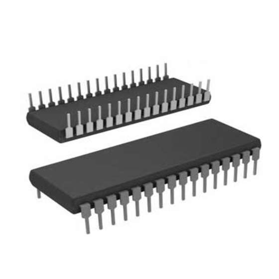
MC80F0704/0708/0804/0808 1.4 Ordering Information Device name FLASH ROM Package MC80F0704G 28SKDIP MC80F0704D 28SOP MC80F0704U 4K bytes 256 bytes 28QFN MC80F0804K 32SDIP MC80F0804D 32SOP MC80F0708G 28SKDIP MC80F0708D 28SOP MC80F0708U 8K bytes 256 bytes 28QFN MC80F0808K 32SDIP MC80F0808D 32SOP Pb free package: For example;... -
Page 10: Block Diagram
MC80F0704/0708/0804/0808 2. BLOCK DIAGRAM Accumulator Stack Pointer Data Memory Program RESET System controller Memory System 8-bit Basic Data Table Clock Controller Interval Interrupt Controller Timer Timing generator Clock Generator Instruction Decoder 10-bit 8-bit High Buzzer Timer/ Speed Watch-dog Driver Converter... -
Page 11: Pin Assignment
MC80F0704/0708/0804/0808 3. PIN ASSIGNMENT 32SDIP/SOP 28 SKDIP/ SOP R04/AN4 / EC0 R03 / AN3 / INT2 R04 / AN4 / EC0 R03 / AN3 / INT2 R05 / AN5 / T0O R02 / AN2 / SOUT R05 / AN5 / T0O... -
Page 12: Package Drawing
MC80F0704/0708/0804/0808 4. PACKAGE DRAWING 28 SKINNY DIP unit: inch 0.314 1.389 0.306 0.292 1.381 0.284 0.349 0.022 0.341 0.067 0.014 TYP 0.100 0.059 October 31, 2011 Ver 1.03... - Page 13 MC80F0704/0708/0804/0808 28 SOP unit: millimetres 5 ~ 15° 17.90 GAUGE PLANE SEATING PLANE 0.51 1.27 0 ~ 8° 0.31 1.27 BSC 5 ~ 15° 0.40 1.40 REF 1. 17.90 dimension does not include mold FLASH, protrusions or gate burrs. Mold FLASH, protrusions or gate burrs shall not exceed 0.15mm per end.
- Page 14 MC80F0704/0708/0804/0808 32 SDIP unit: millimeter TYP 10.16 29.60 9.30 29.20 8.90 0.55 0 ~ 15° 1.10 0.35 TYP 1.778 0.90 32 SOP unit: millimeter 21.30 21.20 0.45 0 ~ 8° 0.95 0.35 TYP 1.27 0.55 October 31, 2011 Ver 1.03...
- Page 15 MC80F0704/0708/0804/0808 28 QFN unit: millimetres Top View Bottom View 0.550 5.10 0.450 4.90 3.250 3.050 0.300 0.180 MIN. NORM. MAX. 0.700 0.750 0.800 0.800 0.850 0.900 Side View October 31, 2011 Ver 1.03...
-
Page 16: Pin Function
MC80F0704/0708/0804/0808 5. PIN FUNCTION : Supply voltage. in Table 5-2 : Circuit ground. Port pin Alternate function RESET: Reset the MCU. AN0 ( Analog Input Port 0 ) : Input to the inverting oscillator amplifier and input to the in- AVref ( External Analog Reference Pin ) ternal main clock operating circuit. - Page 17 MC80F0704/0708/0804/0808 Pin No. Function PIN NAME In/Out First Second Third Forth Supply voltage Circuit ground Input only port RESET (R35) Reset signal input Normal I/O Port (R33) Oscillation Input Normal I/O Port (R34) Oscillation Output R00 (INT3/SCK) External Interrupt 3...
-
Page 18: Port Structures
MC80F0704/0708/0804/0808 6. PORT STRUCTURES R13~R16,R20~R22,R27 R01 (AN1 / SI) Pull-up Pull-up Pull-up Reg. Pull-up Reg. Open Drain Reg. Open Drain Reg. Data Reg. Data Reg. Direction Reg. Direction Reg. Data Bus Data Bus AN[1] ADEN & ADS[3:0] (ADCM) Noise Filter... - Page 19 MC80F0704/0708/0804/0808 R11 (INT0 / PWM3O), R12 (INT1 / BUZO) R00 (INT3 / SCK) Pull-up Pull-up Pull-up Pull-up Reg. Reg. Open Drain Open Drain Reg. Reg. Data Reg. Data Reg. PWM3O, BUZO SCKO_EN(SIOM) PWM3OE(PSR0.7) BUZOE(PSR1.2) Direction Direction Reg. Reg. Data Bus...
- Page 20 MC80F0704/0708/0804/0808 R10 (AN0 / AV / PWM1O) RESET Pull-up Pull-up Reg. Open Drain Reg. Data Reg. Pull-up Pull-up PWM1O Reg. PWM1OE(PSR0.6) Mask only Direction Reg. Data Bus Data Bus Internal Reset Reset Disable (Configuration option bit) AN[0] ADEN & ADS[3:0]...
- Page 21 MC80F0704/0708/0804/0808 (External RC or R oscillation) R33 (X ), R34 (X Pull-up Pull-up Reg. Open Drain Reg. Data Reg. Direction Reg. / R33 STOP MAIN Data Bus CLOCK IN4MCLK IN2MCLK ÷ 4 IN4MCLKXO IN2MCLKXO CLOCK option (Configuration option bit) IN4MCLK...
-
Page 22: Electrical Characteristics
MC80F0704/0708/0804/0808 7. ELECTRICAL CHARACTERISTICS 7.1 Absolute Maximum Ratings Supply voltage............-0.3 to +6.0 V ....................10 mA Storage Temperature ..........-65 to +125 °C Maximum current (ΣI ) ..........160 mA Voltage on any pin with respect to Ground (V Maximum current (ΣI )...........80 mA... -
Page 23: Dc Electrical Characteristics
MC80F0704/0708/0804/0808 1. If the AV voltage is less than V voltage and anlalog input pins(ANX), shared with various alternate function, are used bidirectional I/O port, the leakage current may flow V pin to AV pin in output high mode or anlalog input pins(ANX) to AV pin in input high mode. -
Page 24: Ac Characteristics
MC80F0704/0708/0804/0808 Specifications Parameter Symbol Condition Unit Min. Typ. Max. =5.5V ÷ RC-OSC External RC XOUT RC-OSC R=30kΩ, C=10pF Oscillator Frequency ÷ =5.5V, R=30kΩ R-OSC XOUT R-OSC 1. Hysteresis Input: INT0 ~INT3(R11,R12,R03,R00),SIO(R00,R01,R02), EC0,EC1(R04,R07) 2. This parameter is measured in internal PROM operation at the all I/O port defined input mode. - Page 25 MC80F0704/0708/0804/0808 -0.5V 0.5V RESET 0.2V 0.8V INT0, INT1 0.2V INT3 INT2, EC0, Figure 7-2 Timing Chart October 31, 2011 Ver 1.03...
-
Page 26: Typical Characteristics
MC80F0704/0708/0804/0808 7.6 Typical Characteristics These graphs and tables provided in this section are for design specified range. guidance only and are not tested or guaranteed. The data presented in this section is a statistical summary of data In some graphs or tables the data presented are out- collected on units from different lots over a period of time. - Page 27 MC80F0704/0708/0804/0808 −V −V (mA) (mA) -25°C -25°C 25°C 25°C 85°C 85°C −V −V −V Hysteresis input Normal input , RESET =4kHz =4kHz =4MHz Ta=25°C Ta=25°C Ta=25°C −V −V −V Hysteresis input Normal input , RESET =4kHz =4kHz =4MHz Ta=25°C Ta=25°C Ta=25°C...
- Page 28 MC80F0704/0708/0804/0808 Typical RC Oscillator Typical RC Oscillator Frequency vs V Frequency vs V (MHz) (MHz) = 10pF No Cap Ta = 25°C Ta = 25°C R = 4.7K R = 4.7K R = 10K R = 10K R = 20K...
- Page 29 MC80F0704/0708/0804/0808 by sample, voltage and temperature. The internal oscilla- tion can be used only in timing insensitive application. Typical Internal 4MHz Frequency vs V (MHz) Ta = 25°C Note: The internal 4MHz oscillation frequencies shown in above are provided for design guidance only and not tested or guaranteed.
-
Page 30: Memory Organization
MC80F0704/0708/0804/0808 8. MEMORY ORGANIZATION The MC80F0704/0708/0804/0808 has separate address spaces Data memory can be read and written to up to 256 bytes including for Program memory and Data Memory. 4K bytes program mem- the stack area. ory can only be read, not written to. - Page 31 MC80F0704/0708/0804/0808 V G B H RESET VALUE: 00 CARRY FLAG RECEIVES NEGATIVE FLAG CARRY OUT OVERFLOW FLAG ZERO FLAG SELECT DIRECT PAGE INTERRUPT ENABLE FLAG when G=1, page is selected to “page 1” BRK FLAG HALF CARRY FLAG RECEIVES CARRY OUT FROM BIT 1 OF...
- Page 32 MC80F0704/0708/0804/0808 At execution of At acceptance At execution At execution a CALL/TCALL/PCALL of interrupt of RET instruction of RET instruction Push 01FF 01FF 01FF 01FF down Push 01FE 01FE 01FE 01FE down 01FD 01FD 01FD 01FD 01FC 01FC 01FC 01FC...
-
Page 33: Program Memory
MC80F0704/0708/0804/0808 8.2 Program Memory A 16-bit program counter is capable of addressing up to 64K Example: Usage of TCALL bytes, but this device has 4K/8K/16K bytes program memory space only physically implemented. Accessing a location above FFFF will cause a wrap-around to 0000 ;1BYTE INSTRUCTION... - Page 34 MC80F0704/0708/0804/0808 Address Program Memory PCALL Area Memory Address 0FFC0 0FF00 TCALL 15 TCALL 14 TCALL 13 TCALL 12 TCALL 11 TCALL 10 TCALL 9 TCALL 8 PCALL Area (256 Bytes) TCALL 7 TCALL 6 TCALL 5 TCALL 4 TCALL 3...
-
Page 35: Data Memory
User Memory When returning from the processing routine, executing the sub- The MC80F0704/0708/0804/0808 has 256 × 8 bits for the user routine return instruction [RET] restores the contents of the pro- memory (RAM). RAM pages are selected by RPR (See Figure 8- gram counter from the stack;... - Page 36 MC80F0704/0708/0804/0808 Initial Value Addressing Address Register Name Symbol Mode 7 6 5 4 3 2 1 0 00C0 R0 port data register 0 0 0 0 0 0 0 0 byte, bit 00C1 R0 port I/O direction register R0IO 0 0 0 0 0 0 0 0...
- Page 37 MC80F0704/0708/0804/0808 Initial Value Addressing Address Register Name Symbol Mode 7 6 5 4 3 2 1 0 00DB Timer 3 PWM high register T3PWHR - - - - 0 0 0 0 byte 00E0 Buzzer driver register BUZR 1 1 1 1 1 1 1 1...
- Page 38 MC80F0704/0708/0804/0808 Bit 7 Address Name Bit 6 Bit 5 Bit 4 Bit 3 Bit 2 Bit 1 Bit 0 0C0H R0 Port Data Register 0C1H R0IO R0 Port Direction Register 0C2H R1 Port Data Register 0C3H R1IO R1 Port Direction Register...
- Page 39 MC80F0704/0708/0804/0808 Bit 7 Address Name Bit 6 Bit 5 Bit 4 Bit 3 Bit 2 Bit 1 Bit 0 0EEH IEDS IED3H IED3L IED2H IED2L IED1H IED1L IED0H IED0L 0EFH ADCM ADEN ADCK ADS3 ADS2 ADS1 ADS0 ADST ADSF 0F0H...
-
Page 40: Addressing Mode
MC80F0704/0708/0804/0808 8.4 Addressing Mode Direct Page Addressing → dp The MC8 series MCU uses six addressing modes; • Register addressing In this mode, a address is specified within direct page. • Immediate addressing Example; G=0 ;A ←RAM[35H] • Direct page addressing C535 •... -
Page 41: Indexed Addressing
MC80F0704/0708/0804/0808 ;A ←ROM[135H] 983501 !0135H À data 135H data data → Ã þ → À data+1 → data 0F100H þ 0F101H address: 0135 0F102H X indexed direct page (8 bit offset) → dp+X This address value is the second byte (Operand) of command plus Indexed Addressing the data of X-register. -
Page 42: Indirect Addressing
MC80F0704/0708/0804/0808 D500FA !0FA00H+Y 1625 [25H+X] 0F100H þ 0F101H À 0E005H 0F102H 0FA00H+55H=0FA55H þ 25 + X(10) = 35H 0E005H data À 0FA55H data data → Ã 0FA00H Ã A + data + C → Indirect Addressing Y indexed indirect → [dp]+Y Direct page indirect →... - Page 43 MC80F0704/0708/0804/0808 1F25E0 [!0C025H] PROGRAM MEMORY 0E025H 0E026H À jump to address 0E30AH þ 0E725H NEXT 0FA00H October 31, 2011 Ver 1.03...
-
Page 44: I/O Ports
MC80F0704/0708/0804/0808 9. I/O PORTS The MC80F0704/0708/0804/0808 has three ports (R0, R1 and R3). These ports pins may be multiplexed with an alternate func- tion for the peripheral features on the device. All port can drive WRITE “55 ” TO PORT R0 DIRECTION REGISTER maximum 20mA of high current in output low state, so it can di- rectly drive LED device. -
Page 45: Alternate Function
MC80F0704/0708/0804/0808 tion is selected by writing “1” in the corresponding bit of PSR0 or PSR1, port pin can be used as a corresponding alternate fea- Port Pin Alternate Function tures regardless of the direction register R0IO. R00- INT3 (External interrupt 3) - Page 46 MC80F0704/0708/0804/0808 ADDRESS: 0F8 RESET VALUE: 0000 0000 ADDRESS: 0C2 R1 Data Register RESET VALUE: 00 PSR0 PWM3OE PWM1OE EC1E EC0E INT3E INT2E INT1E INT0E R17 R16 R15 R14 R13 R12 R11 R10 Port / INT Selection Input / Output data...
-
Page 47: R2 And R2Io Register
MC80F0704/0708/0804/0808 9.3 R2 and R2IO register R2 is an 8-bit CMOS bidirectional I/O port (address 0C4 ). Each I/O pin can independently used as an input or an output through the R3IO register (address 0C5 ). When R20 through R27 pins... -
Page 48: R3 And R3Io Register
MC80F0704/0708/0804/0808 9.4 R3 and R3IO register R3 is a 6-bit CMOS bidirectional I/O port (address 0C6 ). Each I/O pin (except R35) can independently used as an input or an output through the R3IO register (address 0C7 ). R35 is an input... -
Page 49: Clock Generator
MC80F0704/0708/0804/0808 10. CLOCK GENERATOR As shown in Figure 10-1 , the clock generator produces the basic through a divide-by-two flip-flop, but minimum and maximum clock pulses which provide the system clock to be supplied to the high and low times specified on the data sheet must be observed. - Page 50 Figure 10-4 External Clock Connections To use the internal 4MHz/2MHz oscillation, the CLK option of In addition, the MC80F0704/0708/0804/0808 has an ability for the configuration bits should be set to “IN4MCLK”, the external RC oscillated operation. It offers additional cost sav- “IN2MCLK”, “IN4MCLKXO”...
-
Page 51: Basic Interval Timer
MC80F0704/0708/0804/0808 11. BASIC INTERVAL TIMER The MC80F0704/0708/0804/0808 has one 8-bit Basic Interval If the STOP instruction executed after writing "1" to bit RCWDT Timer that is free-run and can not stop. Block diagram is shown of CKCTLR, it goes into the internal RC oscillated watchdog tim- in Figure 11-1 . -
Page 52: Source Clock
MC80F0704/0708/0804/0808 Interrupt (overflow) Period (ms) CKCTLR Source clock = 8MHz [2:0] ÷8 0.256 ÷16 0.512 ÷32 1.024 ÷64 2.048 ÷128 4.096 ÷256 8.192 16.384 ÷512 32.768 ÷1024 Table 11-1 Basic Interval Timer Interrupt Period ADDRESS: 0F2 CKCTLR BTCL BTS2 BTS1... -
Page 53: Watchdog Timer
MC80F0704/0708/0804/0808 12. WATCHDOG TIMER The watchdog timer rapidly detects the CPU malfunction such as RCWDT as shown below. endless looping caused by noise or the like, and resumes the CPU CKCTLR,#3FH; enable the RC-OSC WDT to the normal state. The watchdog timer signal for detecting mal- WDTR,#0FFH ;... - Page 54 MC80F0704/0708/0804/0808 time, selecting of output, and clearing of the binary counter. low to reset the internal hardware. When WDTON=0, a watchdog Clearing the binary counter is repeated within the detection time. timer interrupt (WDTIF) is generated. The WDTON bit is in reg- ister CLKCTLR.
- Page 55 MC80F0704/0708/0804/0808 Source clock BIT overflow Binary-counter Counter Counter Clear Clear WDTR Match Detect WDTIF interrupt WDTR ← “1000_0011 ” WDT reset reset Figure 12-3 Watchdog timer Timing If the watchdog timer output becomes active, a reset is generated, set is generated in sub clock mode.
-
Page 56: Timer/Event Counter
MC80F0704/0708/0804/0808 13. TIMER/EVENT COUNTER The MC80F0704/0708/0804/0808 has Four Timer/Counter reg- counter function. When external clock edge input, the count reg- isters. Each module can generate an interrupt to indicate that an ister is captured into Timer data register correspondingly. When event has occurred (i.e. - Page 57 MC80F0704/0708/0804/0808 ADDRESS: 0D0 CAP0 T0CK2 T0CK1 BTCL T0CK0 T0CN T0ST INITIAL VALUE: --00 0000 Bit Name Bit Position Description CAP0 TM0.5 0: Timer/Counter mode 1: Capture mode selection flag T0CK2 TM0.4 000: 8-bit Timer, Clock source is f ÷ T0CK1 TM0.3...
- Page 58 MC80F0704/0708/0804/0808 ADDRESS: 0D6 CAP2 T2CK2 T2CK1 BTCL T2CK0 T2CN T2ST INITIAL VALUE: --00 0000 Bit Name Bit Position Description CAP2 TM2.5 0: Timer/Counter mode 1: Capture mode selection flag T2CK2 TM2.4 000: 8-bit Timer, Clock source is f ÷ T2CK1 TM2.3...
-
Page 59: 8-Bit Timer / Counter Mode
MC80F0704/0708/0804/0808 13.1 8-bit Timer / Counter Mode The MC80F0704/0708/0804/0808 has four 8-bit Timer/ PWM3E of TM1 or TM3 should be cleared to "0" (Figure 13-3 ). Counters, Timer 0, Timer 1, Timer 2, Timer 3. The Timer 0, Tim- These timers have each 8-bit count register and data register. The... - Page 60 MC80F0704/0708/0804/0808 ADDRESS: 0D6 CAP2 T2CK2 T2CK1 BTCL T2CK0 T2CN T2ST INITIAL VALUE: --000000 X means don’t care ADDRESS: 0D8 16BIT CAP3 T3CK1 BTCL T3CK0 T3CN T3ST PWM3E INITIAL VALUE: 00 X means don’t care T2CK[2:0] EDGE DETECTOR EC1 PIN T2ST ÷...
- Page 61 MC80F0704/0708/0804/0808 Example 1: These timers have each 8-bit count register and data register. The count register is increased by every internal or external clock in- Timer0 = 2ms 8-bit timer mode at 4MHz put. The internal clock has a prescaler divide ratio option of 2, 4, Timer1 = 0.5ms 8-bit timer mode at 4MHz...
- Page 62 MC80F0704/0708/0804/0808 Example: Make 1ms interrupt using by Timer0 at 4MHz TM0,#0FH ; divide by 32 TDR0,#124 ; 8us x (124+1)= 1ms SET1 ; Enable Timer 0 Interrupt ; Enable Master Interrupt When TM0 = 0000 1111 (8-bit Timer mode, Prescaler divide ratio = 32)
- Page 63 MC80F0704/0708/0804/0808 TDR1 enable disable clear & start stop TIME Timer 1 (T1IF) Interrupt Occur interrupt Occur interrupt T1ST T1ST = 1 Start & Stop T1ST = 0 T1CN T1CN = 1 Control count T1CN = 0 Figure 13-8 Count Operation of Timer / Event counter...
-
Page 64: 16-Bit Timer / Counter Mode
MC80F0704/0708/0804/0808 13.2 16-bit Timer / Counter Mode The Timer register is being run with all 16 bits. A 16-bit timer/ The clock source of the Timer 2 is selected either internal or ex- counter register T0, T1 are incremented from 0000 until it ternal clock by bit T2CK[2:0]. -
Page 65: 8-Bit Compare Output (16-Bit)
Figure 13-10 16-bit Timer/Counter for Timer 2, 3 13.3 8-bit Compare Output (16-bit) The MC80F0704/0708/0804/0808 has Timer Compare Output nal having a 50 : 50 duty square wave, and output frequency is function. To pulse out, the timer match can goes to port pin (T0O same as below equation. - Page 66 MC80F0704/0708/0804/0808 of Timer. ter captured, Timer x register is cleared and restarts by hardware. It has three transition modes: "falling edge", "rising edge", "both For example, in Figure 13-14 , the pulse width of captured signal edge" which are selected by interrupt edge selection register is wider than the timer data value (FF ) over 2 times.
- Page 67 MC80F0704/0708/0804/0808 ADDRESS: 0D0 CAP0 T0CK2 BTCL T0CK1 T0CK0 T0CN T0ST INITIAL VALUE: --00 0000 X means don’t care ADDRESS: 0D2 16BIT CAP1 BTCL T1CK1 T1CK0 T1CN T1ST PWM1E INITIAL VALUE: 00 X means don’t care T0CK[2:0] Edge Detector EC0 PIN T0ST ÷...
- Page 68 MC80F0704/0708/0804/0808 ADDRESS: 0D6 CAP2 T2CK2 BTCL T2CK1 T2CK0 T2CN T2ST INITIAL VALUE: --00 0000 X means don’t care ADDRESS: 0D8 16BIT CAP3 BTCL T3CK1 T3CK0 T3CN T3ST PWM3E INITIAL VALUE: 00 X means don’t care T2CK[2:0] Edge Detector EC1 PIN T2ST ÷...
- Page 69 MC80F0704/0708/0804/0808 This value is loaded to CDR0 TIME Ext. INT0 Pin Interrupt Request ( INT0IF ) Interrupt Interval Period Ext. INT0 Pin Interrupt Request ( INT0IF ) 20nS Delay Clear & Start Capture ( Timer Stop ) Figure 13-13 Input Capture Operation of Timer 0 Capture mode Ext.
-
Page 70: 16-Bit Capture Mode
MC80F0704/0708/0804/0808 13.5 16-bit Capture Mode 16-bit capture mode is the same as 8-bit capture, except that the The clock source of the Timer 2 is selected either internal or ex- Timer register is being run will 16 bits. The clock source of the ternal clock by bit T2CK[2:0]. - Page 71 MC80F0704/0708/0804/0808 ADDRESS: 0D6 CAP2 T2CK2 T2CK1 BTCL T2CK0 T2CN T2ST INITIAL VALUE: --00 0000 X means don’t care ADDRESS: 0D8 16BIT CAP3 T3CK1 BTCL T3CK0 T3CN T3ST PWM3E INITIAL VALUE: 00 X means don’t care T2CK[2:0] Edge Detector EC1 PIN T2ST ÷...
-
Page 72: Pwm Mode
MC80F0704/0708/0804/0808 13.6 PWM Mode The MC80F0704/0708/0804/0808 has high speed PWM (Pulse resolution. Width Modulation) functions which shared with Timer1 or Timer3. Frequency In PWM mode, R10 / PWM1O or R11 / PWM3O pin output up Resolution T1CK[1:0] T1CK[1:0] T1CK[1:0] to a 10-bit resolution PWM output. These pins should be config-... -
Page 73: Initial Value
MC80F0704/0708/0804/0808 ADDRESS: 0D2 16BIT CAP3 T3CK1 BTCL T3CK0 T3CN T3ST PWM1E INITIAL VALUE: 00 X:The value "0" or "1" corresponding your operation. ADDRESS: 0D5 T1PWHR BTCL T3PWHR3 T3PWHR2 T3PWHR1 T3PWHR0 INITIAL VALUE: ---- 0000 Bit Manipulation Not Available X:The value "0" or "1" corresponding your operation. - Page 74 MC80F0704/0708/0804/0808 ADDRESS: 0D8 16BIT CAP3 T3CK1 BTCL T3CK0 T3CN T3ST PWM3E INITIAL VALUE: 00 X:The value "0" or "1" corresponding your operation. ADDRESS: 0DB T3PWHR BTCL T3PWHR3 T3PWHR2 T3PWHR1 T3PWHR0 INITIAL VALUE: ---- 0000 Bit Manipulation Not Available X:The value "0" or "1" corresponding your operation.
- Page 75 MC80F0704/0708/0804/0808 Source clock PWM1E T1ST T1CN PWM1O [POL=1] PWM1O [POL=0] Duty Cycle [ (1+7Fh) x 250nS = 32uS ] Period Cycle [ (3FFh+1) x 250nS = 256uS, 3.9KHz ] T1CK[1:0] = 00 ( XIN ) T1PPR (8-bit) Period T1PWHR3 T1PWHR2...
-
Page 76: Analog To Digital Converter
MC80F0704/0708/0804/0808 14. ANALOG TO DIGITAL CONVERTER The analog-to-digital converter (A/D) allows conversion of an set to “1”. After one cycle, it is cleared by hardware. The register analog input signal to a corresponding 10-bit digital value. The A/ ADCRH and ADCRL contains the results of the A/D conversion. - Page 77 MC80F0704/0708/0804/0808 may not be obtainable due to coupling noise. Therefore, avoid ap- ply voltage error plying pulses to pins adjacent to the pin undergoing A/D conver- sion. Note: If the AV voltage is less than V voltage and an- lalog input pins(ANX), shared with various alternate func-...
- Page 78 MC80F0704/0708/0804/0808 ADDRESS: 0EF ADCM BTCL ADEN ADCK ADS3 ADS2 ADS1 ADS0 ADST ADSF INITIAL VALUE: 0000 0001 A/D status bit 0: A/D conversion is in progress 1: A/D conversion is completed A/D start bit Setting this bit starts an A/D conversion.
-
Page 79: Serial Input/Output (Sio)
MC80F0704/0708/0804/0808 15. SERIAL INPUT/OUTPUT (SIO) The serial Input/Output is used to transmit/receive 8-bit data se- control circuit as illustrated in Figure 15-1 . The SO pin is de- rially. The Serial Input/Output (SIO) module is a serial interface signed to input and output. So the Serial I/O(SIO) can be operated useful for communicating with other peripheral of microcontrol- with minimum two pin. -
Page 80: Transmission/Receiving Timing
MC80F0704/0708/0804/0808 Serial I/O Mode Register (SIOM) controls serial I/O function. Serial I/O Data Register (SIOR) is an 8-bit shift register. First According to SCK1 and SCK0, the internal clock or external LSB is send or is received first. clock can be selected. - Page 81 MC80F0704/0708/0804/0808 SIOST SCK [R00] (POL=0) SO [R02] SI [R01] (IOSW=0) IOSWIN [R02] (IOSW=1) SIOIF (SIO Int. Req) SIOSF (SIO Status) Figure 15-3 Serial I/O Timing Diagram at POL=0 SIOST SCK [R00] (POL=1) SO [R02] SI [R01] (IOSW=0) IOSWIN [R02] (IOSW=1) SIOIF (SIO Int.
-
Page 82: The Usage Of Serial I/O
MC80F0704/0708/0804/0808 15.2 The usage of Serial I/O 1. Select transmission/receiving mode. SIOR,#0AAh ;set tx data 2. In case of sending mode, write data to be send to SIOR. SIOM,#0011_1100b;set SIO mode 3. Set SIOST to “1” to start serial transmission. -
Page 83: Buzzer Function
MC80F0704/0708/0804/0808 16. BUZZER FUNCTION The buzzer driver block consists of 6-bit binary counter, buzzer driving. register BUZR, and clock source selector. It generates square- Equation of frequency calculation is shown below. wave which has very wide range frequency (488Hz ~ 250kHz at = 4MHz) by user software. - Page 84 MC80F0704/0708/0804/0808 The 6-bit counter is cleared and starts the counting by writing sig- When main-frequency is 4MHz, buzzer frequency is shown as nal at BUZR register. It is incremental from 00 until it matches below Table 16-1. 6-bit BUR value.
-
Page 85: Interrupts
MC80F0704/0708/0804/0808 17. INTERRUPTS The MC80F0704/0708/0804/0808 interrupt circuits consist of In- The Timer 0 ~ Timer 3 Interrupts are generated by T0IF, T1IF, terrupt enable register (IENH, IENL), Interrupt request flags of T2IF and T3IF which is set by a match in their respective timer/ IRQH, IRQL, Priority circuit, and Master enable flag (“I”... - Page 86 MC80F0704/0708/0804/0808 The SIO interrupt is generated by SIOIF which is set by comple- tion of SIO data reception or transmission. Reset/Interrupt Symbol Priority The interrupts are controlled by the interrupt master enable flag I-flag (bit 2 of PSW on Figure 8-3 ), the interrupt enable register...
- Page 87 MC80F0704/0708/0804/0808 ADDRESS: 0EA IENH INT0E INT1E INT2E INT3E SIOE INITIAL VALUE: 0000 --00 Timer/Counter 0 interrupt enable flag Serial Communication interrupt enable flag External interrupt 3 enable flag External interrupt 2 enable flag External interrupt 1 enable flag External interrupt 0 enable flag...
-
Page 88: Interrupt Sequence
MC80F0704/0708/0804/0808 Figure 17-3 Interrupt Request Flag Register 17.1 Interrupt Sequence An interrupt request is held until the interrupt is accepted or the =4MHz) after the completion of the current instruction interrupt latch is cleared to “0” by a reset or an instruction. Inter- execution. -
Page 89: Brk Interrupt
MC80F0704/0708/0804/0808 Example: Clearing Interrupt Request Flag Note: The MC80F0708 and HMS87C1416B is similar in function, but the interrupt processing method is different. T1_INT: CLR1 T1IF ;CLEAR T1 REQUEST When replacing the HMS87C1416B to MC80F0708, clear- ing interrupt request flag should be added. - Page 90 MC80F0704/0708/0804/0808 interrupt can be serviced even if certain interrupt is in progress. Main Program service TIMER 1 service INT0 service enable INT0 disable other In this example, the INT0 interrupt can be serviced without any Occur Occur pending, even TIMER1 is in progress.
-
Page 91: External Interrupt
MC80F0704/0708/0804/0808 17.4 External Interrupt The external interrupt on INT0, INT1, INT2 and INT3 pins are The edge detection of external interrupt has three transition acti- edge triggered depending on the edge selection register IEDS (ad- vated mode: rising edge, falling edge, and both edge. - Page 92 MC80F0704/0708/0804/0808 ADDRESS: 0EE IEDS IED3H IED3L IED2H IED2L IED1H BTCL IED1L IED0H IED0L INITIAL VALUE: 00 INT3 INT2 INT1 INT0 Edge selection register 00: Reserved 01: Falling (1-to-0 transition) 10: Rising (0-to-1 transition) 11: Both (Rising & Falling) ADDRESS: 0F8...
-
Page 93: Power Saving Operation
MC80F0704/0708/0804/0808 18. POWER SAVING OPERATION The MC80F0704/0708/0804/0808 has two power-down modes. tions, STOP mode and SLEEP mode. Table 18-1 shows the status In power-down mode, power consumption is reduced of each Power Saving Mode. SLEEP mode is entered by the considerably. -
Page 94: Stop Mode
MC80F0704/0708/0804/0808 Oscillator pin) Internal Clock External Interrupt SLEEP Instruction Executed Normal Operation SLEEP Operation Normal Operation Figure 18-2 SLEEP Mode Release Timing by External Interrupt Oscillator pin) Clock RESET Internal RESET SLEEP Instruction Stabilization Time Execution = 65.5mS @4MHz Normal Operation... - Page 95 MC80F0704/0708/0804/0808 the power dissipation associated with the pin interface (depend- Note: After STOP instruction, at least two or more NOP instruc- ing on the external circuitry and program) is not directly deter- tion should be written. mined by the hardware operation of the STOP feature. This point LDM CKCTLR,#0FH ;more than 20ms...
- Page 96 MC80F0704/0708/0804/0808 STOP INSTRUCTION STOP Mode Interrupt Request Corresponding Interrupt IENH or IENL ? Enable Bit (IENH, IENL) STOP Mode Release Master Interrupt I-FLAG Enable Bit PSW[2] Interrupt Service Routine Next INSTRUCTION Figure 18-4 STOP Releasing Flow by Interrupts Oscillator pin)
-
Page 97: Stop Mode At Internal Rc-Oscillated Watchdog Timer Mode
MC80F0704/0708/0804/0808 STOP Mode Oscillator (XI pin) Internal Clock RESET Internal RESET STOP Instruction Execution Stabilization Time Time can not be control by software = 65.5mS @4MHz Figure 18-6 Timing of STOP Mode Release by Reset 18.3 Stop Mode at Internal RC-Oscillated Watchdog Timer Mode In the Internal RC-Oscillated Watchdog Timer mode, the on-chip (at RC-watchdog timer mode). - Page 98 MC80F0704/0708/0804/0808 Oscillator pin) Internal RC Clock Internal Clock External Interrupt ( or WDT Interrupt ) Clear Basic Interval Timer STOP Instruction Execution Counter Normal Operation Stabilization Time STOP mode Normal Operation at RC-WDT Mode > 20mS Figure 18-7 Stop Mode Release at Internal RC-WDT Mode by External Interrupt or WDT Interrupt...
-
Page 99: Minimizing Current Consumption
MC80F0704/0708/0804/0808 18.4 Minimizing Current Consumption The Stop mode is designed to reduce power consumption. To off output drivers that are sourcing or sinking current, if it is prac- minimize current drawn during Stop mode, the user should turn- tical. INPUT PIN... - Page 100 MC80F0704/0708/0804/0808 ) is applied to input pin, there can be little current (max. 1mA nal circuit. For example, if there is external pull-up resistor then at around 2V) flow. it is set to output mode, i.e. to High, and if there is external pull- down register, it is set to low.
-
Page 101: Reset
MC80F0704/0708/0804/0808 19. RESET The MC80F0704/0708/0804/0808 supports various kinds of reset • Watchdog Timer Timeout Reset as below. • Power-Fail Detection (PFD) Reset • Power-On Reset (POR) • Address Fail Reset • RESET (external reset circuitry) RESET Noise Canceller (Power-On Reset) -
Page 102: Main Program
MC80F0704/0708/0804/0808 Oscillator pin) RESET ADDRESS FFFE FFFF Start DATA MAIN PROGRAM Reset Process Step Stabilization Time =65.5mS at 4MHz x 256 ÷1024 Figure 19-3 Timing Diagram after Reset The Address Fail Reset is the function to reset the system by code area or RAM area, the address fail reset is occurred. -
Page 103: Power Fail Processor
MC80F0704/0708/0804/0808 20. POWER FAIL PROCESSOR The MC80F0704/0708/0804/0808 has an on-chip power fail de- Fail Voltage Detector Register” on page 97. tection circuitry to immunize against power noise. A configura- In the in-circuit emulator, power fail function is not implemented tion register, PFDR, can enable or disable the power fail detect and user can not experiment with it. - Page 104 MC80F0704/0708/0804/0808 65.5mS Internal RESET When PFDM = 1 65.5mS Internal t < 65.5mS RESET 65.5mS Internal RESET Figure 20-3 Power Fail Processor Situations (at 4MHz operation) October 31, 2011 Ver 1.03...
-
Page 105: Countermeasure Of Noise
“ONP” bit of the Device - Change system clock to the internal oscillation clock configuration area (20FF ) for the MC80F0704/0708/0804/ when the X is shorted or opened, the main 0808, “ONP” option bits MASK option. -
Page 106: Oscillation Fail Processor
21.2 Oscillation Fail Processor The oscillation fail processor (OFP) can change the clock source Configuration Area (MASK option for MC80F0704/0708/0804/ from external to internal oscillator when the oscillation fail oc- 0808 enables the function to operate the device by using the in- curred. -
Page 107: Device Configuration Area
MC80F0704/0708/0804/0808 Device Configuration Area The Device Configuration Area can be programmed or left un- Note: The Configuration Option may not be read exactly programmed to select device configuration such as POR, ONP, when VDD rising time is very slow. It is recommended to CLK option and security bit. -
Page 108: Emulator Eva. Board Setting
MC80F0704/0708/0804/0808 23. Emulator EVA. Board Setting À Œ œ – Ã Õ þ October 31, 2011 Ver 1.03... - Page 109 MC80F0704/0708/0804/0808 DIP Switch and VR Setting configuration Before execute the user program, keep in your mind the below DIP S/W Description ON/OFF Setting þ This connector is only used for a device over 32 PIN. For the MC80F0224/MC80F0448 À This connector is only used for a device under 32 PIN.
- Page 110 MC80F0704/0708/0804/0808 DIP S/W Description ON/OFF Setting This switch select the Normal I/O port These switches select the R33 or X œ (on&off) or special function select(off&on). It is reserved for the MC80F0708/0808. These switches select the R34 or X ON & OFF : R33,R34,R35 Port selected.
- Page 111 APPENDIX...
-
Page 112: Instruction
MC80F0704/0708/0804/0808 A. INSTRUCTION A.1 Terminology List Terminology Description Accumulator X - register Y - register Program Status Word #imm 8-bit Immediate data Direct Page Offset Address !abs Absolute Address Indirect expression Register Indirect expression { }+ Register Indirect expression, after that, Register auto-increment .bit... -
Page 113: Instruction Map
MC80F0704/0708/0804/0808 A.2 Instruction Map 00000 00001 00010 00011 00100 00101 00110 00111 01000 01001 01010 01011 01100 01101 01110 01111 HIGH SET1 TCALL SETA1 PUSH dp.bit A.bit,rel dp.bit,rel #imm dp+X !abs .bit TCALL CLRA1 PUSH CLRC “ “ “ #imm... -
Page 114: Instruction Set
MC80F0704/0708/0804/0808 A.3 Instruction Set Arithmetic / Logic Operation BYTE CYCLE FLAG MNEMONIC OPERATION NVGBHIZC CODE ADC #imm ADC dp ADC dp + X ADC !abs Add with carry. NV--H-ZC A ← ( A ) + ( M ) + C... - Page 115 MC80F0704/0708/0804/0808 BYTE CYCLE FLAG MNEMONIC OPERATION CODE NVGBHIZC EOR #imm EOR dp EOR dp + X EOR !abs Exclusive OR N-----Z- EOR !abs + Y A ← ( A ) ⊕ ( M ) EOR [ dp + X ]...
- Page 116 MC80F0704/0708/0804/0808 Register / Memory Operation BYTE CYCLE FLAG MNEMONIC OPERATION CODE NVGBHIZC LDA #imm LDA dp LDA dp + X LDA !abs Load accumulator LDA !abs + Y A ← ( M ) N-----Z- LDA [ dp + X ]...
- Page 117 MC80F0704/0708/0804/0808 16-BIT Operation BYTE CYCLE FLAG MNEMONIC OPERATION NVGBHIZC CODE 16-Bits add without carry ADDW dp NV--H-ZC YA ← ( YA ) + ( dp +1 ) ( dp ) (YA) − Compare YA contents with memory pair contents :...
- Page 118 MC80F0704/0708/0804/0808 Branch / Jump Operation BYTE CYCLE FLAG MNEMONIC OPERATION CODE NVGBHIZC BBC A.bit,rel Branch if bit clear : -------- if ( bit ) = 0 , then pc ← ( pc ) + rel BBC dp.bit,rel BBS A.bit,rel Branch if bit set : -------- if ( bit ) = 1 , then pc ←...
- Page 119 MC80F0704/0708/0804/0808 Control Operation & Etc. BYTE CYCLE FLAG MNEMONIC OPERATION CODE NVGBHIZC Software interrupt : B ← ”1”, M(sp) ← (pc ), sp ←sp-1, M(s) ← (pc ), sp ← sp - 1, M(sp) ← (PSW), sp ← sp -1, ---1-0-- ←...
- Page 120 MC80F0704/0708/0804/0808 October 31, 2011 Ver 1.03...
Need help?
Do you have a question about the MC80F0704 and is the answer not in the manual?
Questions and answers