Sign In
Upload
Download
Table of Contents
Contents
Add to my manuals
Delete from my manuals
Share
URL of this page:
HTML Link:
Bookmark this page
Add
Manual will be automatically added to "My Manuals"
Print this page
×
Bookmark added
×
Added to my manuals
Manuals
Brands
Abov Manuals
Microcontrollers
MC96F6432 Series
User manual
Abov MC96F6432 Series User Manual
8-bit microcontrollers
Hide thumbs
1
2
3
4
Table Of Contents
5
6
7
8
9
10
11
12
13
14
15
16
17
18
19
20
21
22
23
24
25
26
27
28
29
30
31
32
33
34
35
36
37
38
39
40
41
42
43
44
45
46
47
48
49
50
51
52
53
54
55
56
57
58
59
60
61
62
63
64
65
66
67
68
69
70
71
72
73
74
75
76
77
78
79
80
81
82
83
84
85
86
87
88
89
90
91
92
93
94
95
96
97
98
99
100
101
102
103
104
105
106
107
108
109
110
111
112
113
114
115
116
117
118
119
120
121
122
123
124
125
126
127
128
129
130
131
132
133
134
135
136
137
138
139
140
141
142
143
144
145
146
147
148
149
150
151
152
153
154
155
156
157
158
159
160
161
162
163
164
165
166
167
168
169
170
171
172
173
174
175
176
177
178
179
180
181
182
183
184
185
186
187
188
189
190
191
192
193
194
195
196
197
198
199
200
201
202
203
204
205
206
207
208
209
210
211
212
213
214
215
216
217
218
219
220
221
222
223
224
225
226
227
228
229
230
231
232
233
234
235
236
237
238
239
240
241
242
243
244
245
246
247
248
249
250
251
252
253
254
255
256
257
258
259
260
261
262
263
264
265
266
267
268
269
270
271
272
273
274
275
276
277
278
279
280
281
282
283
284
285
286
287
288
289
290
291
292
293
294
295
296
297
298
299
300
301
302
303
304
305
306
307
308
309
310
311
312
313
314
315
316
317
318
319
320
321
322
323
324
325
326
327
page
of
327
Go
/
327
Contents
Table of Contents
Bookmarks
Table of Contents
Table of Contents
1 Overview
Description
Features
Ordering Information
Table 1-1 Ordering Information of MC96F6432
Development Tools
Figure 1.1 Debugger(OCD1/OCD2) and Pin Description
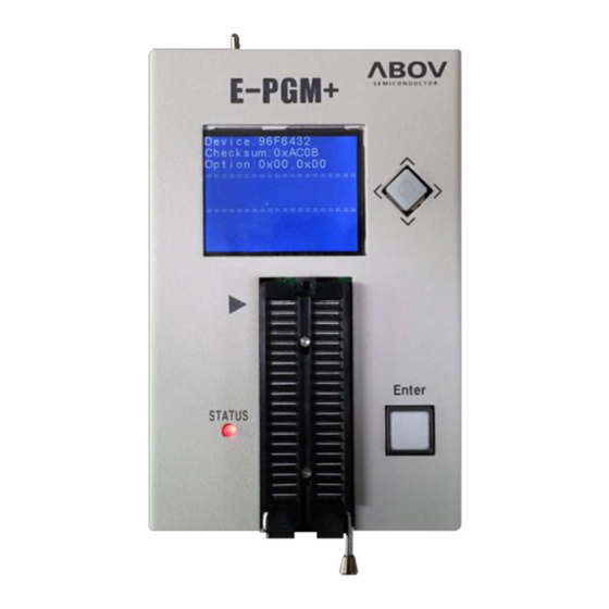
Figure 1.2 E-PGM+(Single Writer)
Figure 1.3 E-GANG4 and E-GANG6 (for Mass Production)
2 Block Diagram
Figure 2.1 Block Diagram
3 Pin Assignment
Figure 3.1 MC96F6432L 48LQFP-0707 Pin Assignment
Figure 3.2 MC96F6432Q 44MQFP-1010 Pin Assignment
Figure 3.3 MC96F6332L 32LQFP Pin Assignment
Figure 3.4 MC96F6332D 32SOP Pin Assignment
Figure 3.5 MC96F6332M 28SOP Pin Assignment
4 Package Diagram
Figure 4.1 48-Pin LQFP-0707 Package
Figure 4.2 44-Pin MQFP Package
Figure 4.3 32-Pin LQFP Package
Figure 4.4 32-Pin SOP Package
Figure 4.5 28-Pin SOP Package
5 Pin Description
Table 5-1 Normal Pin Description
6 Port Structures
General Purpose I/O Port
Figure 6.1 General Purpose I/O Port
External Interrupt I/O Port
Figure 6.2 External Interrupt I/O Port
7 Electrical Characteristics
Absolute Maximum Ratings
Recommended Operating Conditions
Table 7-1 Absolute Maximum Ratings
Table 7-2 Recommended Operating Conditions
A/D Converter Characteristics
Power-On Reset Characteristics
Table 7-3 A/D Converter Characteristics
Table 7-4 Power-On Reset Characteristics
Low Voltage Reset and Low Voltage Indicator Characteristics
Table 7-5 LVR and LVI Characteristics
High Internal RC Oscillator Characteristics
Internal Watch-Dog Timer RC Oscillator Characteristics
Table 7-6 High Internal RC Oscillator Characteristics
Table 7-7 Internal WDTRC Oscillator Characteristics
LCD Voltage Characteristics
Table 7-8 LCD Voltage Characteristics
DC Characteristics
Table 7-9 DC Characteristics
AC Characteristics
Figure 7.1 AC Timing
Table 7-10 AC Characteristics
SPI0/1/2 Characteristics
Figure 7.2 SPI0/1/2 Timing
Table 7-11 SPI0/1/2 Characteristics
UART0/1 Characteristics
Figure 7.3 Waveform for UART0/1 Timing Characteristics
Figure 7.4 Timing Waveform for the UART0/1 Module
Table 7-12 UART0/1 Characteristics
I2C0/1 Characteristics
Figure 7.5 I2C0/1 Timing
Table 7-13 I2C0/1 Characteristics
Data Retention Voltage in Stop Mode
Figure 7.6 Stop Mode Release Timing When Initiated by an Interrupt
Figure 7.7 Stop Mode Release Timing When Initiated by RESETB
Table 7-14 Data Retention Voltage in Stop Mode
Internal Flash Rom Characteristics
Input/Output Capacitance
Table 7-15 Internal Flash Rom Characteristics
Table 7-16 Input/Output Capacitance
Main Clock Oscillator Characteristics
Figure 7.8 Crystal/Ceramic Oscillator
Figure 7.9 External Clock
Table 7-17 Main Clock Oscillator Characteristics
Sub Clock Oscillator Characteristics
Figure 7.10 Crystal Oscillator
Figure 7.11 External Clock
Table 7-18 Sub Clock Oscillator Characteristics
Main Oscillation Stabilization Characteristics
Sub Oscillation Characteristics
Figure 7.12 Clock Timing Measurement at XIN
Figure 7.13 Clock Timing Measurement at SXIN
Table 7-19 Main Oscillation Stabilization Characteristics
Table 7-20 Sub Oscillation Stabilization Characteristics
Operating Voltage Range
Figure 7.14 Operating Voltage Range
Recommended Circuit and Layout
Figure 7.15 Recommended Circuit and Layout
Recommended Circuit and Layout with SMPS Power
Figure 7.16 Recommended Circuit and Layout with SMPS Power
Typical Characteristics
Figure 7.17 RUN (IDD1 ) Current
Figure 7.18 IDLE (IDD2) Current
Figure 7.19 SUB RUN (IDD3) Current
Figure 7.20 SUB IDLE (IDD4) Current
Figure 7.21 STOP (IDD5) Current
8 Memory
Program Memory
Figure 8.1 Program Memory
Data Memory
Figure 8.2 Data Memory Map
Figure 8.3 Lower 128 Bytes RAM
XRAM Memory
Figure 8.4 XDATA Memory Area
SFR Map
Table 8-1 SFR Map Summary
Table 8-2 SFR Map Summary
Table 8-3 SFR Map
9 I/O Ports
Port Register
Table 9-1 Port Register Map
P0 Port
P1 Port
P2 Port
P3 Port
P4 Port
P5 Port
Port Function
10 Interrupt Controller
Overview
Table 10-1 Interrupt Group Priority Level
External Interrupt
Figure 10.1 External Interrupt Description
Block Diagram
Figure 10.2 Block Diagram of Interrupt
Interrupt Vector Table
Interrupt Sequence
Table 10-2 Interrupt Vector Address Table
Figure 10.3 Interrupt Sequence Flow
Effective Timing after Controlling Interrupt Bit
Figure 10.4 Effective Timing of Interrupt Enable Register
Figure 10.5 Effective Timing of Interrupt Flag Register
Multi Interrupt
Figure 10.6 Effective Timing of Multi-Interrupt
Interrupt Enable Accept Timing
Interrupt Service Routine Address
Saving/Restore General-Purpose Registers
Figure 10.7 Interrupt Response Timing Diagram
Figure 10.8 Correspondence between Vector Table Address and the Entry Address of ISR
Figure 10.9 Saving/Restore Process Diagram and Sample Source
Interrupt Timing
Interrupt Register Overview
Figure 10.10 Timing Chart of Interrupt Acceptance and Interrupt Return Instruction
Table 10-3 Interrupt Register Map
11 Peripheral Hardware
Clock Generator
Figure 11.1 Clock Generator Block Diagram
Table 11-1 Clock Generator Register Map
Basic Interval Timer
Figure 11.2 Basic Interval Timer Block Diagram
Table 11-2 Basic Interval Timer Register Map
Watch Dog Timer
Figure 11.3 Watch Dog Timer Interrupt Timing Waveform
Figure 11.4 Watch Dog Timer Block Diagram
Table 11-3 Watch Dog Timer Register Map
Watch Timer
Figure 11.5 Watch Timer Block Diagram
Table 11-4 Watch Timer Register Map
Timer 0
Table 11-5 Timer 0 Operating Modes
Figure 11.6 8-Bit Timer/Counter Mode for Timer 0
Figure 11.7 8-Bit Timer/Counter 0 Example
Figure 11.8 8-Bit PWM Mode for Timer 0
Figure 11.9 PWM Output Waveforms in PWM Mode for Timer 0
Figure 11.10 8-Bit Capture Mode for Timer 0
Figure 11.11 Input Capture Mode Operation for Timer 0
Figure 11.12 Express Timer Overflow in Capture Mode
Figure 11.13 8-Bit Timer 0 Block Diagram
Table 11-6 Timer 0 Register Map
Timer 1
Table 11-7 Timer 1 Operating Modes
Figure 11.14 16-Bit Timer/Counter Mode for Timer 1
Figure 11.15 16-Bit Timer/Counter 1 Example
Figure 11.16 16-Bit Capture Mode for Timer 1
Figure 11.17 Input Capture Mode Operation for Timer 1
Figure 11.18 Express Timer Overflow in Capture Mode
Figure 11.19 16-Bit PPG Mode for Timer 1
Figure 11.20 16-Bit PPG Mode Timming Chart for Timer 1
Figure 11.21 16-Bit Timer 1 Block Diagram
Table 11-8 Timer 2 Register Map
Timer 2
Table 11-9 Timer 2 Operating Modes
Figure 11.22 16-Bit Timer/Counter Mode for Timer 2
Figure 11.23 16-Bit Timer/Counter 2 Example
Figure 11.24 16-Bit Capture Mode for Timer 2
Figure 11.25 Input Capture Mode Operation for Timer 2
Figure 11.26 Express Timer Overflow in Capture Mode
Figure 11.27 16-Bit PPG Mode for Timer 2
Figure 11.28 16-Bit PPG Mode Timming Chart for Timer 2
Figure 11.29 16-Bit Timer 2 Block Diagram
Table 11-10 Timer 3 Register Map
Timer 3, 4
Table 11-11 Timer 3, 4 Operating Modes
Figure 11.30 8-Bit Timer/Counter Mode for Timer 3, 4
Figure 11.31 16-Bit Timer/Counter Mode for Timer 3
Figure 11.32 8-Bit Capture Mode for Timer 3, 4
Figure 11.33 16-Bit Capture Mode for Timer 3
Table 11-12 PWM Frequency Vs. Resolution at 8 Mhz
Table 11-13 PWM Channel Polarity
Figure 11.34 10-Bit PWM Mode (Force 6-Ch)
Figure 11.35 10-Bit PWM Mode (Force All-Ch)
Figure 11.36 Example of PWM at 4 Mhz
Figure 11.37 Example of Changing the Period in Absolute Duty Cycle at 4 Mhz
Figure 11.38 Example of PWM Output Waveform
Figure 11.39 Example of PWM Waveform in Back-To-Back Mode at 4 Mhz
Figure 11.40 Example of Phase Correction and Frequency Correction of PWM
Figure 11.41 Example of PWM External Synchronization with BLNK Input
Figure 11.42 Example of Force Drive All Channel with A-Ch
Figure 11.43 Example of Force Drive 6-Ch Mode
Figure 11.44 Example of PWM Delay
Figure 11.45 Two 8-Bit Timer 3, 4 Block Diagram
Figure 11.46 16-Bit Timer 3 Block Diagram
Figure 11.47 10-Bit PWM Timer 4 Block Diagram
Table 11-14 Timer 3, 4 Register Map
Buzzer Driver
Figure 11.48 Buzzer Driver Block Diagram
Table 11-15 Buzzer Frequency at 8 Mhz
Table 11-16 Buzzer Driver Register Map
Spi 2
Figure 11.49 SPI 2 Block Diagram
Figure 11.50 SPI 2 Transmit/Receive Timing Diagram at CPHA = 0
Figure 11.51 SPI 2 Transmit/Receive Timing Diagram at CPHA = 1
Table 11-17 SPI 2 Register Map
12-Bit A/D Converter
Figure 11.52 12-Bit ADC Block Diagram
Figure 11.53 A/D Analog Input Pin with Capacitor
Figure 11.54 A/D Power (AVREF) Pin with Capacitor
Figure 11.55 ADC Operation for Align Bit
Figure 11.56 A/D Converter Operation Flow
Table 11-18 ADC Register Map
Usi0 (Uart + Spi + I2C)
Figure 11.57 USI0 UART Block Diagram
Figure 11.58 Clock Generation Block Diagram (USI0)
Table 11-19 Equations for Calculating USI0 Baud Rate Register Setting
Figure 11.59 Synchronous Mode SCK0 Timing (USI0)
Figure 11.60 Frame Format (USI0)
Figure 11.61 Asynchronous Start Bit Sampling (USI0)
Figure 11.62 Asynchronous Sampling of Data and Parity Bit (USI0)
Figure 11.63 Stop Bit Sampling and Next Start Bit Sampling (USI0)
Table 11-20 CPOL0 Functionality
Figure 11.64 USI0 SPI Clock Formats When CPHA0=0
Figure 11.65 USI0 SPI Clock Formats When CPHA0=1
Figure 11.66 USI0 SPI Block Diagram
Figure 11.67 Bit Transfer on the I2C-Bus (USI0)
Figure 11.68 START and STOP Condition (USI0)
Figure 11.69 Data Transfer on the I2C-Bus (USI0)
Figure 11.70 Acknowledge on the I2C-Bus (USI0)
Figure 11.71 Clock Synchronization During Arbitration Procedure (USI0)
Figure 11.72 Arbitration Procedure of Two Masters (USI0)
Figure 11.73 Formats and States in the Master Transmitter Mode (USI0)
Figure 11.74 Formats and States in the Master Receiver Mode (USI0)
Figure 11.75 Formats and States in the Slave Transmitter Mode (USI0)
Figure 11.76 Formats and States in the Slave Receiver Mode (USI0)
Figure 11.77 USI0 I2C Block Diagram
Table 11-21 USI0 Register Map
Usi1 (Uart + Spi + I2C)
Figure 11.78 USI1 UART Block Diagram
Figure 11.79 Clock Generation Block Diagram (USI1)
Table 11-22 Equations for Calculating USI1 Baud Rate Register Setting
Figure 11.80 Synchronous Mode SCK1 Timing (USI1)
Figure 11.81 Frame Format (USI1)
Figure 11.82 Asynchronous Start Bit Sampling (USI1)
Figure 11.83 Asynchronous Sampling of Data and Parity Bit (USI1)
Figure 11.84 Stop Bit Sampling and Next Start Bit Sampling (USI1)
Table 11-23 CPOL1 Functionality
Figure 11.85 USI1 SPI Clock Formats When CPHA1=0
Figure 11.86 USI1 SPI Clock Formats When CPHA1=1
Figure 11.87 USI1 SPI Block Diagram
Figure 11.88 Bit Transfer on the I2C-Bus (USI1)
Figure 11.89 START and STOP Condition (USI1)
Figure 11.90 Data Transfer on the I2C-Bus (USI1)
Figure 11.91 Acknowledge on the I2C-Bus (USI1)
Figure 11.92 Clock Synchronization During Arbitration Procedure (USI1)
Figure 11.93 Arbitration Procedure of Two Masters (USI1)
Figure 11.94 Formats and States in the Master Transmitter Mode (USI1)
Figure 11.95 Formats and States in the Master Receiver Mode (USI1)
Figure 11.96 Formats and States in the Slave Transmitter Mode (USI1)
Figure 11.97 Formats and States in the Slave Receiver Mode (USI1)
Figure 11.98 USI1 I2C Block Diagram
Table 11-24 USI1 Register Map
Table 11-25 Examples of USI0BD and USI1BD Settings for Commonly Used Oscillator Frequencies
LCD Driver
Figure 11.99 LCD Circuit Block Diagram
Figure 11.100 LCD Signal Waveforms (1/2Duty, 1/2Bias)
Figure 11.101 LCD Signal Waveforms (1/3Duty, 1/3Bias)
Figure 11.102 LCD Signal Waveforms (1/4Duty, 1/3Bias)
Figure 11.103 LCD Signal Waveforms (1/8Duty, 1/4Bias)
Figure 11.104 Internal Resistor Bias Connection
Figure 11.105 External Resistor Bias Connection
Figure 11.106 LCD Circuit Block Diagram
Table 11-26 LCD Register Map
Table 11-27 LCD Frame Frequency
12 Power down Operation
Overview
Peripheral Operation in IDLE/STOP Mode
Table 12-1 Peripheral Operation During Power down Mode
IDLE Mode
Figure 12.1 IDLE Mode Release Timing by External Interrupt
STOP Mode
Figure 12.2 STOP Mode Release Timing by External Interrupt
Release Operation of STOP Mode
Figure 12.3 STOP Mode Release Flow
Table 12-2 Power down Operation Register Map
Advertisement
Quick Links
1
Description
2
Figure 2.1 Block Diagram
3
Figure 3.2 Mc96F6432Q 44Mqfp-1010 Pin Assignment
Download this manual
MC96F6432
ABOV SEMICONDUCTOR Co., Ltd.
8-BIT MICROCONTROLLERS
MC96F6432
User's Manual (Ver. 2.9)
June 22, 2018 Ver. 2.9
1
Table of
Contents
Previous
Page
Next
Page
1
2
3
4
5
Advertisement
Table of Contents
Need help?
Do you have a question about the MC96F6432 Series and is the answer not in the manual?
Ask a question
Questions and answers
Related Manuals for Abov MC96F6432 Series
Microcontrollers Abov MC97F2664 User Manual
8-bit microcontrollers (259 pages)
Microcontrollers Abov MC96FM204 User Manual
8-bit microcontrollers (172 pages)
Microcontrollers abov MC95FG208 Series User Manual
Cmos single-chip 8-bit mcu with eeprom and 12-bit a/d converter (215 pages)
Microcontrollers abov MC96F8204 Series User Manual
Cmos single-chip 8-bit mcu with 12-bit a/d converter (212 pages)
Microcontrollers abov MC96F6432Q User Manual
8-bit microcontrollers (327 pages)
Microcontrollers abov MC96FR364B User Manual
8-bit microcontroller (194 pages)
Microcontrollers abov MC96FR116C Series User Manual
8-bit microcontrollers (196 pages)
Microcontrollers Abov MC96F6432S Series User Manual
Cmos single-chip 8-bit mcu with 12-bit a/d converter and lcd driver (283 pages)
Microcontrollers Abov MC96F6432A User Manual
Cmos single-chip 8-bit mcu with 12-bit a/d converter and lcd driver (281 pages)
Microcontrollers Abov MC95FG0128A User Manual
8-bit (201 pages)
Microcontrollers Abov MC97F60128 User Manual
Cmos single-chip 8-bit mcu with 128 kbytes flash code memory (382 pages)
Microcontrollers Abov MC97F6108A User Manual
16 mhz 8-bit microcontroller 8kb flash, 12-bit adc, analog comparator and op-amp (256 pages)
Microcontrollers Abov MC96F1206 User Manual
Cmos single-chip 8-bit mcu with 12-bit adc and ldo (133 pages)
Microcontrollers Abov MC97FG316 User Manual
16 mhz 8-bit microcontroller 16 kbytes flash memory, 512 bytes eeprom, 12-bit adc (270 pages)
Microcontrollers Abov MC96F4548 User Manual
8-bit microcontrollers (188 pages)
Microcontrollers Abov MC80F7708 User Manual
8-bit single-chip microcontrollers (123 pages)
This manual is also suitable for:
Mc96f6432q
Mc96f6432l
Mc96f6332d
Mc96f6332m
Mc96f6332l
Table of Contents
Save PDF
Print
Rename the bookmark
Delete bookmark?
Delete from my manuals?
Login
Sign In
OR
Sign in with Facebook
Sign in with Google
Upload manual
Upload from disk
Upload from URL


Need help?
Do you have a question about the MC96F6432 Series and is the answer not in the manual?
Questions and answers