Table of Contents
Advertisement
Quick Links
High Integration EBX SBC with Data Acquisition & DC Power Supply
Revision
Date
A.0
7/5/13
A.1
4/3/15
A.2
5/9/18
FOR TECHNICAL SUPPORT
PLEASE CONTACT:
support@diamondsystems.com
Hercules III User Manual
Rev A.1: April 2015
Comment
Initial version
Minor updates
Update Manufacturer PN for J35
Copyright 2015-2018
Diamond Systems Corporation
158 Commercial Street
Sunnyvale, CA 94086 USA
Tel 1-650-810-2500
Fax 1-650-810-2525
www.diamondsystems.com
Advertisement
Table of Contents

Related Manuals for Diamond Systems Hercules III


Summary of Contents for Diamond Systems Hercules III
- Page 1 Hercules III User Manual High Integration EBX SBC with Data Acquisition & DC Power Supply Rev A.1: April 2015 Revision Date Comment 7/5/13 Initial version 4/3/15 Minor updates 5/9/18 Update Manufacturer PN for J35 Copyright 2015-2018 FOR TECHNICAL SUPPORT...
-
Page 2: Table Of Contents
LECTRICAL NVIRONMENTAL GETTING STARTED ............................... 9 III D ........................ 9 NTRODUCING THE ERCULES EVELOPMENT 3.1.1 Hercules III Cable Kit ............................10 ................................11 YSTEM ETUP 3.2.1 Unpacking ................................11 3.2.2 Mounting Kit ..............................11 3.2.3 Keyboard and Mouse ............................11 3.2.4... - Page 3 ........................40 PERATING YSTEMS NSTALLATION SSUES DATA ACQUISITION CIRCUIT........................... 41 ANALOG-TO-DIGITAL INPUT RANGES AND RESOLUTION ..................66 13.1 ..................................66 VERVIEW 13.1.1 Input Range Selection ............................66 13.1.2 Input Range Table .............................. 66 www.diamondsystems.com Hercules III User Manual Rev A.2 Page...
- Page 4 ) ......................83 OUNTER IMERS DATA ACQUISITION UNITS ONLY MSATA FLASHDISK MODULE ..........................84 SPECIFICATIONS ..............................85 24.1 CPU..................................... 85 24.2 ............................85 CQUISITION IRCUITRY 24.3 ................................86 OWER UPPLY 24.4 ..................................86 ENERAL www.diamondsystems.com Hercules III User Manual Rev A.2 Page...
-
Page 5: Important Safe Handling Information
Always store this product in ESD-protective packaging when not in use. Safe Handling Precautions The Hercules III SBC contains a high number of I/O connectors with connection to sensitive electronic components. This creates many opportunities for accidental damage during handling, installation and connection to other equipment. - Page 6 The same situation can occur when pulling a ribbon cable off of a pin header. If the pins are bent too severely, bending them back can cause them to weaken unacceptably or even break, and the connector must be replaced. www.diamondsystems.com Hercules III User Manual Rev A.2 Page...
-
Page 7: Introduction
DIO only MOQ of 50 The Hercules III SBC brings the ISA and PCI buses out to an expansion connector to mate with add-on boards. Diamond Systems manufactures a wide variety of compatible PC/104-Plus add-on boards for analog I/O, digital I/O, counter/timer functions, serial ports and power supplies. -
Page 8: Data Acquisition
EBX form factor, 5.75”W x 8.0”H, identical to Hercules II Fanless heat sink on top side -40°C to +85°C ambient operating temperature without a fan MIL-STD-202G shock and vibration compliant Power input requirements: +7-40VDC +/- 5% www.diamondsystems.com Hercules III User Manual Rev A.2 Page... -
Page 9: Getting Started
Manual covers basic hardware setup, power connection, system boot-up, and initial software configuration. After Hercules III is up and running, refer to the later sections of this manual for the detailed hardware and software reference information needed to adapt the product to specific applications. -
Page 10: Hercules Iii Cable Kit
BSP User Manual (based on the Kit ordered) 3.1.1 Hercules III Cable Kit The Hercules III Cable Kit (number C-HRCE-KIT) provides convenient access to most of Hercules III’s I/O features. The kit’s cable assemblies are identified in the following table. Connects to …... -
Page 11: System Setup
Mass Storage Devices If desired, connect SATA hard drives to Hercules III by connecting a SATA cable to SATA connector J4 and then to the SATA drive. Hercules III can operate with a combination of SATA and CD-ROM drives, and can boot from either of them. -
Page 12: Booting The System
3.3.1 BIOS Setup Hercules III’s BIOS provides a wide range of configuration options. When you power up Hercules III for the first time, you should immediately enter the BIOS “Setup” utility in order to adjust BIOS settings to match your system’s peripheral devices and other requirements, and to configure various other hardware and software... -
Page 13: Functional Overview
4. FUNCTIONAL OVERVIEW Functional Block Diagram www.diamondsystems.com Hercules III User Manual Rev A.2 Page... -
Page 14: Functional Overview
4.2.4 Hercules III offers 5 user accessible USB 2.0 ports. All ports have minimum 500mA per port drive capability with short circuit / over current and ESD protection on each port. All of the ports are brought out to I/O connectors for user access. -
Page 15: Can Interface
ACPI compatibility for intelligent power management. 4.2.13 Battery Backup Hercules III includes a backup battery for CMOS RAM and real-time clock backup. The battery is mounted on the top side of the board. The battery provides a minimum of 5 years backup capability at 25 C with the system powered off. -
Page 16: Bios
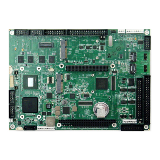
DSC-configurable default settings in battery-less configurations Initialize USB keyboard & mouse Customizable splash screen 5. BOARD LAYOUT The figure below shows the Hercules III board layout, including connectors, jumper blocks and mounting holes. JP10 JP11 SKT2 www.diamondsystems.com Hercules III User Manual Rev A.2... -
Page 17: Connector Summary
GPS PPS mSATA Socket PCIe MiniCard Socket SKT2 GPS Socket Jumper Summary The following table lists the jumper blocks on the Hercules III SBC. Jumper Description COM3 & COM4 RS-485/422 termination Digital I/O configuration LCD VDD select LCD backlight VDD select LCD scan direction and frame rate setting IRQ &... -
Page 18: Connectors
6. CONNECTORS This section describes the on-board Hercules III connectors. Note: All cables mentioned in this chapter are included in Diamond Systems’ cable kit C-HRCE-KIT. Some cables are also available individually. PC/104 ISA Bus (J1, J2) Connectors J1 and J2 carry the ISA bus signals. The following diagram shows the PC/104 A and B pin layout for J1 and the C and D pin layout for J2. -
Page 19: Pci-104 Bus (J3)
AD30 AD31 REQ0* REQ1* VI/O REQ2* GNT0* GNT1* VI/O GNT2* CLK0 CLK1 CLK2 CLK3 INTD* RST* +12V INTA* INTB* INTC* -12V Reserved Reserved GND/3.3V KEY SATA (J4) Industry standard vertical SATA connector. www.diamondsystems.com Hercules III User Manual Rev A.2 Page... -
Page 20: Utility (J7)
+5V In Ground Connector type: Shrouded .1” dual row straight pin header with gold flash plating Digital I/O (J8) Hercules III includes a 50-pin header, J8, for all digital I/O. J8 Digital I/O Connector DIO A0 DIO A1 DIO A2... - Page 21 (Output only! Do not connect to external supply) DGND Digital ground (0V - reference); used for digital circuitry only Diamond Systems cable number C-50-18 provides a standard 50-pin connector at each end and mates with this header. Connector type: Hirose DF50 1mm, RA, pos. lock, 50 pins www.diamondsystems.com...
-
Page 22: Analog I/O (J9)
Analog I/O (J9) Hercules III models with analog data acquisition include a 40-pin header, J9, for the analog I/O features. The pinout definition depends on the analog input jumper configuration. This is available only on models with data acquisition. Single-Ended... -
Page 23: Audio (J12)
Audio Ground Power Reference for Microphone Microphone Input Connector type: Vertical .1” pitch friction lock connector; Tyco 1-640456-0 or equivalent Diamond Systems cable number 6981025 mates with this header. Audio AMP (J13) Speaker Left + Volume Low Speaker Left -... -
Page 24: Serial Ports 1, 2, 3, 4 (J18)
RXD+ 4 Connector type: Standard 2.54mm dual row straight pin header with 4mm posts and gold flash plating Diamond Systems cable number C-DB9M-4 provides a standard DB9 connector at each end and mates with this header. 6.12 External Battery (J20) Connector J20 is used to connect an external battery for maintaining the real-time clock and CMOS settings (BIOS settings for various system configurations). -
Page 25: Usb (J21, J22)
10 USB0/2 VCC USB1/3 VCC Connectors J21 and J22 mate with Diamond Systems cable number 6981012, which provides two standard USB type A jacks in a panel-mount housing. Connector type: Standard 2.54mm dual row straight pin header with 4mm posts and gold flash plating 6.14 LCD Panel, LVDS Interface (J24) -
Page 26: Vga (J25)
GREEN signal (positive, 0.7Vpp into 75 Ohm load) Blue BLUE signal (positive, 0.7Vpp into 75 Ohm load) DDC clock/data Digital serial I/O signals used for monitor detection (DDC1 specification) HSYNC Horizontal sync VSYNC Vertical sync www.diamondsystems.com Hercules III User Manual Rev A.2 Page... -
Page 27: Serial Ports 5, 6 (J27)
Port 6 TXD 6 CTS 6 Diamond Systems cable number C-DB9M-2 provides a standard DB9 connector at each end and mates with this header. 6.17 LCD Backlight (J28) Connector J28 provides the backlight power and control for the optional LCD panel. See the description for connector J24, above, for details on the LCD data interface. -
Page 28: Can (J32)
Connector type: 1.25mm single row straight connector (Molex, LLC PN: 533980471 or equivalent and mating socket: Molex P/N510210400 or equivalent). Diamond Systems cable number 6981314 mates with this header. 6.19 Power Input (J29) Input power for Hercules III is supplied from a +7-40V external supply through connector J29 on pins +Vin. +Vin +Vin... -
Page 29: Msata (J35)
6.20 mSATA (J35) The mSATA connector is for cable-free connection to a SATA SSD module. The 52-pin mSATA connector supports mSATA modules. Signal Signal Pin# Name Name +3.3V +3.3V +3.3V +3.3V DA/DSS PRSNT# +3.3V www.diamondsystems.com Hercules III User Manual Rev A.2 Page... -
Page 30: Pcie Minicard (J36)
REFCLK+ UIM_RESET UIM_VPP Mechanical Key Reserved* (UIM_C8) Reserved* W_DISABLE# (UIM_C4) PERST# PERn0 +3.3Vaux PERp0 +1.5V SMB_CLK PETn0 SMB_DATA PETp0 USB_D- USB_D+ +3.3Vaux +3.3Vaux LED_WWAN# LED_WLAN# Reserved LED_WPAN# Reserved +1.5V Reserved Reserved +3.3Vaux www.diamondsystems.com Hercules III User Manual Rev A.2 Page... -
Page 31: Jumper Configuration
7. JUMPER CONFIGURATION The Hercules III board has the following jumper-selectable configuration options. Jumper Block Configuration Functions COM3 & COM4 RS-422/485 termination Digital I/O configuration LCD VDD select LCD backlight VDD select LCD scan direction and frame rate setting IRQ & FPGA address Selection... -
Page 32: Lcd Panel Configuration (Jp4, Jp5, Jp6)
7.3 LCD Panel Configuration (JP4, JP5, JP6) Hercules III has three jumpers that set the LCD configuration. JP4: LCD panel supply voltage +3.3V or +5V Pins Jumper installed Default No jumper +5V LCD VDD +3.3V LCD VDD Jumper JP5: LCD backlight power +5V or +12V (+12V provided through the input power connector) -
Page 33: Vio (Jp9)
Provides 47K pull up on RXD No jumper Provides 47K pull down on RTS No jumper Provides 47K pull up on DTR No jumper Provides 47K pull down on CTS No jumper www.diamondsystems.com Hercules III User Manual Rev A.2 Page... -
Page 34: System Operation
A serial port on another PC can be connected to the serial port on Hercules III with a null modem cable, and a terminal emulation program, such as HyperTerminal, can be used to establish the connection. The terminal program must be capable of transmitting special characters including F2 (some programs or configurations trap special characters). -
Page 35: Watchdog Timer
8. Exit the BIOS and save your settings. Watchdog Timer Hercules III contains a watchdog timer circuit provided by the Super I/O controller SCH3116. The watchdog timer can be configured using the BIOS and also using direct register command access mechanism to the SCH3116 controller. -
Page 36: System Reset
200 msec. 9. BIOS Hercules III uses a BIOS from American Megatrends modified to support the custom features of the SBC. BIOS Settings To change the following BIOS settings, press Del during system startup power on self-test (POST). -
Page 37: Miscellaneous Settings
The only power management mode supported by the system is “Power-On Suspend.” Other suspend modes are not supported and should not be used under any OS. Examples of unsupported suspend modes include, “Hibernate,” under Windows, and “Suspend-to-Disk” or “Suspend-to-RAM”. www.diamondsystems.com Hercules III User Manual Rev A.2 Page... -
Page 38: Bios Console Redirection Settings
The Ethernet chip is the Intel 82574 and Topcliff integrated MAC. The Hercules III Software CD includes Ethernet drivers for Windows XP, Windows CE, and Linux. The latest drivers can also be downloaded from National Semiconductor’s website, listed in the Additional Information section of this document. -
Page 39: Serial Ports
10.2 Serial Ports Hercules III contains six serial ports. Each port is capable of transmitting at speeds up to 115.2Kbaud. All ports are from the SCH3116 Super I/O chip. The serial ports use the following default system resources. Port I/O Address Range... -
Page 40: Operating Systems And Booting Procedures
3. Insert the DOS installation floppy disk into the USB floppy drive and start/restart the system. 4. Install any drivers needed. Note: For DOS Ethernet, set Operating System to other in the BIOS. Note: DOS Sound emulation is currently not functional. www.diamondsystems.com Hercules III User Manual Rev A.2 Page... -
Page 41: Data Acquisition Circuit
12. DATA ACQUISITION CIRCUIT Hercules III contains a data acquisition subsystem consisting of digital I/O (DIO), watchdog timer (WDC), counter/timer, pulse width modulation (PWM), and optional analog I/O features. The features of a board that includes data acquisition are equivalent to a complete PC/104 add-on data acquisition module. - Page 42 Figure 1: Data Acquisition Block Diagram www.diamondsystems.com Hercules III User Manual Rev A.2 Page...
- Page 43 Data Acquisition Circuitry I/O Map I/O Memory Space The data acquisition circuitry on Hercules III occupies a block of 32 bytes in I/O memory space. The default address range for this block is 0x240 – 0x24F (base address 0x240). The address range is a 32-byte block in ISA I/O Space. Within these 32-bytes, the registers are paged to provide full access to additional registers for additional functions;...
- Page 44 Page 3 is a 27-byte page occupying locations 1-27 of the chip, and contains a copyright notice in ASCII format. In page 3, the RESET command and page register at base + 0 are accessible, so the chip may be reset or the page changed. www.diamondsystems.com Hercules III User Manual Rev A.2 Page...
- Page 45 LOAD WDA7 WDA6 WDA5 WDA4 WDA3 WDA2 WDA1 WDA0 WDA15 WDA14 WDA13 WDA12 WDA11 WDA10 WDA9 WDA8 WDB7 WDB6 WDB5 WDB4 WDB3 WDB2 WDB1 WDB0 WDTRIG WDEN WDSMI WDRST WDT-1 WDEDGE WDIEN www.diamondsystems.com Hercules III User Manual Rev A.2 Page...
- Page 46 WDB0 Page 1 Write Offsets base+28, +29 and +31 refer to EEPROM Data, address, and unlock command registers for auto- calibration. Base + HOLDOFF RESET PAGE1 PAGE0 EE_EN EE_RW RUNCAL CMUXEN TDACEN www.diamondsystems.com Hercules III User Manual Rev A.2 Page...
- Page 47 ADQ1 ADQ0 FDID2 FDID1 FDID0 DAQ4 DAQ3 DAQ2 DAQ1 DAQ0 DIOQ7 DIOQ6 DIOQ5 DIOQ4 DIOQ3 DIOQ2 DIOQ1 DIOQ0 PWMQ3 PWMQ2 PWMQ1 PWMQ0 CTRQ3 CTRQ2 CTRQ1 CTRQ0 ID15 ID14 ID13 ID12 ID11 ID10 www.diamondsystems.com Hercules III User Manual Rev A.2 Page...
- Page 48 D/A output range: 0 = bipolar, 1 = unipolar. (Default on reset is unipolar mode). SEDIFF A/D mode: 0 = single-ended, 1 = differential. ADBU A/D input range: 0 = bipolar, 1 = unipolar. www.diamondsystems.com Hercules III User Manual Rev A.2 Page...
- Page 49 The A/D always works with a maximum input voltage of 10V. A gain of 2 means the maximum input voltage at the connector pin is 5V. 0 = gain of 1 1 = gain of 2 2 = gain of 4 3 = gain of 8 www.diamondsystems.com Hercules III User Manual Rev A.2 Page...
- Page 50 Base+6 and Base+7. The high-order bit determines if the data is transferred directly out to the DAC’s (transparent mode) or is latched and held for a later simultaneous update. D/A LSB: Base+6 (Write) Bit: Name: DA7-DA0 DA7-DA0 D/A LSB data. www.diamondsystems.com Hercules III User Manual Rev A.2 Page...
- Page 51 FIFO size, or 1024 samples. On power-up or system reset, the FIFO threshold is set to 1024 samples. FIFO Depth LSB: Base+10 (Read) Bit: Name: FD7-FD0 FD7-FD0 Current FIFO depth LSB. www.diamondsystems.com Hercules III User Manual Rev A.2 Page...
- Page 52 1 = external (J8, pin 41, EXTTRIG). CLKFRQ1 Internal clock frequency for counter 1: 0 = 10MHz 1 = 100 KHz CLKFRQ0 Internal clock frequency for counter 0: 0 = 10MHz 1 = 100 KHz www.diamondsystems.com Hercules III User Manual Rev A.2 Page...
- Page 53 A/D hardware clock enable. When CLKEN = 1, the A/D circuit is triggered by the hardware clock selected with CLKSEL above, and the software A/D trigger is disabled. 0 = disabled 1 = enabled www.diamondsystems.com Hercules III User Manual Rev A.2 Page...
- Page 54 ADSTART Start an A/D conversion. After this command, ADBUSY = 1, until the A/D conversion is finished. Each bit in this register represents a command. Writing a 1 to any bit executes the command specified by that bit. Only one bit may be written at a time. www.diamondsystems.com Hercules III User Manual Rev A.2 Page...
- Page 55 DIOB7-0 Port B DIO data. Digital I/O Port C: Base+18 (Read/Write) Bit: Name: DIOC7-0 DIOC7-0 Port C DIO data. Digital I/O Port D: Base+19 (Read/Write) Bit: Name: DIOD7-0 DIOD7-0 Port D DIO data. www.diamondsystems.com Hercules III User Manual Rev A.2 Page...
- Page 56 Direction for ports A – E. On power-up or system reset, all ports are set to input mode and the contents of the output registers are set to 0. 0 = input 1 = output www.diamondsystems.com Hercules III User Manual Rev A.2 Page...
- Page 57 Enable gating on selected counter. CTDIS Disable counting on selected counter. CTEN Enable counting on selected counter. LOAD Load selected counter with data in bytes 1-3 or 1-2, as appropriate. CLEAR Clear selected counter to zero. www.diamondsystems.com Hercules III User Manual Rev A.2 Page...
- Page 58 0 = rising edge. 1 = falling edge. WDIEN Enable external input hardware watchdog trigger instead of on-board software trigger. 0 = internal trigger only. 1 = external trigger plus internal trigger are enabled. www.diamondsystems.com Hercules III User Manual Rev A.2 Page...
- Page 59 2 = ID page 3 = Copyright notice page PWM Data LSB: Base+24 (Write) Bit: Name: PWMD7-0 PWMD7-0 PWM data bits 7-0. PWM Data CSB: Base+25 (Write) Bit: Name: PWMD15-8 PWMD15-8 PWM data bits 15-8. www.diamondsystems.com Hercules III User Manual Rev A.2 Page...
- Page 60 1 = enabled CTR/ENA If FLAG = 0, indicates which counter to act on: 0 = rate counter. 1 = duty cycle counter. If FLAG = 1, 0 = disabled 1 = running www.diamondsystems.com Hercules III User Manual Rev A.2 Page...
- Page 61 1 = enable calibration multiplexer and disable user analog input channels/muxes. TDACEN TrimDAC Enable. Setting this bit will initiates a transfer to the TrimDAC. This bit overrides the EE_EN setting; if both bits are set simultaneously, EE_EN is ignored. www.diamondsystems.com Hercules III User Manual Rev A.2 Page...
- Page 62 PAGE bit in order. This helps prevent accidental corruption of EEPROM contents. FPGA Revision Code: Base+31 (Read) Bit: Name: FPGA Revision Code FPGA This register indicates the revision number of the FPGA design. The current revision code is Revision 0x40. Code www.diamondsystems.com Hercules III User Manual Rev A.2 Page...
- Page 63 FDID2-0 Indicates the maximum sample depth supported by the FPGA FIFO. Currently, a value of “001” is defined, which describes a FIFO depth of 2048 samples. DAQ4-0 Indicates the number of D/A channels available on the board. www.diamondsystems.com Hercules III User Manual Rev A.2 Page...
- Page 64 Together with Chip ID LSB: Base+28, indicates the unique chip ID according to a (TBD) format. Each revision of the chip contains a unique 16-bit ID to enable software to distinguish between different board versions. The current chip ID should be 0x8000 or higher. www.diamondsystems.com Hercules III User Manual Rev A.2 Page...
- Page 65 1 = Extended features page 2 = ID page 3 = Copyright notice page Copyright Notice: Base+1 to Base+31 (Read) Bit: Name: Copyright Notice Text Copyright 31 bytes of 8-bit ASCII-formatted copyright notice text. Notice Text www.diamondsystems.com Hercules III User Manual Rev A.2 Page...
-
Page 66: Analog-To-Digital Input Ranges And Resolution
Overview Hercules III uses a 16-bit A/D converter. The full range of numerical values for a 16-bit number is 0 - 65535. However, the A/D converter uses two’s complement notation, so the A/D value is interpreted as a signed integer, ranging from –32768 to +32767. -
Page 67: Performing An A/D Conversion
A/D if AINTE = 0 (interrupts are disabled). When AINTE = 1, the A/D can only be triggered by the on- board counter/timer or an external signal. This protects against accidental triggering by software during a long- running interrupt-based acquisition process. outp(base,0x80); www.diamondsystems.com Hercules III User Manual Rev A.2 Page... -
Page 68: Wait For The Conversion To Finish
Since there are a large number of possible input devices, this secondary step is not included here. Only conversion to input voltage is described. However, you can combine both transformations into a single formula if desired. www.diamondsystems.com Hercules III User Manual Rev A.2 Page... -
Page 69: Conversion Formula For Bipolar Input Ranges
Input Voltage for 5V Range -32768 0.0000V -32767 1 LSB (V / 65536) 0.000076V / 2 - 1 LSB 2.4999V 2.5000V / 2 + 1 LSB 2.5001V 32767 - 1 LSB 4.9999V www.diamondsystems.com Hercules III User Manual Rev A.2 Page... -
Page 70: A/D Scan, Interrupt And Fifo Operation
The table on the next page describes the board’s behavior for each of the 4 possible cases of AINTE and SCANEN. The given interrupt software behavior describes the operation of the Diamond Systems Universal Driver software. If you write your own software or interrupt routine you should conform to the described behavior for optimum results. -
Page 71: Digital-To-Analog Output Ranges And Resolution
16.1 Description Hercules III uses a 4-channel 12-bit D/A converter (DAC) to provide four analog outputs. A 12-bit DAC can generate output voltages with the precision of a 12-bit binary number. The maximum value of a 12-bit binary number is 2 - 1, or 4095, so the full range of numerical values that the DACs support is 0 - 4095. -
Page 72: Resolution
In most cases, for unipolar mode configure the board to reset to zero scale, and for bipolar mode configure the board for reset to mid-scale. In each case, the DACs reset to 0V. www.diamondsystems.com Hercules III User Manual Rev A.2 Page... -
Page 73: D/A Conversion Formulas And Tables
Output Voltage for 0-10V Range 0.0000V 1 LSB (V / 4096) 0.0024V 2047 / 2 - 1 LSB 4.9976V 2048 5.0000V 2049 / 2 + 1 LSB 5.0024V 4095 - 1 LSB 9.9976V www.diamondsystems.com Hercules III User Manual Rev A.2 Page... -
Page 74: D/A Conversion Formulas For Bipolar Output Ranges
D/A Code Output Voltage Symbolic Formula Output Voltage for 10V Range -10.0000V + 1 LSB -9.9951V 2047 -1 LSB -0.0049V 2048 0.0000V 2049 +1 LSB 0.0049V 4095 - 1 LSB 9.9951V www.diamondsystems.com Hercules III User Manual Rev A.2 Page... -
Page 75: Generating An Analog Output
The status bit DACBUSY (Base+3, bit 4) indicates if the D/A is busy updating (1) or idle (0). After writing to the D/A, monitor DACBUSY until it is zero before continuing with the next D/A operation. www.diamondsystems.com Hercules III User Manual Rev A.2 Page... -
Page 76: Analog Circuit Calibration
18. ANALOG CIRCUIT CALIBRATION The Hercules III data acquisition circuit contains an advanced autocalibration circuit that can maintain the accuracy of both A/D and D/A circuits to within the specified tolerances regardless of time and temperature. Autocalibration is supported in the Diamond Systems Universal Driver software included with the board. -
Page 77: Digital I/O Operation
19. DIGITAL I/O OPERATION Hercules III contains 40 digital I/O lines organized as five 8-bit I/O ports: Port A-E. The direction of each port is programmable. Port E is also used for the PWM outputs. The port data are accessed at registers Base+16 through Base+20, and the port direction register is located at Base+22. -
Page 78: Counter/Timer Operation
20. COUNTER/TIMER OPERATION Hercules III contains two counter/timers that provide various timing functions on the board for A/D timing and user functions. These counters are controlled with registers in the on-board data acquisition controller FPGA. Counter 0 – A/D Sample Control 20.1... -
Page 79: Command Sequences
20.3 Command Sequences Diamond Systems provides driver software to control the counter/timers on Hercules III. The information in this section is intended as a guide for programmers writing their own code, instead of using the driver, and to give a better understanding of the counter/timer operation. -
Page 80: Disabling The Counter Gate Command
The value is returned in 3 bytes, low, middle, and high (2 bytes for counter 1). Counter 0: Counter 1: low=inp(base+12); low=inp(base+12); middle=inp(base+13); high=inp(base+13); high=inp(base+14); 23. Clear the counter. Counter 0: Counter 1: outp(base+15,0x01); outp(base+15,0x81); www.diamondsystems.com Hercules III User Manual Rev A.2 Page... -
Page 81: Watchdog Timer Programming
21. WATCHDOG TIMER PROGRAMMING Hercules III contains a watchdog timer circuit consisting of one programmable timer. The input to the circuit is WDI and the output is WDO, which appear on connector J8. WDI may be triggered in hardware or in software. A special “early”... - Page 82 0 = Watchdog timer counter disable, WDO disable, WDI disable, CPURST# disable, EXTSMI# disable. The CPLD initializes all values to zero on power up, and the BIOS enables each resource based on BIOS settings. www.diamondsystems.com Hercules III User Manual Rev A.2 Page...
-
Page 83: Data Acquisition Specifications
Counter/Timers (data acquisition units only) • A/D pacer clock: 24-bit down counter • Clock source: 10MHz, 1MHz or external signal • General purpose: 16-bit down counter • Clock source: 10MHz, 100KHz or external signal www.diamondsystems.com Hercules III User Manual Rev A.2 Page... -
Page 84: Msata Flashdisk Module
23. MSATA FLASHDISK MODULE Hercules III is designed to accommodate an optional solid-state mSATA flashdisk module using either MLC (FDMM-xxG-XT models) or SLC (FDMS-xxG-XT models) technology. The modules contain from 8GB to 64GB of solid-state non-volatile memory that operates like a disk drive without requiring additional driver software support. -
Page 85: Specifications
Analog Outputs: 4, 12-bit resolution • Output ranges: ±5V, ±10V, 0-5V, 0-10V • Output current: ±5mA max per channel • Settling time: 7µS max to 0.01% • Relative accuracy: ±1 LSB • Nonlinearity: ±1 LSB, monotonic www.diamondsystems.com Hercules III User Manual Rev A.2 Page... -
Page 86: Power Supply
Available Power: 35W (up to 20W consumed by SBC) 24.4 General • Shock: MIL-STD-202G, Method 213B compliant • Vibration: MIL-STD-202G, Method 214A compliant • Dimensions: 5.75 x 8.0 in. (106 x 114mm) • Weight: 10.1oz.(286g) without heatsink www.diamondsystems.com Hercules III User Manual Rev A.2 Page...
Need help?
Do you have a question about the Hercules III and is the answer not in the manual?
Questions and answers