Table of Contents
Advertisement
Quick Links
Advertisement
Table of Contents

Related Manuals for Diamond Systems Athena II


Summary of Contents for Diamond Systems Athena II
- Page 1 Athena II User Manual High Integration SBC with Ethernet and Data Acquisition User Manual v1.00 © Copyright 2008 Diamond Systems Corporation 1255 Terra Bella Ave. Mountain View, CA 94043 Tel (650) 810-2500 Fax (650) 810-2525 www.diamondsystems.com...
-
Page 2: Table Of Contents
IDE (J8)........................23 External Battery (J9)....................24 Input Power (J11).....................25 External Auxiliary Power, Output (J12)..............26 Data Acquisition, Digital I/O (J14)................27 Speaker (J15)......................28 Auto-Calibration Reference Voltage (J17)...............29 LCD Panel, LVDS Interface (J24)................29 VGA (J25)........................30 Diamond Systems Corporation Athena II User Manual Page 2... - Page 3 Notes on Operating Systems and Booting Procedures..........48 Windows Operating System Installation Issues............48 Driver Installation....................48 BIOS Setting for Windows...................48 CompactFlash Under Windows................48 DOS Operating Systems Installation Issues............48 CompactFlash Compatibility Issues Under DOS.............48 Data Acquisition Circuit....................50 Diamond Systems Corporation Athena II User Manual Page 3...
- Page 4 Write the Value to the Selected Output Channel Registers........80 Wait for the D/A to Update..................81 Analog Circuit Calibration....................82 A/D Bipolar Offset....................82 A/D Unipolar Offset....................82 A/D Full-scale......................82 D/A Full-scale......................82 Digital I/O Operation......................83 Diamond Systems Corporation Athena II User Manual Page 4...
- Page 5 IDE Configuration.....................95 Booting into MS-DOS, FreeDOS or ROM-DOS............96 Booting into Linux or Microsoft Windows..............96 Specifications.........................97 CPU..........................97 Data Acquisition Circuitry..................97 Power Supply......................98 General........................98 Additional Information....................99 Appendix A – BIOS CMOS Option Listing..............100 Diamond Systems Corporation Athena II User Manual Page 5...
- Page 6 Security......................110 Power.........................111 Boot........................111 Technical Support......................112 Figures Figure 1: Athena II Block Diagram...................11 Figure 2: Athena II Board Layout..................15 Figure 3: J3 Main I/O Connector..................18 Figure 4: J4 Ethernet Connector..................21 Figure 5: J5/J21 USB Connectors...................21 Figure 6: J6 Watchdog Timer Access Connector............22 Figure 7: J7 USB0 Connector (end view)................23...
- Page 7 Figure 26: Analog Output Configuration Selection............38 Figure 27: J18 Jumper Block...................38 Figure 28: Watchdog Timer Block Diagram..............40 Figure 29: Athena II Data Acquisition Block Diagram.............50 Figure 30: FlashDisk Module...................91 Figure 31: FlashDisk Programmer Board Layout............93 Figure 32: Cable Kit C-ATH-KIT..................94...
-
Page 8: Introduction
256MB The Athena II CPU uses the ISA bus, internally, to connect serial ports 1 through 4 and the data acquisition circuit to the processor. The ISA bus is brought out to an expansion connector to mate with add-on boards. Diamond Systems Corporation manufactures a wide variety of compatible PC/104 add-on boards for analog I/O, digital I/O, counter/timer functions, serial ports and power supplies. -
Page 9: Analog Input
1 24-bit counter/timer for A/D sampling rate control. • 1 16-bit counter/timer for user counting and timing functions. • Programmable gate and count enable. • Internal and external clocking capability. • System Features Diamond Systems Corporation Athena II User Manual Page 9... - Page 10 • ATX power switching capability. • Programmable watchdog timer. • Power supply: 5VDC operation from the PC/104 bus or a power connector. • Extended temperature range operation: -40 to +85°C. • Diamond Systems Corporation Athena II User Manual Page 10...
-
Page 11: Block Diagram
Block Diagram Figure 1 shows the Athena II functional blocks. Figure 1: Athena II Block Diagram Diamond Systems Corporation Athena II User Manual Page 11... -
Page 12: Functional Overview
Functional Overview This section describes the major Athena II subsystems. Processor The board uses the VIA Mark integrated processor, with integrated Northbridge, up to the rated processor speed of 500/800MHz. An appropriate heat sink is required, depending on the processor speed. The design supports a 5VDC fan with speed sensing. -
Page 13: Data Acquisition
IDE ports One 44-pin connector for HDD or compact flashdisk socket Athena II contains four serial ports. Each port is capable of transmitting at speeds of up to 115.2Kbaud, and uses a dedicated RS-232 transceiver with ESD protection. Ports COM1 and COM2 are built into the standard chipset, consisting of standard 16550-type UARTs with 16-byte FIFOs. -
Page 14: Power Supply
Note: The ATX power switch does not control the master +5V on the board. Battery Backup Athena II contains a backup battery for the real-time clock and BIOS settings. The battery is directly soldered to the board and provides a minimum 7 year backup lifetime at 25oC. -
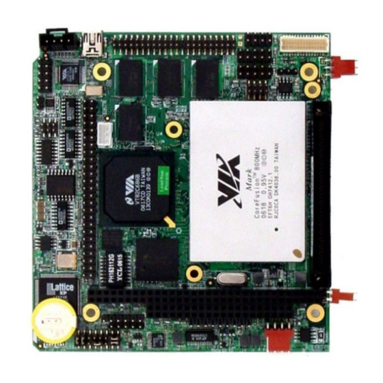
Page 15: Board Description
Board Description Board Layout Figure 2 shows the Athena II board layout, including connectors, jumper blocks and mounting holes. Figure 2: Athena II Board Layout Diamond Systems Corporation Athena II User Manual Page 15... -
Page 16: Connector Summary
Connector Summary The following table lists the connectors on the Athena II board. Connector Description PC/104, ISA bus A,B PC/104, ISA bus C,D Main I/O (serial ports, PS/2 keyboard/mouse, parallel port, utility) Ethernet USB 0/1 Watchdog/Failsafe Features USB0 (mini-USB connector) -
Page 17: Connectors
Connectors This section describes the on-board Athena II connectors. Note: All cables mentioned in this chapter are included in Diamond Systems’ cable kit C-ATH-KIT. Some cables are also available individually. PC/104 ISA Bus (J1, J2) Connectors J1 and J2 carry the ISA bus signals. The following diagram shows the PC/104 A and B pin layout for J1 and the C and D pin layout for J2. -
Page 18: Figure 3: J3 Main I/O Connector
PS/2 keyboard • PS/2 mouse • IrDA port • ATX Power switch • Reset switch • Power and HDD LEDs • Figure 3: J3 Main I/O Connector Diamond Systems Corporation Athena II User Manual Page 18... - Page 19 GND 36 36 ATX Power Utilities A +5V Out 37 37 KB Lock Speaker Out 38 38 IR RX IDE Drive LED 39 39 IR TX Power LED 40 40 +3VSB Diamond Systems Corporation Athena II User Manual Page 19...
- Page 20 Connector J3 mates with Diamond Systems Corporation cable no. C-PRZ-01, which consists of a dual-ribbon-cable assembly with industry-standard connectors at the user end. The CPU mating connector includes integral latches for enhanced reliability.
-
Page 21: Ethernet (J4)
Ethernet (J4) Ethernet connectivity is provided by 1x6-pin connector J4. Connector J4 mates with Diamond Systems Corporation cable no. 698002, which provides a panel-mount RJ-45 jack for connection to standard CAT5 network cables. Figure 4: J4 Ethernet Connector Common Common USB (J5, J21) Connectors J5 (USB 0/1) and J21 (USB 2/3) provide four USB 2.0 ports. -
Page 22: Watchdog Timer (J6)
Data - Ground Connectors J5 and J21 mate with Diamond Systems Corporation cable no. 698012, which provides two standard USB type A jacks in a panel-mount housing. Note: USB0 (J7) shares the J5 USB circuitry. Do not connect USB devices to both USB0 and J5. -
Page 23: Ide (J8)
Note: USB0 shares the J5 USB circuitry. Do not connect USB devices to both USB0 and J5. IDE (J8) Connector J8 is a 2x22-pin header used for an IDE connection. An associated mounting hole is provided to install a flash disk module. Figure 8: J8 IDE Connector Diamond Systems Corporation Athena II User Manual Page 23... -
Page 24: External Battery (J9)
Ground Not used Connector J8 mates with Diamond Systems Corporation cable no. 698004, and may be used to connect up to two IDE drives (hard disks, CD-ROMs, or flash disk modules). The 44-pin connector includes power and mates directly with notebook drives and flash disk modules. To use a standard format hard disk or CD-ROM drive with a 40-pin connector, an adapter PCB such as Diamond Systems CorporationACC-IDEEXT is required. -
Page 25: Input Power (J11)
Ground Input Power (J11) Input power for Athena II may be supplied either from an external supply, through J11, or directly through the PC/104 bus power pins if a PC/104 power supply is used with the CPU. Figure 10: J11 Input Power Connector... -
Page 26: External Auxiliary Power, Output (J12)
4 seconds or longer will turn off power. Diamond Systems’ cable no. 698009 mates with J11. It provides 9 color-coded wires with stripped and tinned leads for connection to user-supplied power sources. -
Page 27: Data Acquisition, Digital I/O (J14)
Data Acquisition, Digital I/O (J14) Athena II includes a 50-pin header, J14, for all data acquisition I/O. Figure 12: J14 Digital I/O Connector DIO A0 DIO A1 DIO A2 DIO A3 DIO A4 DIO A5 DIO A6 DIO A7 DIO B0... -
Page 28: Speaker (J15)
Analog ground; used for analog circuitry only. Vout pin is for analog outputs, Vin pin is for analog inputs. Diamond Systems Corporation cable no. C-50-18 provides a standard 50-pin connector at each end and mates with this header. Speaker (J15) Connector J15 is a 2x5-pin header used to connect speakers. -
Page 29: Auto-Calibration Reference Voltage (J17)
Connector J17 is a two-pin header used for auto-calibration. AutoCal Reference Value The Diamond Systems Corporation AutoCal routines read the exact voltage calibration values from the AutoCal- Flash. There are four analog values that need to be measured and stored in the AutoCal flash during manufacturing test. -
Page 30: Vga (J25)
+3.3V Switched Power Supply for LCD display (only powered up when LCD display is active) Ground Power Ground, 0V VGA (J25) Connector J25 is a 2x4-pin header for connecting a VGA monitor. Figure 15: J25 VGA Connector Green Blue Ground Diamond Systems Corporation Athena II User Manual Page 30... -
Page 31: Cpu Fan (J27)
Note: While the DDC serial detection pins are present, a 5V power supply is not provided (the old “Monitor ID” pins are also not used). Diamond Systems Corporation Cable Assembly 698024 provides a female DB15 connection to interface with a standard RGB monitor. -
Page 32: Cd Input (J30)
+12V Power supply for LCD Backlight assembly Control Output signal (from Athena II) to allow power-down of backlight Ground Ground for LCD Backlight assembly Connector J28 provides the backlight power and control for the optional LCD panel. See the description for connector J24, above, for details on the LCD data interface. - Page 33 The connector is an industry-standard CD-IN connector, which is common in most desktop Personal Computers. Note that the left and right grounds are decoupled but are also tied together on-board. This input is intended for CD- input only; i.e., no amplified or microphone inputs. Diamond Systems Corporation Athena II User Manual Page 33...
-
Page 34: Board Configuration
Board Configuration The Athena II board has the following jumper-selectable configuration options. Note: Connector J10 is not installed on the standard Athena II board. Jumper Block Configuration Functions System configuration jumper block. Data acquisition circuit configuration jumper block. RS-485 mode selection jumper block. -
Page 35: Serial Port And A/D Irq Settings
IRQ at a time; the ability for all three devices to run simultaneously is not supported. Configure the IRQ options as shown in the following jumper settings. Figure 20: IRQ Configuration Options Diamond Systems Corporation Athena II User Manual Page 35... -
Page 36: Erasing Cmos Ram Settings
If the ATX jumper is removed, the battery-backup for CMOS does not function when power is removed. DAC Configuration (J13) Jumper block J13 is used to configure the A/D and D/A circuits. Figure 23: J13 Jumper Block Diamond Systems Corporation Athena II User Manual Page 36... -
Page 37: Single-Ended/Differential Input Settings
Differential inputs are frequently used either when the grounds of the input device and the measurement device (Athena II) are at different voltages, or when a low-level signal is being measured that has its own ground wire. A differential input also has higher noise immunity than a single-ended input because most noise affects both (+) and (–) input wires equally, so the noise is canceled out in the measurement. -
Page 38: Mode Selection (J18)
Jumper block J18 is used to select RS-485 mode for COM3/COM4. Figure 27: J18 Jumper Block Note 1. RS-485 mode needs to be set in the BIOS. Note 2. Echo is enabled when RS-485 is set in half-duplex mode. Diamond Systems Corporation Athena II User Manual Page 38... -
Page 39: System Operation
A serial port on another PC can be connected to the serial port on Athena II with a null modem cable, and a terminal emulation program, such as HyperTerminal, can be used to establish the connection. -
Page 40: Watchdog Timer
Watchdog Timer Athena II contains a watchdog timer circuit consisting of two programmable timers, WD1 and WD2, cascaded together. The input to the circuit is WDI and the output is WDO. WDI may be triggered in hardware or in software. -
Page 41: Flash Memory
The WD2 timer gives external circuits time to respond to the WDO event before the hardware reset occurs. The watchdog timer circuit is programmed via I/O registers located on Page 0: Base +28-31. The Athena II watchdog timer is supported in the Diamond Systems Corporation Universal Driver software version 5.7 and later. -
Page 42: On-Board Video
200 msec. On-Board Video Using the the on-board VIA Mark processor, Athena II integrates all of the support needed for modern media. Refer to the VIA Technologies, Inc. documentation for the Mark processor, listed in the Additional Information section of this document. -
Page 43: Bios
The Frame Buffer size can be increased for specific applications. Be aware, however, that an increase in this memory size will result in a decrease in overall system memory available. The AGP rate affects internal video accesses and does not affect any external bus speeds. Diamond Systems Corporation Athena II User Manual Page 43... -
Page 44: Bios Console Redirection Settings
Console Type: PC ANSI (default), VT100, VT100 (8-bit), PC-ANSI (7-bit), VT100+, or VT-UTF8. • Flow Control: CTS/RTS (default), XON-XOFF, None. • Number of video Pages to support: 1(default) to 8. • Diamond Systems Corporation Athena II User Manual Page 44... - Page 45 Note: Console Redirection only works for text-based interaction. If the OS enables video and starts using direct video functions (which would be the case with a Linux X-terminal or Windows, for example), Console Redirection has no effect and video is then required. Diamond Systems Corporation Athena II User Manual Page 45...
-
Page 46: System I/O
Additional software support includes a packet driver with software to allow a full TCP/IP implementation. Serial Ports Athena II contains four serial ports. Each port is capable of transmitting at speeds up to 115.2Kbaud. Ports COM1 and COM2 are built into the standard chipset., which are standard 16550 UARTs with 16-byte FIFOs. -
Page 47: Usb Ports
The BIOS supports the USB keyboard during BIOS initialization screens and legacy emulation for DOS-based applications. The USB ports can be used for keyboard and mouse at the same time that the PS/2 keyboard and mouse are connected. Diamond Systems Corporation Athena II User Manual Page 47... -
Page 48: Notes On Operating Systems And Booting Procedures
1. For DOS Ethernet, set Operating System to other in the BIOS. 2. DOS Sound emulation is currently not functional. CompactFlash Compatibility Issues Under DOS CompactFlash is incompatible with some utilities, under some versions of DOS. CompactFlash with ROM-DOS • Diamond Systems Corporation Athena II User Manual Page 48... - Page 49 CompactFlash. with MS-DOS CompactFlash • The MS-DOS FDISK, FORMAT, and SYS utilities are not functional when used with CompactFlash. The MS- DOS operating system files cannot be installed on CompactFlash flash. Diamond Systems Corporation Athena II User Manual Page 49...
-
Page 50: Data Acquisition Circuit
Data Acquisition Circuit Athena II contains a data acquisition subsystem consisting of A/D, D/A, digital I/O, and counter/timer features. This subsystem is equivalent to a complete add-on data acquisition module. The A/D section includes a 16-bit A/D converter, 16 input channels, and a 48-sample FIFO. Input ranges are programmable, and the maximum sampling rate is 100KHz. -
Page 51: Data Acquisition Circuitry I/O Map
Data Acquisition Circuitry I/O Map Overview The data acquisition circuitry on Athena II occupies 16 bytes in I/O memory space. The default address range is 280h (base address) to 28Fh. The data acquisition FPGA can be enabled/disabled in the BIOS under the Advanced menu. Scroll down to the “FPGA Mode”... -
Page 52: Register Map Bit Summary
SCANEN CKSEL1 CKFRQ1 CKFRQ0 ADCLK DMAEN TINTE DINTE AINTE FD5-FD0 DMAINT TINT DINT AINT ADCH3 ADCH2 ADCH1 ADCH0 DIOCTR DIRA DIRCH DIRB DIRCL REV7 REV6 REV5 REV4 REV3 REV2 REV1 REV0 Diamond Systems Corporation Athena II User Manual Page 52... - Page 53 EEM_D7-EEM_D0 EEM_CA7-EEM_CA0 TDABSY EEMBSY ADCMEN PG1ID Page 2 Write Register Summary Base + ADCEXF UNIBIDI UNIBIOE SEDIFDI SEDIFOE Page 2 Read Register Summary Base + ADCEXF UNIBIDI UNIBIOE SEDIFDI SEDIFOE PG2ID Diamond Systems Corporation Athena II User Manual Page 53...
-
Page 54: Page 0 Register Definitions
The user’s interrupt routine must write to the appropriate bit prior to exiting to reset the interrupt request • flip flop, enabling future interrupts. Otherwise, the interrupt line remains high, indefinitely, and no additional interrupt requests are generated by the board. Diamond Systems Corporation Athena II User Manual Page 54... - Page 55 AD15-AD8 A/D MSB data. The A/D data must be read LSB first, followed by MSB. (Refer to the method for deriving the A/D value described in the Base+0 (Read) description, above.) Diamond Systems Corporation Athena II User Manual Page 55...
- Page 56 …. Reading from this register returns the value previously written to it. • Analog Input Gain/Page Select/Scan Settings: Base+3 (Write) Bit: Name: SCANEN PG1-PG0 Page select (Page 0 - Page 2) Diamond Systems Corporation Athena II User Manual Page 56...
- Page 57 A/D conversion. The following table lists the possible analog input ranges. • Gain Unipolar Range Bipolar Range Invalid ±10V 0 - 8.3V ±5V 0 - 5 V ±2.5V 0 - 2.5V ±1.25V Diamond Systems Corporation Athena II User Manual Page 57...
- Page 58 5V. 0 = gain of 1 1 = gain of 2 2 = gain of 4 3 = gain of 8 (See the description for register Base+3, write, above). Diamond Systems Corporation Athena II User Manual Page 58...
- Page 59 The user’s interrupt routine must monitor the status bits to know which circuit has requested service. After processing the data but before exiting, the interrupt routine must clear the appropriate interrupt request bit, using the Base+0 register. Diamond Systems Corporation Athena II User Manual Page 59...
- Page 60 Base+7 immediately updates the DAC. A/D Channel and FIFO Status: Base+6 (Read) Bit: Name: FD5-FD0 FD5-FD0 Current FIFO depth. This value indicates the number of A/D values currently stored in the FIFO. Diamond Systems Corporation Athena II User Manual Page 60...
- Page 61 When any of bits 7–4 are 1, the corresponding circuit is requesting service. The interrupt routine must poll • these bits to determine which circuit needs service and then act accordingly. Diamond Systems Corporation Athena II User Manual Page 61...
- Page 62 Port B data. The register direction is controlled by bits in the register Base+11, below. Digital I/O Port C: Base+10 (Read/Write) Bit: Name: C0-C7 Port Cdata. The register direction is controlled by bits in the register Base+11, below. Diamond Systems Corporation Athena II User Manual Page 62...
- Page 63 Base+15, the selected counter’s LSB register is loaded with this value. When reading from this register, the LSB value of the most recent Latch command is returned. Note: The value returned is NOT the value written to this register. Diamond Systems Corporation Athena II User Manual Page 63...
- Page 64 When reading from this register, the MSB value of the most recent Latch command for counter 0 is returned. Note: The value returned is NOT the value written to this register. Diamond Systems Corporation Athena II User Manual Page 64...
- Page 65 FPGA Revision Code: Base+15 (Read) Bit: Name: REV7 REV6 REV5 REV4 REV3 REV2 REV1 REV0 REV0-7 Revision code, read as a two-digit hexadecimal value. For example, a value of 0x20 is revision 2.0 Diamond Systems Corporation Athena II User Manual Page 65...
-
Page 66: Page 1 Register Definitions
Data for the command data for the EEPROM. Data can only be written when EEMBSY (base+14) is EEM_CD0 cleared. EEM Data: Base+12 (Read) Bit: Name: EEM_D7-EEM_D0 EEM_D7- EEM data pointed to by EEPROM command address register (base+13). EEM_D0 Diamond Systems Corporation Athena II User Manual Page 66... - Page 67 TrimDAC address can be written by writing to this register or through the EEM mode (). TrimDAC data can only be written when TDABSY (base+14) is not set. Reset value is zero. EEM Command Address: Base+13 (Read) Bit: Name: EEM_CA7-EEM_CA0 EEM_CA7- EEPROM command address. EEM_CA0 Diamond Systems Corporation Athena II User Manual Page 67...
- Page 68 Write Enable: Base+15 (Write) Bit: Name: WREN7-WREN0 WREN7/0 EEPROM write enable. Write the value 0xA5 before starting an EEPROM write command. Note: This register can only be written when EEMBSY (base+14) is cleared. Diamond Systems Corporation Athena II User Manual Page 68...
-
Page 69: Page 2 Register Definitions
Output enable. When set, the SEDIFDI value is gated to the output. Page 2 Select Read Back Check: Base+15 (Read) Bit: Name: PG2ID PGID Register page 2 ID. This register always contains the value 0xA2. Diamond Systems Corporation Athena II User Manual Page 69... -
Page 70: Analog-To-Digital Input Ranges And Resolution
Overview Athena II uses a 16-bit A/D converter. The full range of numerical values for a 16-bit number is 0 - 65535. However, the A/D converter uses two’s complement notation, so the A/D value is interpreted as a signed integer, ranging from –32768 to +32767. -
Page 71: Performing An A/D Conversion
Monitor the WAIT bit at Base+3, bit 5. When the bit value is 1, the circuit is actively settling on the input signal. When the value is 0, the board is ready to perform A/D conversions. Perform an A/D Conversion on the Current Channel Diamond Systems Corporation Athena II User Manual Page 71... -
Page 72: Wait For The Conversion To Finish
FIFO. The FIFO depth register increments by the scan size. When STS goes low, the program should read out the data for all channels. Diamond Systems Corporation Athena II User Manual Page 72... -
Page 73: Convert The Numerical Data To A Meaningful Value
A/D Code Input Voltage Symbolic Formula Input Voltage for ± 5V Range -32768 -5.0000V -32767 + 1 LSB -4.9998V -1 LSB -0.00015V 0.0000V +1 LSB 0.00015V 32767 - 1 LSB 4.9998V Diamond Systems Corporation Athena II User Manual Page 73... -
Page 74: Conversion Formula For Unipolar Input Ranges
A/D Code Input Voltage Symbolic Formula Input Voltage for 0− 5V Range -32768 0.0000V -32767 1 LSB (V / 65536) 0.000076V / 2 - 1 LSB 2.4999V 2.5000V / 2 + 1 LSB 2.5001V 32767 - 1 LSB 4.9999V Diamond Systems Corporation Athena II User Manual Page 74... -
Page 75: A/D Scan, Interrupt And Fifo Operation
The table on the next page describes the board’s behavior for each of the 4 possible cases of AINTE and SCANEN. The given interrupt software behavior describes the operation of the Diamond Systems Universal Driver software. If you write your own software or interrupt routine you should conform to the described behavior for optimum results. - Page 76 STS stays high during the entire scan (multiple A/D conversions). A/D interrupt occurs when the FIFO reaches its programmed threshold. The interrupt routine reads the number of samples equal to the FIFO threshold (Base+5, bits 0-5). Diamond Systems Corporation Athena II User Manual Page 76...
-
Page 77: Digital-To-Analog Output Ranges And Resolution
Description Athena II uses a 4-channel 12-bit D/A converter (DAC) to provide four analog outputs. A 12-bit DAC can generate output voltages with the precision of a 12-bit binary number. The maximum value of a 12-bit binary number is 2 1, or 4095, so the full range of numerical values that the DACs support is 0 - 4095. -
Page 78: D/A Conversion Formulas For Unipolar Output Ranges
D/A Code Output Voltage Symbolic Formula Output Voltage for 0-10V Range 0.0000V 1 LSB (V / 4096) 0.0024V 2047 / 2 - 1 LSB 4.9976V 2048 5.0000V 2049 / 2 + 1 LSB 5.0024V 4095 - 1 LSB 9.9976V Diamond Systems Corporation Athena II User Manual Page 78... -
Page 79: D/A Conversion Formulas For Bipolar Output Ranges
D/A Code Output Voltage Symbolic Formula Output Voltage for ± 10V Range -10.0000V + 1 LSB -9.9951V 2047 -1 LSB -0.0049V 2048 0.0000V 2049 +1 LSB 0.0049V 4095 - 1 LSB 9.9951V Diamond Systems Corporation Athena II User Manual Page 79... -
Page 80: Generating An Analog Output
Write these values to the selected channel. The LSB is written to Base+6. The MSB and channel number are written to Base+7 (MSB = bits 0-3, channel number,0-3 = bits 6-7). outp(Base+6, LSB); outp(Base+7, MSB + channel << 6); Diamond Systems Corporation Athena II User Manual Page 80... -
Page 81: Wait For The D/A To Update
The status bit DACBUSY (Base+3, bit 4) indicates if the D/A is busy updating (1) or idle (0). After writing to the D/A, monitor DACBUSY until it is zero before continuing with the next D/A operation. Diamond Systems Corporation Athena II User Manual Page 81... -
Page 82: Analog Circuit Calibration
The analog I/O circuit is calibrated during production test prior to shipment. Over time the circuit may drift slightly. If calibration is desired, internal auto-calibration can be performed using the software routines provided with the Diamond Systems Corporation driver libraries, which are included with the Athena II development kit. Four adjustments are possible: A/D bipolar offset. -
Page 83: Digital I/O Operation
Digital I/O Operation Athena II contains 24 digital I/O lines organized as three 8-bit I/O ports: Port A, Port B, and Port C. The direction of each port is programmable, and port C is further divided into two 4-bit halves, each with independent direction. -
Page 84: Counter/Timer Operation
Counter/Timer Operation Athena II contains two counter/timers that provide various timing functions on the board for A/D timing and user functions. These counters are controlled with registers in the on-board data acquisition controller FPGA. Counter 0 – A/D Sample Control Counter 0 is a 24-bit, “divide-by-n”... -
Page 85: Command Sequences
Command Sequences Diamond Systems provides driver software to control the counter/timers on Athena II. The information in this section is intended as a guide for programmers writing their own code, instead of using the driver, and to give a better understanding of the counter/timer operation. -
Page 86: Disabling The Counter Gate Command
The value is returned in 3 bytes, low, middle, and high (2 bytes for counter 1). Counter 0: Counter 1: low=inp(base+12); low=inp(base+12); middle=inp(base+13); high=inp(base+13); high=inp(base+14); 3. Clear the counter. Counter 0: Counter 1: outp(base+15,0x01); outp(base+15,0x81); Diamond Systems Corporation Athena II User Manual Page 86... -
Page 87: Watchdog Timer Programming
Watchdog Timer Programming Athena II contains a watchdog timer circuit consisting of one programmable timer. The input to the circuit is WDI and the output is WDO, which appear on connector J6. WDI may be triggered in hardware or in software. A special “early”... -
Page 88: Example: Watchdog Timer With Software Trigger
A software trigger relies on a thread of execution to constantly trigger watchdog timer A. If the thread is ever halted, timer A decrements to zero and starts timer B. Once timer B decrements to 0, the board resets. Diamond Systems Corporation Athena II User Manual Page 88... -
Page 89: Example: Watchdog Timer With Hardware Trigger
When timer A reaches 1, a rising edge flows from WDO to WDI, resetting the timer back to 100 and lowering WDO. When the connection from WDO to WDI is broken, the rising edge never reaches WDI and system resets. Diamond Systems Corporation Athena II User Manual Page 89... -
Page 90: Data Acquisition Specifications (Data Acquisition Units Only)
• Counter/Timers A/D pacer clock: 24-bit down counter • Clock source: 10MHz, 1MHz or external signal • General purpose: 16-bit down counter • Clock source: 10MHz, 100KHz or external signal • Diamond Systems Corporation Athena II User Manual Page 90... -
Page 91: Flashdisk Module
FlashDisk Module Athena II is designed to accommodate an optional solid-state FlashDisk module. This module contains 32MB to 128MB of solid-state non-volatile memory that operates like an IDE drive without requiring additional driver software support. Model Capacity FD-32-XT 32MB FD-64-XT... -
Page 92: Using The Flashdisk With Another Ide Drive
The power may be provided from the CPU’s power out connector, J12, or from one of the two 4-pin headers on the ACC-IDEEXT board. Athena II cable no. 698006 may be used with either power connector to bring power to the drive. -
Page 93: Flashdisk Programmer Board
The board can also be used to enable the simultaneous connection of two drives to the CPU. Connector J1 connects to the IDE connector on Athena II with a 44-pin ribbon cable (Diamond Systems Corporation part no. 698004). Both 40-pin .1-inch spacing, J4, and 44-pin 2mm spacing, J3, headers are provided for the external hard drive or CD-ROM drive. -
Page 94: I/O Cables
I/O Cables Diamond Systems Corporation offers cable kit C-ATH-KIT with ten cables to connect to all I/O headers on the board, shown in Figure 32. Some cables are also available separately. Figure 32: Cable Kit C-ATH-KIT Photo No. Cable No. -
Page 95: Quick Start Guide
Quick Start Guide This section describes the steps needed to get your Athena II board up and running, and assumes that you have also purchased the Athena Development Kit. The development kit includes all cables described in the previous section, a power supply, USB floppy drive, mounting hardware, IDE flashdisk and the flashdisk programmer board. -
Page 96: Booting Into Ms-Dos, Freedos Or Rom-Dos
2. Insert your DOS-based boot disk into the USB floppy drive. 3. Connect the power supply to the wall (to provide power to Athena II). 4. At this point the Athena II will boot and you should see the BIOS power-on self test. Press F2 to enter BIOS configuration. -
Page 97: Specifications
Output current: Logic 0: 64mA max per lineLogic 1: -15mA max per line • A/D Pacer clock: 24-bit down counter (source: 10MHz, 1MHz or external signal) • General purpose: 16-bit down counter (source: 10MHz, 100KHz or external signal) • Diamond Systems Corporation Athena II User Manual Page 97... -
Page 98: Power Supply
Power Supply Input Voltage: +5VDC ±5% • General Dimensions: 4.528” x 6.496” (115mm x 165mm) • Weight: TBD • Diamond Systems Corporation Athena II User Manual Page 98... -
Page 99: Additional Information
Additional Information Additional information can be found at the following websites. 1. Diamond Systems Corporation: http://www.diamondsystems.com/ 2. VIA Technologies, Inc.: http://www.via.com.tw/en/products/processors/corefusion/mark/index.jsp 3. National Semiconductor Corporation: http://www.national.com Diamond Systems Corporation Athena II User Manual Page 99... -
Page 100: Appendix A - Bios Cmos Option Listing
Load default BIOS settings, without exiting BIOS setup mode. Discard Changes Discard any changes made, without exiting BIOS setup mode. Save Changes Save any changes made, without exiting BIOS setup mode. Diamond Systems Corporation Athena II User Manual Page 100... -
Page 101: Bios Screen Descriptions
Memory Cache See Memory Cache Setup. Quick Boot Mode ENABLED DISABLED - Floppy Check DISABLED ENABLED System Summary Screen DISABLED ENABLED System Memory 640KB Extended Memory xxxxxxxKB Determined by the BIOS. Diamond Systems Corporation Athena II User Manual Page 101... - Page 102 This screen is the same as the Primary Master HDD Setup screen. Memory Shadow Default Value Change Optional Configuration Item Comments Values User Entry Allowed System shadow Enabled Video shadow Enabled Disabled Diamond Systems Corporation Athena II User Manual Page 102...
- Page 103 Cache C800-CBFF Disabled Write-Protect Write-Back USWC Write-Through Cache CC00-CFFF Disabled Write-Protect Write-Back USWC Write-Through Cache D000-D3FF Disabled Write-Protect Write-Back USWC Write-Through Cache D400-D7FF Disabled Write-Protect Write-Back USWC Cache D800-DBFF Disabled Write-Through Write-Protect Diamond Systems Corporation Athena II User Manual Page 103...
- Page 104 Disabled Write-Protect Write-Back USWC Write-Through Cache E000-E3FF Disabled Write-Protect Write-Back USWC Write-Through Cache E400-E7FF Disabled Write-Protect Write-Back USWC Write-Through Cache E800-EBFF Disabled Write-Protect Write-Back USWC Write-Through Cache EC00-EFFF Disabled Write-Protect Write-Back Diamond Systems Corporation Athena II User Manual Page 104...
-
Page 105: Advanced
On-chip Multi-function See On-chip Multi-function Device. Device Large Disk Access Mode Other Other Win95 Installed O/S Win98 WinME Win2000 Reset Configuration Data Console Redirection See Console Redirection. Hardware Monitor See Hardware Monitor. Diamond Systems Corporation Athena II User Manual Page 105... - Page 106 PCI/PNP ISA UMB Region Exclusion Default Value Change Configuration Item Optional Values Comments User Entry Allowed C800-CBFF Available Reserved CC00-CFFF Available Reserved D000-D3FF Available Reserved D400-D7FF Available Reserved D800-DBFF Available Reserved DC00-DFFF Available Reserved Diamond Systems Corporation Athena II User Manual Page 106...
- Page 107 Configuration Item Optional Values Comments User Entry Allowed DMA0 Available Reserved DMA1 Available Reserved DMA2 Available Reserved DMA3 Available Reserved DMA4 Available Reserved DMA5 Available Reserved DMA6 Available Reserved DMA7 Available Reserved Diamond Systems Corporation Athena II User Manual Page 107...
- Page 108 Serial Port 3 Enabled Disabled Base I/O Address IRQ3, IRQ4, Interrupt IRQ9 IRQ5, IRQ6 Mode RS232 RS485 Serial Port 4 Enabled Disabled Base I/O Address Interrupt IRQ15 IRQ3 Mode RS232 RS485 Diamond Systems Corporation Athena II User Manual Page 108...
- Page 109 User Entry Allowed On-Chip USB 2 Device Enabled Disabled USB ports 2 and 3. Onboard Audio Enabled Disabled Legacy Audio Disabled Enabled Sound Blaster Disabled Enabled MPU-401 Disabled Enabled Joystick Disabled Enabled Diamond Systems Corporation Athena II User Manual Page 109...
-
Page 110: Security
Configuration Item Optional Values Comments User Entry Allowed Supervisor Password Is Field is clear. User Password Is Field is clear. Set Supervisor Password ***...*** Enter password. Set User Password ***...*** Enter password. Diamond Systems Corporation Athena II User Manual Page 110... -
Page 111: Power
Comments User Entry Allowed Customized Power Savings Disabled Max Power Savings Hard Drive The order is selectable using the up/down arrow keys. CD ROM Boot Sequence USB HDD/Floppy Disk Removable Device Diamond Systems Corporation Athena II User Manual Page 111... -
Page 112: Technical Support
Technical Support For technical support, please email support@diamondsystems.com or contact Diamond Systems Corporation technical support at 1-650-810-2500. Diamond Systems Corporation Athena II User Manual Page 112...
Need help?
Do you have a question about the Athena II and is the answer not in the manual?
Questions and answers