Table of Contents
Advertisement
Quick Links
High Integration PC/104 SBC with Gigabit Ethernet and Data Acquisition
Revision
Date
A.03
5/16/2014
FOR TECHNICAL SUPPORT
PLEASE CONTACT:
support@diamondsystems.com
Athena III User Manual
Rev A.03: May 2014
Comment
Minor version
Copyright 2014
Diamond Systems Corporation
555 Ellis Street
Mountain View, CA 94043 USA
Tel 1-650-810-2500
Fax 1-650-810-2525
www.diamondsystems.com
Advertisement
Table of Contents

Related Manuals for Diamond Systems Athena III


Summary of Contents for Diamond Systems Athena III
- Page 1 Athena III User Manual High Integration PC/104 SBC with Gigabit Ethernet and Data Acquisition Rev A.03: May 2014 Revision Date Comment A.03 5/16/2014 Minor version Copyright 2014 FOR TECHNICAL SUPPORT Diamond Systems Corporation PLEASE CONTACT: 555 Ellis Street Mountain View, CA 94043 USA support@diamondsystems.com...
-
Page 2: Table Of Contents
LECTRICAL NVIRONMENTAL GETTING STARTED ............................... 9 III D ........................9 NTRODUCING THE THENA EVELOPMENT 3.1.1 Athena III Cable Kit ............................. 10 ................................11 YSTEM ETUP 3.2.1 Unpacking ................................11 3.2.2 Mounting Kit ..............................11 3.2.3 Keyboard and Mouse ............................11 3.2.4... -
Page 3: Athena Iii User Manual Rev A
Page 0: Counter / Timer Control ........................56 12.3 ............................58 EGISTER EFINITIONS 12.4 ............................59 EGISTER EFINITIONS ANALOG-TO-DIGITAL INPUT RANGES AND RESOLUTION ..................61 13.1 ..................................61 VERVIEW 13.1.1 Input Range Selection ............................61 www.diamondsystems.com Athena III User Manual Rev A.03 Page... - Page 4 IEWING AND ODIFYING THE ETTINGS 22.2 BIOS S ............................. 79 CREEN ESCRIPTIONS SPECIFICATIONS ..............................82 23.1 CPU..................................... 82 23.2 ............................82 CQUISITION IRCUITRY 23.3 ................................83 OWER UPPLY 23.4 ..................................83 ENERAL www.diamondsystems.com Athena III User Manual Rev A.03 Page...
-
Page 5: Important Safe Handling Information
This creates many opportunities for accidental damage during handling, installation and connection to other equipment. The list here describes common causes of failure found on boards returned to Diamond Systems for repair. This information is provided as a source of advice to help you prevent damaging your Diamond (or any vendor’s) embedded computer boards. - Page 6 The same situation can occur when pulling a ribbon cable off of a pin header. If the pins are bent too severely, bending them back can cause them to weaken unacceptably or even break, and the connector must be replaced. www.diamondsystems.com Athena III User Manual Rev A.03 Page...
-
Page 7: Introduction
DIO only The Athena III SBC uses the ISA bus, internally, to connect serial ports 1 through 4 and the data acquisition circuit to the processor. The ISA bus is brought out to an expansion connector to mate with add-on boards. -
Page 8: Data Acquisition
-40°C to +85°C ambient operating temperature without a fan MIL-STD-202G compatible Power input requirements: +5VDC +/- 5% Optional +12VDC to pass through to expansion buses and LCD backlight ONLY. No on-board circuits depend on +12VDC. www.diamondsystems.com Athena III User Manual Rev A.03 Page... -
Page 9: Getting Started
Manual covers basic hardware setup, power connection, system boot-up, and initial software configuration. After Athena III is up and running, refer to the later sections of this manual for the detailed hardware and software reference information needed to adapt the product to specific applications. -
Page 10: Athena Iii Cable Kit
3.1.1 Athena III Cable Kit The Athena III Cable Kit (number C-ATHE-KIT) provides convenient access to most of Athena III’s I/O features. The kit’s cable assemblies are shown in the photo below, and identified in the table that follows. Connects to…... -
Page 11: System Setup
Mass Storage Devices If desired, connect SATA hard drives to Athena III by connecting a SATA cable to SATA connector J3 and then to the SATA drive. Athena III can operate with a combination of SATA and CD-ROM drives, and can boot from either of them. -
Page 12: Booting The System
3.3.2 Operating System Drivers Athena III will boot and run a Linux 2.6 operating system from the USB flashdisk. Athena III should now be fully operational. If you desire to run a different operating system, depending on the operating system to be installed, it may be necessary to install software drivers for on-board interface controllers. -
Page 13: Functional Overview
4.2.1 CPU Core Athena III’s core embedded computer circuit features the ultra low power Intel Atom “Queensbay” extended temperature platform, consisting of an Atom processor (“Tunnel Creek”) with I/O Hub (“Topcliff”). The rest of the circuit consists of 1GB of soldered DRAM memory using 8 chips, a display controller with LVDS and onboard VGA/ DVI converter, plus SATA, USB, serial port and LAN interfaces. -
Page 14: Video
4.2.4 Athena III offers five user accessible USB 2.0 ports. All ports have minimum 500mA per port drive capability with short circuit / over current and ESD protection on each port. Ports 1-4 are brought out to I/O connectors for user access, and port 5 is used for a board-mountable USB flashdisk. -
Page 15: Power Supply
Power Supply Athena III runs on a fixed input of +5 VDC +/-5%. In addition, a pin is available for users to attach +12VDC; however this voltage is routed only to the LCD backlight connector and the PC/104 expansion bus connectors. No on-board circuit connects to +12V. -
Page 16: Board Description
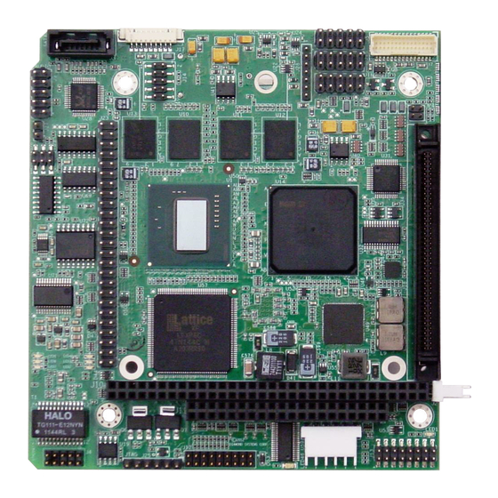
5. BOARD DESCRIPTION The figure below shows the Athena III SBC layout with connector and jumper block locations labeled. On the following page is a figure showing the key dimensions on the Athena III PCB in millimeters. J5 J15 J16 www.diamondsystems.com... - Page 17 Athena III User Manual Rev A.03 Page...
-
Page 18: Connector Summary
Connector Summary The following table lists the connectors on the Athena III SBC. Connector Description External Battery SATA Ethernet LVDS LCD LCD Backlight Power (on bottom of SBC) Audio I/O PC/104, ISA bus A,B PC/104, ISA bus C,D USB flashdisk... -
Page 19: Led Summary
LED Summary The following table lists the LEDs found on the Athena III SBC. LED Number Description Color LED46 DAQ/FPGA loaded successfully Blue LED1 SATA activity Green LED2 Ethernet activity Green LED3 Ethernet Link 100Mbps Green LED4 Ethernet Link 1000Mbps... -
Page 20: Connectors
6. CONNECTORS This section describes the on-board Athena III connectors. Note: All cables mentioned in this chapter are included in Diamond Systems’ cable kit C-ATHE-KIT. Some cables are also available individually. External Battery (J2) Connector J2 is used to connect an external battery for maintaining the Real-Time Clock and the CMOS settings (BIOS settings for various system configurations). -
Page 21: Ethernet (J4)
Ethernet (J4) Athena III provides one Gigabit Ethernet port. The I/O connector pinout is designed so that the left column matches the 10/100 Ethernet pinout on Athena II for backward compatibility with existing Athena II mating cables and applications. For Gigabit operation all 10 pins are used. -
Page 22: Lcd Panel, Lvds Interface (J7)
(only powered up when LCD display is active) Ground Power Ground, 0V Connector on board: JST model number BM30B-SRDS-G-TF or equivalent Mating cable connector: JST model number SHDR-30V-S-B or equivalent Terminals: JST model number SSH-003GA-P0.2 or equivalent www.diamondsystems.com Athena III User Manual Rev A.03 Page... -
Page 23: Lcd Backlight (J8)
Connector J9 provides the audio signals. Line Out Left Line Out Right Ground Line In left Lin In Right Ground MIC In Ground Connector type: Standard 0.1” dual row straight pin headers with gold flash plating www.diamondsystems.com Athena III User Manual Rev A.03 Page... -
Page 24: Pc/104 Isa Bus (J10, J11)
DACK3- SD11 DACK7- SA15 DRQ3 SD12 DRQ7 SA14 DACK1- SD13 SA13 DRQ1 SD14 MASTER- SA12 REFRESH- SD15 Ground SA11 SYSCLK Ground SA10 IRQ7 IRQ6 IRQ5 IRQ4 IRQ3 DACK2- BALE Ground Ground Ground www.diamondsystems.com Athena III User Manual Rev A.03 Page... -
Page 25: Usb Flashdisk (J14)
Data + Data - Ground Connectors J15 and J16 mate with Diamond Systems cable number 698012, which provides two standard USB type A jacks in a panel-mount housing. Connector type: Standard 0.1” dual row straight pin headers with gold flash plating www.diamondsystems.com... -
Page 26: Main I/O (J18)
For RS-422 or RS-485, the following pinouts apply: 1/10/19/28 1/10/19/28 2/11/20/29 2/11/20/29 3/12/21/30 TXD+ 3/12/21/30 4/13/22/31 TXD- 4/13/22/31 TXD/RXD- RS-422 5/14/23/32 Ground RS-485 5/14/23/32 TXD/RXD+ 6/15/24/33 RXD- 6/15/24/33 7/16/25/34 RXD+ 7/16/25/34 8/17/26/35 8/17/26/35 9/18/27/36 Ground 9/18/27/36 Ground www.diamondsystems.com Athena III User Manual Rev A.03 Page... - Page 27 Utilities B RI4 35 35 Reset- GND 36 36 Power Utilities A +5V Out 37 37 NC Speaker Out 38 38 NC SATA Drive LED 39 39 NC Power LED 40 40 NC www.diamondsystems.com Athena III User Manual Rev A.03 Page...
- Page 28 CPU to turn on, and a contact of 4 seconds or longer will generate a power shutdown. Connector J18 mates with Diamond Systems cable number C-PRZ-01, which consists of a dual-ribbon-cable assembly with industry-standard connectors at the user end. The SBC mating connector includes integral latches for enhanced reliability.
-
Page 29: Input Power (J21)
Multiple +5V and Ground pins are provided for extra current carrying capacity if needed. Each pin is rated at 3A max (15W). For the Athena III SBC and panel I/O board 3A is sufficient, so +5V and Ground require only a single wire each. In this case the first 4 pins may be connected to a standard 4-pin miniature PC power connector if desired. -
Page 30: Data Acquisition I/O (J23)
Data Acquisition I/O (J23) J23 Data Acquisition I/O Connector Athena III includes a 50-pin header, J23, for all data acquisition I/O with the pin out below. DIO A0 DIO A1 DIO A2 DIO A3 DIO A4 DIO A5 DIO A6... -
Page 31: Jumper Configuration
Analog ground; used for analog circuitry only Vout pin is for analog outputs, Vin pin is for analog inputs Diamond Systems cable number C-50-18 provides a standard 50-pin connector at each end and mates with this header. Connector type: Standard .1” single row straight pin header with gold flash plating 7. -
Page 32: Lcd Panel Voltage Select (Jp5)
Jumper block JP6 is used to configure IRQ levels. JP6 Jumper Block with Default Settings Pin Number Function 7, 9 IRQ 15; selectable for COM4 14,16 IRQ 5; selectable for A/D IRQ 17,18 IRQ 6; selectable for COM3 www.diamondsystems.com Athena III User Manual Rev A.03 Page... - Page 33 It is possible to set up all three circuits to share either IRQ4 or IRQ5. However, only one device can use the shared IRQ at a time; the ability for all three devices to run simultaneously is not supported. Configure the IRQ options as shown in the following jumper settings. IRQ Configuration Options www.diamondsystems.com Athena III User Manual Rev A.03 Page...
-
Page 34: Rs-232/422/485 Termination Select (Jp7)
Differential inputs are frequently used either when the grounds of the input device and the measurement device (Athena III) are at different voltages, or when a low-level signal is being measured that has its own ground wire. A differential input also has higher noise immunity than a single-ended input because most noise affects both (+) and (–) input wires equally, so the noise is canceled out in the measurement. -
Page 35: Unipolar/Bipolar Input Settings
Athena III can be configured for either 16 single-ended inputs, or eight differential inputs, as shown below. A/D Single-ended/Differential Selection The default setting is single-ended mode. -
Page 36: System Operation
A serial port on another PC can be connected to the serial port on Athena III with a null modem cable, and a terminal emulation program, such as HyperTerminal, can be used to establish the connection. The terminal program must be capable of transmitting special characters including F2 (some programs or configurations trap special characters). -
Page 37: Flash Memory
4. Exit the BIOS and save your settings. Flash Memory Athena III contains a 2048KB, 16-bit wide flash memory chip for storage of BIOS and other system configuration data. Backup Battery Athena III contains an integrated RTC/CMOS RAM backup battery. This battery has a capacity of 120mAH and will last over three years in power-off state. -
Page 38: Bios
9. BIOS Athena III uses a BIOS from American Megatrends modified to support the custom features of the Athena III SBC. BIOS Settings To change the following BIOS settings, press F2 during system startup power on self-test (POST). 9.1.1 Serial Ports The address and interrupt settings for serial ports COM1 and COM2 may be modified. -
Page 39: Bios Console Redirection Settings
Console Connection: Direct (default) or Modem. Console Type: PC ANSI (default), VT100, VT100 (8-bit), PC-ANSI (7-bit), VT100+, or VT-UTF8. Flow Control: CTS/RTS (default), XON-XOFF, None. Number of video Pages to support: 1(default) to 8. www.diamondsystems.com Athena III User Manual Rev A.03 Page... -
Page 40: System I/O
10.2 Serial Ports Athena III contains four serial ports. Each port is capable of transmitting at speeds up to 115.2Kbaud. Ports COM1 and COM2 are built into the standard chipset, which are standard 16550 UARTs with 16-byte FIFOs. Ports COM3 and COM4 are derived from an Exar 16C2850 dual UART chip and include 128-byte FIFOs. These ports may be operated at speeds to 1.5Mbaud with installation of high-speed drivers, as a custom option. -
Page 41: Usb Ports
3. Insert the DOS installation floppy disk into the USB floppy drive and start/restart the system. 4. Install any drivers needed. Note: For DOS Ethernet, set Operating System to other in the BIOS. Note: DOS Sound emulation is currently not functional. www.diamondsystems.com Athena III User Manual Rev A.03 Page... -
Page 42: Data Acquisition Circuit
12. DATA ACQUISITION CIRCUIT Athena III contains a data acquisition subsystem consisting of A/D, D/A, digital I/O, and counter/timer features. This subsystem is equivalent to a complete add-on data acquisition module. The A/D section includes a 16-bit A/D converter, 16 input channels, and a 2048-sample FIFO. Input ranges are programmable, and the maximum sampling rate is 200KHz. -
Page 43: Data Acquisition Circuitry I/O Map
Data Acquisition Circuitry I/O Map 12.1.1 Overview The data acquisition circuitry on Athena III occupies 16 bytes in I/O memory space. The default address range is 280h (base address) to 28Fh. The data acquisition FPGA can be enabled/disabled in the BIOS under the Advanced menu. Scroll down to the “FPGA Mode”... -
Page 44: Register Map Bit Summary
Base + CtrD7 CtrD6 CtrD5 CtrD4 CtrD3 CtrD2 CtrD1 CtrD0 CtrD15 CtrD14 CtrD13 CtrD12 CtrD11 CtrD10 CtrD9 CtrD8 CtrD23 CtrD22 CtrD21 CtrD20 CtrD19 CtrD18 CtrD17 CtrD16 CTRNO LATCH GTDIS GTEN CTDIS CTEN LOAD www.diamondsystems.com Athena III User Manual Rev A.03 Page... - Page 45 Page 2 Write Register Summary Base + EXFIFO DACPOLE DACPOL ADPOL ADPOLEN ADSD ADSDEN SCANINT DAQ_LED Page 2 Read Register Summary Base + EXFIFO DACPOLEN DACPOL ADPOL ADPOLEN ADSD ADSDEN SCANINT -- 0xA2 -- www.diamondsystems.com Athena III User Manual Rev A.03 Page...
-
Page 46: Main Registers
The user’s interrupt routine must write to the appropriate bit prior to exiting in order to enable future interrupts. Otherwise the interrupt line will stay high indefinitely and no additional interrupt requests will be generated by the board. www.diamondsystems.com Athena III User Manual Rev A.03 Page... - Page 47 A/D data bits 15 – 8; AD15 is the MSB; A/D data is an unsigned 16-bit value. AD15 - 8 See Base + 0 Read on the previous page for information on A/D values and formulas. www.diamondsystems.com Athena III User Manual Rev A.03 Page...
- Page 48 LOW and HIGH. For example, if LOW = 0 and HIGH = 3, the A/D channels will progress through the following sequence: 0, 1, 2, 3, 0, 1, 2, 3, 0, 1, …. Reading from this register returns the value previously written to it. www.diamondsystems.com Athena III User Manual Rev A.03 Page...
- Page 49 Only one ADWAIT period must be observed between the last triggering condition (write to Base + 2 or Base + 3) and the start of an A/D conversion. The following table lists the possible analog input ranges: ADG1 ADG0 Gain Unipolar Range Bipolar Range 0-10V ±10V 0-5V ±5V 0-2.5V ±2.5V 0-1.25V ±1.25V www.diamondsystems.com Athena III User Manual Rev A.03 Page...
- Page 50 SCANEN Scan mode readback (see Base + 3 Write above). ADG1-0 A/D gain setting readback (see Base + 3 Write above). www.diamondsystems.com Athena III User Manual Rev A.03 Page...
- Page 51 The user’s interrupt routine must monitor the status bits to know which circuit has requested service. After processing the data but before exiting, the interrupt routine must then clear the appropriate interrupt request bit using the register at Base + 0. www.diamondsystems.com Athena III User Manual Rev A.03 Page...
- Page 52 When EXFIFO = 1 (Enhanced Mode, See Register Description for Page 2 Base+12) Current FIFO Depth LSB. This value indicates the lower 8 bits of the number of A/D values currently stored in the FIFO. www.diamondsystems.com Athena III User Manual Rev A.03 Page...
- Page 53 FIFO Full Bit. The next conversion will result in an overflow. FIFO Half Full Bit. FIFO is at least half full containing at least 1k words of A/D data. FIFO Empty. FIFO is empty. www.diamondsystems.com Athena III User Manual Rev A.03 Page...
- Page 54 Read / Write Digital I/O Port B Bit No. Name Reset These registers are used for digital I/O on PortB. The direction of each register is controlled by the DIO control register at Base+11. www.diamondsystems.com Athena III User Manual Rev A.03 Page...
- Page 55 Instead, a read of the register at Page 2, Base+15 will cause the update of the D/A converter. Base + 11 Read Digital I/O and DA Control Register Readback Bit No. Name DASIM DIRA DIRCH DIRB DIRCL Reset Read-back of Base+11. www.diamondsystems.com Athena III User Manual Rev A.03 Page...
-
Page 56: Counter / Timer Control
1, this register is ignored. When reading from this register, the MSB value of the most recent Latch command for counter 0 will be returned. The value returned is NOT the value written to this register. www.diamondsystems.com Athena III User Manual Rev A.03 Page... - Page 57 FPGA Revision Code Bit No. Name REV7 REV6 REV5 REV4 REV3 REV2 REV1 REV0 Reset REV7-0 Revision code, read as a 2-digit hex value. The first rev of this FPGA should be 0x48. www.diamondsystems.com Athena III User Manual Rev A.03 Page...
-
Page 58: Register Definitions
TDACWR TrimDAC Write. Writing 1 to this bit will initiate a transfer to the TrimDAC addressed by the register at page 1, base+13. (used in the autocalibration process). If both EE_EN and TDACWR are set to ‘1’ then TDACWR is ignored. www.diamondsystems.com Athena III User Manual Rev A.03 Page... -
Page 59: Register Definitions
11-bit value. ADC Expanded FIFO: Base+12 (Write) Bit: Name: ADCEXF ADCEXF ADC expanded FIFO mode flag. 0 = Not in expanded FIFO mode. 1 = In expanded FIFO mode. www.diamondsystems.com Athena III User Manual Rev A.03 Page... - Page 60 Enable ADSD. When this bit is set the ADSD setting is output to the DAC circuit. Page 2 Select Read Back Check: Base+15 (Read) Bit: Name: PG2ID PGID Register page 2 ID. This register always contains the value 0xA2. www.diamondsystems.com Athena III User Manual Rev A.03 Page...
-
Page 61: Analog-To-Digital Input Ranges And Resolution
Overview Athena III uses a 16-bit A/D converter. The full range of numerical values for a 16-bit number is 0 - 65535. However, the A/D converter uses two’s complement notation, so the A/D value is interpreted as a signed integer, ranging from –32768 to +32767. -
Page 62: Performing An A/D Conversion
A/D if AINTE = 0 (interrupts are disabled). When AINTE = 1, the A/D can only be triggered by the on- board counter/timer or an external signal. This protects against accidental triggering by software during a long- running interrupt-based acquisition process. outp(base,0x80); www.diamondsystems.com Athena III User Manual Rev A.03 Page... -
Page 63: Wait For The Conversion To Finish
FIFO. The FIFO depth register increments by the scan size. When STS goes low, the program should read out the data for all channels. www.diamondsystems.com Athena III User Manual Rev A.03 Page... -
Page 64: Convert The Numerical Data To A Meaningful Value
A/D Code Input Voltage Symbolic Formula Input Voltage for 5V Range -32768 -5.0000V -32767 + 1 LSB -4.9998V -1 LSB -0.00015V 0.0000V +1 LSB 0.00015V 32767 - 1 LSB 4.9998V www.diamondsystems.com Athena III User Manual Rev A.03 Page... -
Page 65: Conversion Formula For Unipolar Input Ranges
Input Voltage for 5V Range -32768 0.0000V -32767 1 LSB (V / 65536) 0.000076V / 2 - 1 LSB 2.4999V 2.5000V / 2 + 1 LSB 2.5001V 32767 - 1 LSB 4.9999V www.diamondsystems.com Athena III User Manual Rev A.03 Page... -
Page 66: A/D Scan, Interrupt And Fifo Operation
The table on the next page describes the board’s behavior for each of the 4 possible cases of AINTE and SCANEN. The given interrupt software behavior describes the operation of the Diamond Systems Universal Driver software. If you write your own software or interrupt routine you should conform to the described behavior for optimum results. - Page 67 STS stays high during the entire scan (multiple A/D conversions). A/D interrupt occurs when the FIFO reaches its programmed threshold. The interrupt routine reads the number of samples equal to the FIFO threshold (Base+5, bits 0-5). www.diamondsystems.com Athena III User Manual Rev A.03 Page...
-
Page 68: Digital-To-Analog Output Ranges And Resolution
16.1 Description Athena III uses a 4-channel 12-bit D/A converter (DAC) to provide four analog outputs. A 12-bit DAC can generate output voltages with the precision of a 12-bit binary number. The maximum value of a 12-bit binary number is 2 - 1, or 4095, so the full range of numerical values that the DACs support is 0 - 4095. -
Page 69: D/A Conversion Formulas And Tables
Output Voltage for 0-10V Range 0.0000V 1 LSB (V / 4096) 0.0024V 2047 / 2 - 1 LSB 4.9976V 2048 5.0000V 2049 / 2 + 1 LSB 5.0024V 4095 - 1 LSB 9.9976V www.diamondsystems.com Athena III User Manual Rev A.03 Page... -
Page 70: D/A Conversion Formulas For Bipolar Output Ranges
(VREF = Reference voltage). D/A Code Output Voltage Symbolic Formula Output Voltage for 10V Range -10.0000V + 1 LSB -9.9951V 2047 -1 LSB -0.0049V 2048 0.0000V 2049 +1 LSB 0.0049V 4095 - 1 LSB 9.9951V www.diamondsystems.com Athena III User Manual Rev A.03 Page... -
Page 71: Generating An Analog Output
The status bit DACBUSY (Base+3, bit 4) indicates if the D/A is busy updating (1) or idle (0). After writing to the D/A, monitor DACBUSY until it is zero before continuing with the next D/A operation. www.diamondsystems.com Athena III User Manual Rev A.03 Page... -
Page 72: Analog Circuit Calibration
18. ANALOG CIRCUIT CALIBRATION The Athena III data acquisition circuit contains an advanced autocalibration circuit that can maintain the accuracy of both A/D and D/A circuits to within the specified tolerances regardless of time and temperature. Autocalibration is supported in the Diamond Systems Universal Driver software included with the board. -
Page 73: Digital I/O Operation
19. DIGITAL I/O OPERATION Athena III contains 24 digital I/O lines organized as three 8-bit I/O ports: Port A, Port B, and Port C. The direction of each port is programmable, and port C is further divided into two 4-bit halves, each with independent direction. -
Page 74: Counter/Timer Operation
20. COUNTER/TIMER OPERATION Athena III contains two counter/timers that provide various timing functions on the board for A/D timing and user functions. These counters are controlled with registers in the on-board data acquisition controller FPGA. Counter 0 – A/D Sample Control 20.1... -
Page 75: Command Sequences
20.3 Command Sequences Diamond Systems provides driver software to control the counter/timers on Athena III. The information in this section is intended as a guide for programmers writing their own code, instead of using the driver, and to give a better understanding of the counter/timer operation. -
Page 76: Disabling The Counter Gate Command
The value is returned in 3 bytes, low, middle, and high (2 bytes for counter 1). Counter 0: Counter 1: low=inp(base+12); low=inp(base+12); middle=inp(base+13); high=inp(base+13); high=inp(base+14); 23. Clear the counter. Counter 0: Counter 1: outp(base+15,0x01); outp(base+15,0x81); www.diamondsystems.com Athena III User Manual Rev A.03 Page... -
Page 77: Usb Flashdisk Module
21. USB FLASHDISK MODULE Athena III is designed to accommodate an optional solid-state USB flashdisk module. This module contains 1GB to 8GB of solid-state non-volatile memory that operates like an USB drive without requiring additional driver software support. Model Capacity... -
Page 78: Bios Option Listing
Save changes and exit BIOS setup mode At any time, select Save & Exit to exit BIOS setup mode. Use the up/down arrow keys, followed by carriage return, to apply one of the exit actions. www.diamondsystems.com Athena III User Manual Rev A.03 Page... -
Page 79: Bios Screen Descriptions
This section describes the screen displays for each BIOS setup area. The data in the fields are examples only and may be different depending on future product releases from Diamond Systems or the user’s configuration. Sub-menus are prefixed with a . - Page 80 Bootup NumLock State [On] CSM16 Module Version 07.65 GateA20 Active [Upon Request] Option ROM Messages [Force BIOS] Interrupt 19 Capture [Disabled] Boot Option Priorities Boot Option #1 [Disabled] Security Administrator Password User Password www.diamondsystems.com Athena III User Manual Rev A.03 Page...
- Page 81 Discard Changes and Exit Save Changes and Reset Discard Changes and Reset Save Options Save Changes Discard Changes Restore Defaults Save as User Defaults Restore as User Defaults Boot Override Built-in EFI Shell www.diamondsystems.com Athena III User Manual Rev A.03 Page...
-
Page 82: Specifications
A/D and D/A Calibration: Automatic using on-board microcontroller and temperature sensor Analog Outputs: 4, 12-bit resolution Output ranges: ±5V, ±10V, 0-5V, 0-10V Output current: ±5mA max per channel Settling time: 7µS max to 0.01% Relative accuracy: ±1 LSB Nonlinearity: ±1 LSB, monotonic www.diamondsystems.com Athena III User Manual Rev A.03 Page... -
Page 83: Power Supply
Power Supply Input Voltage: +5VDC ±5% Power consumption: 9.4W 23.4 General Shock: IEC68-2-27 compatible Vibration: MIL-STD-810E 514.4 compatible Dimensions: 4.18 x 4.48 in. (106 x 114mm) Weight: 8.8oz.(249g) with heat sink RoHS: Compliant www.diamondsystems.com Athena III User Manual Rev A.03 Page...
Need help?
Do you have a question about the Athena III and is the answer not in the manual?
Questions and answers