Table of Contents
Advertisement
Quick Links
Advertisement
Table of Contents

Related Manuals for Diamond Systems ZETA


Summary of Contents for Diamond Systems ZETA
- Page 1 ZETA COM-based SBC based on Type 10 nano COM Modules Revision Date Comment 9/6/2018 Initial release from v0.7 Copyright 2018 FOR TECHNICAL SUPPORT Diamond Systems Corporation PLEASE CONTACT: www.diamondsystems.com support@diamondsystems.com www.diamondsystems.com Zeta User Manual Rev 1.0...
-
Page 2: Table Of Contents
Mechanical, Electrical, Environmental ......................8 Operating System Support ..........................8 Customization Options ................... Error! Bookmark not defined. Feature support limitations of Zeta Board with ARBOR and DFI COM modules: ..Error! Bookmark not defined. Functional Overview ..................Error! Bookmark not defined. Functional Block Diagram ................Error! Bookmark not defined. - Page 3 9.6.1 Connector Table ..........................34 9.6.2 I/O Cables ....................Error! Bookmark not defined. Mechanical Board Drawing of Zeta daughter board .................. 34 Connector and jumper location ......................... 35 10 Mass storage ............................36 10.1 List of options ............................. 36 10.2 Installation and configuration ........................36 10.3 Photos of installed modules ................
- Page 4 Overview ............................50 11.7.2 Interrupt Sources ..........................50 12 “D” Model DAQ Architecture overview....................51 12.1 Block Diagram ............................. 52 12.2 Digital IO specification ..........................52 12.3 Configuration and Programming ........................ 52 www.diamondsystems.com Zeta User Manual Rev 1.0 Page 4...
-
Page 5: Important Safe Handling Information
The list here describes common causes of failure found on boards returned to Diamond Systems for repair. This information is provided as a source of advice to help you prevent damaging your Diamond (or any vendor’s) embedded computer boards. -
Page 6: Introduction
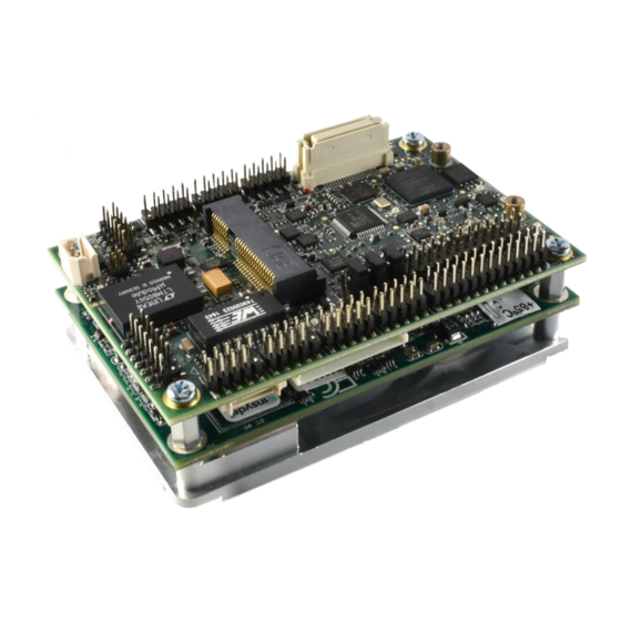
55 x 84 mm / 2.2 x 3.3 inches. The use of a miniature COM plus a same-size baseboard enables Zeta to deliver an impressive array of features and performance in a very small size, achieving as much as a 60% reduction in area compared to other form factors such as PC/104. -
Page 7: Features
Core I/O features common to all models of Zeta include the following: Feature Value Serial ports 4x RS-232/422/485 USB2.0 USB3.0 Input voltage 6-36VDC Gigabit Ethernet ports VGA display 1 single channel LVDS display Micro-SD socket Mini PCIe / mSATA socket Expansion connector PCIe x 1 –... -
Page 8: Mechanical, Electrical, Environmental
-40°C to +85°C at the external surface of the heat spreader Operating System Support Linux Ubuntu 16.04 LTS (all models) Windows 7 (E3815 models only) Windows 10 IoT (E3940 / N4200 models only) www.diamondsystems.com Zeta User Manual Rev 1.0 Page 8... -
Page 9: Functional Block Diagram
3 Block Diagram Figure 1: Functional Block Diagram www.diamondsystems.com Zeta User Manual Rev 1.0 Page 9... -
Page 10: Feature Description
4.1 Power Supply Zeta base board can be powered either from any DC power supply with an output voltage range of +6V to +36V. This range makes Zeta compatible with standard power supply voltages of 12V, 24V, and 28V. In addition, Zeta can operate in a vehicle environment due to its ability to run on 6VDC. -
Page 11: Msata/Pcie Mini-Card Socket
4.12 Data Acquisition Zeta base board provides a data acquisition sub circuit containing analog input, analog output, and digital I/O features. This circuit is controlled by an FPGA attached to the processor via the LPC bus. A pin header on the board provides access to JTAG signals for reprogramming the FPGA on the board and in the field. - Page 12 The form factor of the board is COM Express Nano Type 10 with dimensions 55mm x 84mm. Figure 2: Mechanical outline, top view Figure 3: Mechanical outline, Side view www.diamondsystems.com Zeta User Manual Rev 1.0 Page 12...
-
Page 13: Connector And Jumper Locations
6 I/O Connector and Jumper Locations Figure 4 : Zeta board connectors and jumpers - Top side www.diamondsystems.com Zeta User Manual Rev 1.0 Page 13... - Page 14 Figure 5 : Zeta board connectors - Bottom side www.diamondsystems.com Zeta User Manual Rev 1.0 Page 14...
-
Page 15: Getting Started
Systems’ software and hardware development kits include a mSATA with pre-loaded OS. Zeta base board can be booted from micro SD card for linux OS. Zeta base board can be booted from an external hard drive connected mini card to SATA adapter board. -
Page 16: Installing Os And Booting
The following steps describe how to install an operating system from a mSATA using Arbor module. Follow the below steps to install a 32-bit Windows 7 legacy operating system on a mSATA. Connect a USB pen drive to a USB port of (J1 or J4) of Zeta base board having 32-bit Windows 7 installation image. ... -
Page 17: Connector Pinout And Pin Description
Each connector pin can support up to 2A. The number of connections can be determined by the total power consumption of the Zeta board plus all attached I/O (daughterboard, mSATA and mini PCIe modules, and USB devices) divided by the input voltage, divided by 2A. -
Page 18: Rs485 Mode
One USB 3.0 port is provided on connector J4. The pinout for the connector is shown below: USB Pwr+ USB_SSRX0- USB Pwr+ USB_SSRX0+ GND (USB Pwr-) USB_SSTX0- GND (USB Pwr-) USB_SSTX0+ Ethernet (J11 and J12) www.diamondsystems.com Zeta User Manual Rev 1.0 Page 18... -
Page 19: Msata / Mpcie (J8)
SMB Data PCIe 0 TX+ SATA 0 TX+ USB2_N USB2_P +3.3V +3.3V +3.3V +3.3V WWAN LED- Ground Ground WLAN LED- WPAN LED- +1.5V Pull-up to +3.3V Pull-up to +3.3V +3.3V Micro SD (J17) www.diamondsystems.com Zeta User Manual Rev 1.0 Page 19... -
Page 20: Vga (J3)
The single-channel LVDS interface is provided on connector J18. The pinout is shown below: VCC_5V_LVDS_CON V_3P3_LVDS_CON LVDS_A_CH_CLK_P LVDS_A_CH_CLK_N LVDS_A_CH_0_P LVDS_A_CH_0_N LVDS_A_CH_1_P LVDS_A_CH_1_N LVDS_A_CH_2_P LVDS_A_CH_2_N LVDS_A_CH_3_P LVDS_A_CH_3_N LVDS_DDC_CLK LVDS_DDC_DAT 8.11 LCD Backlight (J19) www.diamondsystems.com Zeta User Manual Rev 1.0 Page 20... -
Page 21: Analog I/O (J10)
Vin 6 / 6+ Vin 14 / 6- Vin 7 / 7+ Vin 15 / 7- DIO D0 DIO D1 DIO D2 Dground Note: This connector will not be used in D-model. www.diamondsystems.com Zeta User Manual Rev 1.0 Page 21... -
Page 22: Digital I/O (J15)
8.13 Digital I/O (J15) The pinout for the Zeta A model is shown below. DIO A0 DIO A1 DIO A2 DIO A3 DIO A4 DIO A5 DIO A6 DIO A7 DIO B0 DIO B1 DIO B2 DIO B3 DIO B4... -
Page 23: Expansion Connector (J5)
PCIe_Exp2_T+ (NC) PCIe_Exp1_T+ PCIe_Exp2_T‐(NC) PCIe_Exp1_T‐ PCIe_Exp2_R+(NC) PCIe_Exp1_R+ PCIe_Exp2_R‐(NC) PCIe_Exp1_R‐ PCIe_Exp2_C+(NC) PCIe_Exp1_C+ PCIe_Exp2_C‐(NC) PCIe_Exp1_C‐ +3.3V SATA‐T+ PCIe_Exp1_clkreq‐(NC) SATA‐T‐ PCIe_Exp2_clkreq‐(NC) +3.3V USB2_D4_P SATA‐R+ USB2_D4_N SATA‐R‐ +3.3V Host Reset‐ AC_SDIN0 I2C_Data AC_BITCLK I2C_Clk AC_SDOUT AC_SYNC AC_RST# www.diamondsystems.com Zeta User Manual Rev 1.0 Page 23... - Page 24 AC_SDOUT HD Audio Link AC_RST# AC_SYNC I2C_Data I2C interface I2C_Clk USB2_D4_P USB2.0 Interface USB2_D4_N Host Reset‐ Reset from Processor 5V supply from Carrier board +3.3V 3.3V supply from Carrier board Digital ground www.diamondsystems.com Zeta User Manual Rev 1.0 Page 24...
-
Page 25: List Of Connectors
PCIe Minicard 52-pin Minicard, full size / mSATA Expansion 2x20 .635mm / .025” pitch SMD Molex 53627-0474 Connector SD Card 10 (8 + 2) Position Card Connector Table 1: Zeta board connector details www.diamondsystems.com Zeta User Manual Rev 1.0 Page 25... -
Page 26: O Cables
10 I/O Cables The Zeta cable kit includes cables for all I/O features on Zeta except LCD. Details are provided below. Individual cables are available as a special order item. Minimum order quantities and lead times may apply. An LCD / backlight cable kit is available for specific displays used in our manufacturing environment. -
Page 27: Jumper Descriptions
Figure 7: Zeta default jumper location Jumper Position Description LVDS PWM =3.3V LVDS PWM =5V VIO_DIO = 3.3V VIO_DIO = 5.0V 9-10 DIO Pulled up 11-12 DIO Pulled down Table 3: Zeta board Jumper JP1 details www.diamondsystems.com Zeta User Manual Rev 1.0 Page 27... -
Page 28: Zeta Daughter Board
12 Zeta daughter board 12.1 Description Zeta includes an expansion connector which supports the installation of a daughterboard with additional I/O and expansion features: • Full/half-size MiniCard socket with PCIe x1 and USB2.0 connectivity • M.2 M-keying SSD connector for 2242 size PCIe flash modules •... -
Page 29: Feature Description
*Second PCIe port will be unused in the daughter board. 12.4.2 Power Supply Zeta daughter board is powered from 5V and 3.3V on the expansion connector. The 1.5V required for the PCIe Mini card socket is generated with a 3.3V to 1.5V LDO. 12.4.3 PCIe PCIe lane 1 from the expansion connector is connected to PCIe Minicard socket;... -
Page 30: Jumper Configuration
Refer the below jumper settings to change the configuration for DIO signals. Jumper Position Configuration VIO_DIO = 3.3V VIO_DIO = 5V DIO Pulled up DIO Pulled down Table 5: Zeta daughter board jumper details www.diamondsystems.com Zeta User Manual Rev 1.0 Page 30... -
Page 31: Connector Pinout And Pin Description
Mini card socket pin outs are provided below. +3.3V +1.5V Clkreq- PCIe 1 Clk- PCIe 1 Clk+ Disable- PCIe Reset- PCIe 1 RX- +3.3V PCIe 1 RX+ +1.5V SMB Clk PCIe 1 TX- SMB Data PCIe 1 TX+ USB2_N www.diamondsystems.com Zeta User Manual Rev 1.0 Page 31... -
Page 32: Sata Ssd Socket
Note: All TX/RX signals are with respect to the host. TX on the socket drives RX on the installed module, and RX on the socket is driven by TX on the installed module. One mounting standoffs at the far end of the module installation site are not connected to ground. www.diamondsystems.com Zeta User Manual Rev 1.0 Page 32... -
Page 33: Audio
DIO B2 DIO B3 DIO B4 DIO B5 DIO B6 DIO B7 Dground Dground 12.5.6 USB-I2C header USB I2C header pinouts are provided below. USB2+ I2C CLK USB2- I2C DATA USB_5V 3P3/5V0 www.diamondsystems.com Zeta User Manual Rev 1.0 Page 33... -
Page 34: Connector And Cable Information
Table 6: Zeta daughter board connectors 12.7 Mechanical Board Drawing of Zeta daughter board The form factor of Zeta daughter board is COM express Nano Type 10 with dimensions 55 x 84 mm. Figure 9: Mechanical outline top view www.diamondsystems.com Zeta User Manual Rev 1.0... -
Page 35: Connector And Jumper Location
12.8 Connector and jumper location Figure 10: Zeta daughter board connectors and jumpers – Top side Figure 11: Zeta daughter board connectors– Bottom side www.diamondsystems.com Zeta User Manual Rev 1.0 Page 35... -
Page 36: Mass Storage
13.2 Installation and configuration To install any of the above SATA flash disk devices, locate the desired mSATA (J8) port Zeta base board or M.2 socket(J1) on Zeta daughter board ports. Plug the flash disk module into the appropriate port. -
Page 37: 11 "A" Model Daq Architecture Overview
14 “A” Model Data Acquisition Circuit Zeta is available in two configurations. Both configurations are available with any processor option. • The “D” model provides 16 GPIO lines with 3.3V/5V logic compatibility and jumper-selectable pull-up/down resistors. • The “A” model features a comprehensive data acquisition circuit providing 16 SE / 8 DI analog inputs with +/-10V, +/-5V, 0-10V, and 0-5V input ranges, 100KHz max sample rate with2048- sample FIFO, 4 analog outputs with 0-5V and 0-2.5V ranges, 27 GPIO instead of 16, 4 32-bit... -
Page 38: Block Diagram
A/D Circuit Overview Zeta base board “A” models include an analog input circuit based on the LTC1859 16-bit A/D converter, or ADC. The LTC1859 is capable of operating at up to 100,000 samples per second in total, either on a single channel or on any number of channels. -
Page 39: A/D Fifo And High Speed Sampling
The Diamond Systems Universal Driver software provides full support for high speed A/D sampling with FIFO and interrupt support. Please refer to that user manual for operating details. When using Universal Driver software, the interrupt rate is equal to the total A/D sample rate divided by the programmed FIFO threshold, because each time the interrupt service routine runs, it will read out the number of samples equal to the threshold value. -
Page 40: A/D Operation
Significant Bit). The resolution is always 16 bits, but the value of 1 LSB will vary with the input range. Polarity Input Range Resolution (1LSB) Bipolar ±10V 305µV Bipolar ±5V 153µV Unipolar 0 - 10V 153µV Unipolar 0 - 5V 76µV www.diamondsystems.com Zeta User Manual Rev 1.0 Page 40... -
Page 41: Input Range Selection
5V or 10V. Example: For unipolar input range 0-5V, full-scale input voltage = 5V. For an A/D value of 17761: Input voltage = 17761 / 65536 * 5V = 1.355V www.diamondsystems.com Zeta User Manual Rev 1.0 Page 41... -
Page 42: Measurement Accuracy And Calibration
A/D in the middle. The higher the output impedance of the input signal, the greater the error will be. Conversely, the higher the input impedance of the A/D circuit, the lower the error will be. Zeta base board uses high impedance, ultra-low-offset buffer op amps to boost the input impedance to well over 10 GigOhms (the input impedance is calculated based on the specified input current of 75pA). -
Page 43: Digital-To-Analog Circuit
14.3.1 Overview The Zeta base board data acquisition circuit uses a 16-bit D/A converter. This means that all output voltages are defined by a 16-bit binary number, or D/A code, ranging from 0 to 65535 (2 -1), or binary 0000 0000 0000 0000 to 1111 1111 1111 1111. -
Page 44: D/A Conversion Formula
To minimize the size and cost of the D/A circuit while still providing reasonable performance, the D/A circuit on Zeta base board does not provide calibration features to eliminate these errors. Instead the circuit was designed to minimize the inherent offset, gain, and drift characteristics. The specifications at the end of this manual indicate the worst-case offset, gain, and temperature drift errors in the circuit. -
Page 45: Digital I/O Features
On “A” models, an edge detection circuit is available on port B. The edge detection circuit can be used to notify the processor when a particular event occurs, such as a door opening, a switch being pressed, or a light curtain being penetrated. www.diamondsystems.com Zeta User Manual Rev 1.0 Page 45... -
Page 46: Support For Special Functions
The edge detection circuit on Zeta contains an enable register, a polarity register, and a status register. The programmer can specify which bits will be active with the enable register and which transition to detect on each bit (0 to 1 or 1 to 0) with the polarity register. The status register indicates which bits have seen the specified change since the last time it was read. -
Page 47: Counter/Timer Features
14.5.1 Overview Zeta “A” models include 8 32-bit counter/timers with a wide array of features and programmability. Both up and down counting are supported, and the clock for each counter can be selected from an internal 50MHz or 1MHz clock or an external digital signal. In down counting mode, an optional programmable-width output pulse may be enabled each time the counter reaches zero. -
Page 48: Counter Advanced Features
The DAQ circuit uses counter/timers to control the A/D sample rate for high speed sampling as well as the D/A waveform generator data rate. These operations are managed by the Universal Driver software. Refer to the Universal Driver user manual for details on these advanced features. www.diamondsystems.com Zeta User Manual Rev 1.0 Page 48... -
Page 49: Pulse Width Modulator Features
14.6.1 Overview Zeta “A” models include 4 24-bit pulse width modulator circuits (PWMs). These circuits can be programmed to produce an output square wave up to 25MHz with a duty cycle anywhere from 0% to 100% (these limits are of course DC signals). -
Page 50: Interrupt Operation
The primary host interface for the Zeta base board “A” model data acquisition circuit is the SPI bus. However, the SPI bus does not provide a means to support interrupt operation. Therefore, Zeta base board “A” models provide the ability to generate interrupts on the ISA bus. -
Page 51: 12 "D" Model Daq Architecture Overview
15 “D” Model Digital I/O Zeta “D” models provide 16 digital I/O coming from an I2C I/O expander chip. The digital I/O consists of 16 I/O lines organized as two 8-bit ports A and B. They may be configured with a jumper for either 3.3V or 5V logic levels, and they may also be configured with a jumper for 10K ohm pullup or pull-down resistors. -
Page 52: Block Diagram
8-bit data register: An input register, an output register, a polarity register, and a direction register. DIO port A (J15 pins 1-8) corresponds to PCA9535 port 0, and DIO port B (J15 pins 9-16) corresponds to PCA9535 port 1. www.diamondsystems.com Zeta User Manual Rev 1.0 Page 52...
Need help?
Do you have a question about the ZETA and is the answer not in the manual?
Questions and answers