Table of Contents
Advertisement
Quick Links
Download this manual
See also:
Manual
Revision
A.00
A.01
A.02
A.03
A.04
FOR TECHNICAL SUPPORT
PLEASE CONTACT:
support@diamondsystems.com
Helix User Manual Revision A.02
Helix Single Board Computer
PC/104 SBC with DMP Vortex86DX3 SoC
Date
5/24/2016
Initial Release
6/16/2016
Data Acquisition section expanded
7/6/16
Additional information added
3/27/17
Boot Device Option note added
4/24/17
AC Adapter information updated
www.diamondsystems.com
Comment
Diamond Systems Corporation
158 Commercial Street
Sunnyvale, CA 94086 USA
www.diamondsystems.com
Copyright 2016
Tel 1-650-810-2500
Fax 1-650-810-2525
Page 1
Advertisement
Table of Contents

Related Manuals for Diamond Systems HELIX


Summary of Contents for Diamond Systems HELIX
- Page 1 Boot Device Option note added A.04 4/24/17 AC Adapter information updated Copyright 2016 FOR TECHNICAL SUPPORT Diamond Systems Corporation PLEASE CONTACT: 158 Commercial Street Sunnyvale, CA 94086 USA support@diamondsystems.com Tel 1-650-810-2500 Fax 1-650-810-2525 www.diamondsystems.com www.diamondsystems.com Helix User Manual Revision A.02 Page 1...
-
Page 2: Table Of Contents
RS-422/485 Termination (JP4) ........................32 LVDS Backlight and LVDS VDD (JP5) ....................... 33 IRQ Selection (JP6) ............................ 33 BIOS Key Features............................34 Entering the BIOS ............................34 Restoring Default BIOS Settings ........................ 34 www.diamondsystems.com Helix User Manual Revision A.02 Page 2... - Page 3 15.6 Counter/Timer Features ..........................55 15.6.1 Overview ............................55 15.6.2 Counter Commands ........................... 56 15.6.3 Counter I/O Signals ..........................56 15.6.4 Counter Advanced Features ......................56 15.7 Pulse Width Modulator Features ........................ 57 www.diamondsystems.com Helix User Manual Revision A.02 Page 3...
- Page 4 16.3.2 Programming Instructions ........................61 17. PC/104 I/O Expansion ............................ 61 17.1 Address Ranges Available ......................... 61 17.2 IRQs Available ............................61 18. Software Driver Overview ..........................62 19. Specifications ..............................63 www.diamondsystems.com Helix User Manual Revision A.02 Page 4...
-
Page 5: Important Safe Handling Information
Always store this product in ESD-protective packaging when not in use. Safe Handling Precautions The Helix SBC contains a high number of I/O connectors with connection to sensitive electronic components. This creates many opportunities for accidental damage during handling, installation and connection to other equipment. - Page 6 The same situation can occur when pulling a ribbon cable off of a pin header. If the pins are bent too severely, bending them back can cause them to weaken unacceptably or even break, and the connector must be replaced. www.diamondsystems.com Helix User Manual Revision A.02 Page 6...
-
Page 7: Introduction
PC/104 form factor. The full rectangular shape provides more coastline for I/O connectors than other boards of its size. In this compact form factor, Helix includes a wide range of I/O plus data acquisition functionality, meeting the majority of today’s connectivity requirements in a single board. -
Page 8: Operating System Support
Power input: +5VDC +/- 5% or optional +9 to 36VDC 2.5 Customization Options The following customization options are available for the Helix single board computer. Minimum order quantities may apply for customization. Contact Diamond Systems sales or support for further information 2GB on-board DDR3 RAM instead of 1GB 1 CANbus 2.0 port... -
Page 9: Functional Block Diagram
3. FUNCTIONAL BLOCK DIAGRAM Figure 1: Functional Block Diagram www.diamondsystems.com Helix User Manual Revision A.02 Page 9... -
Page 10: Feature Descriptions
3.1.2 Ethernet The Helix SBC provides two Ethernet ports. One is a 10/100 Ethernet port provisioned directly from the Vortex SoC (System on Chip). The second is a 10/100/1000 Ethernet port realized using an Intel I210IT PCIe Gigabit Ethernet Controller (MAC + PHY). The board also includes the necessary magnetics. Ethernet connections are via a pin header. -
Page 11: Ps/2 Keyboard And Mouse
Option 1 : Six USB2.0 ports available on USB2.0 header (Helix A model) Option 2: Three USB2.0 ports available on USB2.0 header (Helix D model) 3.1.6 PS/2 Keyboard and Mouse Helix supports PS/2 keyboard and mouse driven directly from the Vortex SoC. -
Page 12: Serial Ports
3.1.11 PCIe MiniCard / mSATA Socket The Helix SBC has one full size (51mm length) shared PCIe MiniCard and mSATA socket. The socket supports both PCIe MiniCard and mSATA modules, one module at a time. It has a PCIe/mSATA switch controlled by a pin on the socket to select which interface is active. -
Page 13: Watchdog Timer
3.1.14 Watchdog Timer The Helix SBC has one watchdog timer (WDT) generated from the Vortex86DX3 SOC, WDT1. The WDT can be enabled/ disabled from BIOS or software. The timer can be triggered only from software. If the watchdog timer times out before it is retriggered, it will cause a system reset. The watchdog timer uses a 32.768KHz clock to count a 24-bit register. -
Page 14: Led Indicators
Console redirection to one or more COM ports ISA_IRQ 5 or ISA_IRQ_7 can be reserved for FPGA Quiet boot option POST message displays “Diamond Systems Corporation” and also displays the board name and BIOS version FPGA ID readback in BIOS menu... -
Page 15: Power Supply
3.1.17 Power Supply The Helix SBC is powered from a +5VDC input. As an optional custom feature, a 50W DC/DC wide voltage input circuit of +9V to +36V is also available. All required supply voltages other than +12V are derived from the input supply. The power supplies are able to... -
Page 16: Mechanical Board Drawing
4. MECHANICAL BOARD DRAWING Figure 2: Mechanical Board Drawing www.diamondsystems.com Helix User Manual Revision A.02 Page 16... -
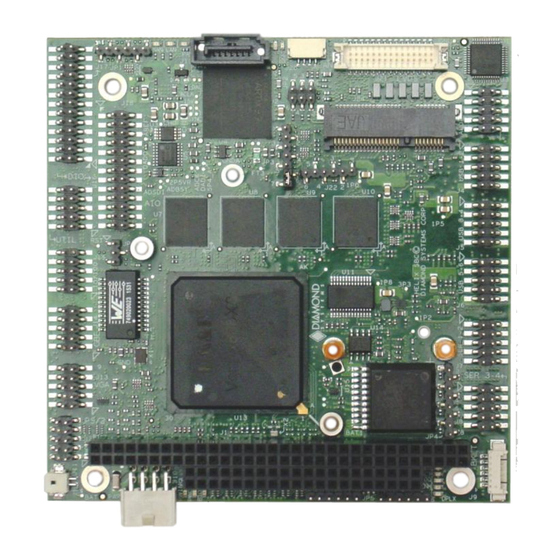
Page 17: Board Layout
5. BOARD LAYOUT Block 3 Block 4 Block 1 Block 2 Figure 3: Board Layout www.diamondsystems.com Helix User Manual Revision A.02 Page 17... -
Page 18: I/O Connectors, Jumpers And Led Summary
LVDS LCD LED Block 4 JTAG for FPGA LED (Left one in DAQ LED the block) SATA Power Connector LED (Right one FPGA DONE in the block) PCIe MiniCard / mSATA Processor JTAG www.diamondsystems.com Helix User Manual Revision A.02 Page 18... -
Page 19: I/O Connectors
6.1.1 PC/104 (J1, J2) The Helix SBC includes the non-stack through / short pin 8-bit and 16-bit PC/104 connectors on the top side in the standard position as described by the latest revision of the PC/104 specification. Note: On the 64-pin connector J1, the leftmost pins are numbered 1. On the 40-pin connector J2, the leftmost pins are numbered 0. -
Page 20: Audio (J3)
There are two serial port connectors J7 and J8, supporting two ports per connector. Serial ports 1-2 support only RS-232 mode. Serial ports 3-4 support RS-232/485/422 modes. RS-232 RTS1 CTS1 RTS2 CTS2 RS-422 TX1+ TX1- RX1+ RX1- TX2+ TX2- RX2+ RX2- www.diamondsystems.com Helix User Manual Revision A.02 Page 20... -
Page 21: Lcd Backlight (J9)
Connector Type: Connector used is IPL1-104-01-L-D-RA-K. 6.1.7 External Battery (J11) Connector J11 is available for use with an external battery. VBAT Ground VBAT = +3.3V Connector Type: Hirose right-angle friction lock pin header. DF13A-2P-1.25H www.diamondsystems.com Helix User Manual Revision A.02 Page 21... -
Page 22: Ps/2 Keyboard And Mouse (J12)
There are two on board connectors for Ethernet – one for 10/100 and one for 10/100/1000. 10/100/1000 Ethernet (J14) Connector Type: Standard 2mm dual row straight pin header. 10/100 Ethernet (J15) Link LED Ground 100 LED Connector Type: Standard 2mm dual row straight pin header www.diamondsystems.com Helix User Manual Revision A.02 Page 22... -
Page 23: Utility (J16)
The DIO pins on the digital I/O connector provide access to jumper-selectable 3.3V / 5V system voltage rail through a polyswitch resettable fuse. The fuse is rated for ~100mA maximum sustained current. The pinout definition for the DIO connector in Helix SBCs with the full data acquisition circuit (A model) is given below. -
Page 24: Analog I/O (J18)
Vout pin is optimized for the analog outputs; Vin pin is optimized for the analog inputs Dground Digital ground; used for digital circuitry only DIO D2-D0 Digital I/O port D; programmable direction Connector type: Standard 2mm dual row straight pin header. www.diamondsystems.com Helix User Manual Revision A.02 Page 24... -
Page 25: Sata (J19)
D1- Odd D1- Even D2+ Odd D2+ Even D2- Odd D2- Even D3+ Odd D3+ Even D3- Odd D3- Even Ground Ground DDC CLK DDC DATA Connector Type: 30-pin connector from Hirose, DF13A-30DP-1.25V www.diamondsystems.com Helix User Manual Revision A.02 Page 25... -
Page 26: Pcie Minicard / Msata Socket (J24)
SATA 0 TX+ +3.3V +3.3V +3.3V +3.3V WWAN LED- Ground Ground WLAN LED- WPAN LED- +1.5V Pull-up to +3.3V Pull-up to +3.3V +3.3V Connector Type: 52-pin MiniCard, full size, with PCB mount threaded spacers www.diamondsystems.com Helix User Manual Revision A.02 Page 26... -
Page 27: List Of Connectors
6.2 List Of Connectors The following table provides a summary of all I/O connectors on the Helix SBC. Function Manufacturer Part Number Description Latching Connector Mating Cable 2x4 box header T/H Right angle .1” Power in Samtec IPL1-104-01-L-D-RA-K 6980512 pitch External 2 pos. -
Page 28: I/O Cables
USB 2.0 J4, J5, J6 6981083 PS/2 6981075 Serial ports J7, J8 6981080 Gigabit Ethernet 6981161 10/100 Ethernet 6981076 Audio 6981169 Utility 6981084 6980515 Analog I/O 6980515 Digital I/O 6981182 6989101 SATA www.diamondsystems.com Helix User Manual Revision A.02 Page 28... -
Page 29: Jumper Description
Figure 4: Default Jumper Locations Jumper Description Digital VIO CAN Termination Miscellaneous: SATA DOM, Boot Delay, Battery Disconnect, Single Channel LCD RS-422/485 Termination LVDS Backlight & LVDS VDD IRQ Selection www.diamondsystems.com Helix User Manual Revision A.02 Page 29... -
Page 30: Digital Io (Jp1)
Low to GND) as this voltage is tied to the input voltage to the DAQ circuits. 8.2 CAN Termination (JP2) Jumper block JP2 is used to enable 120 Ohm CAN termination. Figure 6: Jumper Block JP3 120 Ohm Termination Enabled Disabled www.diamondsystems.com Helix User Manual Revision A.02 Page 30... -
Page 31: Miscellaneous (Jp3)
BAT Jumper in JP3 can be removed to prevent the RTC battery from draining during long term storage. The jumper should be inserted for normal operation. Description Battery power is disconnected to avoid drainage RTC battery power is enabled www.diamondsystems.com Helix User Manual Revision A.02 Page 31... -
Page 32: Rs-422/485 Termination (Jp4)
Single channel LCD By default, Helix supports dual channel LVDS displays. To support a single channel LVDS LCD, a jumper should be inserted in position LVDS. LVDS Description Dual channel LCD is used Single channel LCD is used 8.4 RS-422/485 Termination (JP4) Jumper JP4 is used to enable 120 Ohm termination for serial ports in RS-485 and RS-422 modes. -
Page 33: Lvds Backlight And Lvds Vdd (Jp5)
Available options are +5V and +12V from the main power supply input. +12V is not used by any circuit on the Helix SBC. +12V is needed only for the LCD backlight, and the backlight is to be powered via the backlight power connector J9, hence +12V is supplied on the main power input connector along with +5V. -
Page 34: Bios Key Features
9. BIOS KEY FEATURES The Helix SBC BIOS provides access to many valuable features. These instructions show how to enter the BIOS and set up features. 9.1 Entering the BIOS The BIOS may be entered during startup by pressing the DEL key on an attached keyboard. Press the key repeatedly soon after a power-on or reset until the BIOS screen appears. -
Page 35: Led
9.9 Serial Port Configuration The Helix SBC supports four serial ports. Ports 1 and 2 support RS-232 functionality. Ports 3 and 4 support RS- 232/422/485 functionality. Ports 3 and 4 can be configured from the BIOS GUI. In the BIOS setup go to the Advanced menu and select the Serial/Parallel port configuration. -
Page 36: Getting Started
10. GETTING STARTED This section describes the steps needed to get your Helix SBC up and running and assumes that you also have a Helix Development Kit or Helix Cable Kit. The Cable Kit includes all cables needed for most I/O, except the LCD and backlight. -
Page 37: Installing Os And Booting
The following steps describe how to install an operating system from an external SATA hard disk drive. An external SATA HDD requires power and data cables to be connected to it. The data cable connects the Helix SBC to the HDD. Power to the HDD should be sourced from an external power supply. -
Page 38: Video Features
To set the LCD as the primary display, connect the LCD to the Helix SBC before power on. Do not connect the VGA cable. Boot the SBC to Windows 7 OS and check the graphics utility. The LCD should be enabled under the display devices menu. -
Page 39: Changing Lcd Resolution
11.4 Changing LCD Resolution The LCD resolution supported by Helix is defined in the VBIOS file embedded in the BIOS image. The VBIOS file can store up to five LCD resolutions, one of which will be active at a time. The default BIOS will have support for the following resolutions: 640x480, 800x480, 800x600, 1024x600, and 1920x1080. - Page 40 Note: If your LCD resolution is not in the list, please send the LCD datasheet to Diamond Systems for new VBIOS ROM. Choose the desired LCD resolution from the menu LCD Panel Default Setting. By default 1920x1080 is the standard LCD setting set in the Helix BIOS. Save the new VBIOS. www.diamondsystems.com Helix User Manual Revision A.02...
-
Page 41: Step 2: Integrate The Vbios With The Bios File
MMTOOL.EXE. The following items are required to modify the BIOS image: 1. PC with MMTOOL software 2. Existing Helix BIOS image 3. Helios LCD VBIOS file 4. Bootable USB memory stick with DOS 5. ANYBIOS utility saved in DOS bootable USB memory stick. - Page 42 4. Go to Replace, Load new VBIOS file to be integrated. Select the VBIOS module on 17F3:2015 indicated by arrow, and press “Replace.” 5. Save the new BIOS. Refer to the section “Upgrading BIOS Using DOS Utility” for instructions on how to flash the new BIOS. www.diamondsystems.com Helix User Manual Revision A.02 Page 42...
-
Page 43: Serial Ports And System Console
BIOS configuration, console redirection is disabled. A serial port on the remote PC can be connected to the serial port on Helix with a null modem cable. A null modem cable has a DB9 female connector at each end and swaps the TX and RX signals from one end to the other, so that two DTE devices can communicate directly with each other. -
Page 44: Mass Storage
13. MASS STORAGE The Helix SBC can use a wide variety of mass storage options, both on-board and off-board. These options include external SATA hard disk drives, a board-mounted SATA DOM or mSATA flashdisks, or external USB hard drives. 13.1 Flashdisk Models and Capacities Diamond Systems offers the following extended temperature SATA DOM and mSATA flashdisks for use with Helix SBCs. -
Page 45: Utility Connector Features
14.2 Reset The Helix SBC can be reset using the Reset- signal on pin 1 of the utility connector. Reset- is an active low signal and must be connected to Ground (Pin 3 or pin 9) to reset the device. The typical reset period is 10mS. Reset- has a weak pull up resistor (100K Ohm) to 3.3V on board. -
Page 46: A Model Data Acquisition Circuit
15.1 Features Helix “A” models include a complete data acquisition circuit with a combination of analog and digital I/O features. The circuit controller is an FPGA that interfaces to the Vortex86DX3 processor via the SPI bus for data I/O and via the ISA bus for interrupt operation. -
Page 47: Block Diagram
15.3.1 A/D Circuit Overview Helix “A” models include an analog input circuit based on the LTC1859 16-bit A/D converter, or ADC. The LTC1859 is capable of operating at up to 100,000 samples per second in total, either on a single channel or on any number of channels. -
Page 48: A/D Channel Selection, Sampling, And Timing
ISA bus. The software can then respond to the interrupt and read out a large number of samples all at once. The Diamond Systems Universal Driver software provides full support for high speed A/D sampling with FIFO and interrupt support. Please refer to that user manual for operating details. -
Page 49: A/D Operation
Significant Bit). The resolution is always 16 bits, but the value of 1 LSB will vary with the input range. Polarity Input Range Resolution (1LSB) Bipolar ±10V 305µV Bipolar ±5V 153µV Unipolar 0 - 10V 153µV Unipolar 0 - 5V 76µV www.diamondsystems.com Helix User Manual Revision A.02 Page 49... -
Page 50: Input Range Selection
5V or 10V. Example: For unipolar input range 0-5V, full-scale input voltage = 5V. For an A/D value of 17761: Input voltage = 17761 / 65536 * 5V = 1.355V www.diamondsystems.com Helix User Manual Revision A.02 Page 50... -
Page 51: Measurement Accuracy And Calibration
The higher the output impedance of the input signal, the greater the error will be. Conversely, the higher the input impedance of the A/D circuit, the lower the error will be. Helix uses high impedance, ultra-low- offset buffer op amps to boost the input impedance to well over 10 GigOhms (the input impedance is calculated based on the specified input current of 75pA). -
Page 52: Digital-To-Analog Circuit
15.4 Digital-to-Analog Circuit 15.4.1 Overview The Helix data acquisition circuit uses a 16-bit D/A converter. This means that all output voltages are defined by a 16-bit binary number, or D/A code, ranging from 0 to 65535 (2 -1), or binary 0000 0000 0000 0000 to 1111 1111 1111 1111. -
Page 53: D/A Conversion Formula
To minimize the size and cost of the D/A circuit while still providing reasonable performance, the D/A circuit on Helix does not provide calibration features to eliminate these errors. Instead the circuit was designed to minimize the inherent offset, gain, and drift characteristics. The specifications at the end of this manual indicate the worst case offset, gain, and temperature drift errors in the circuit. -
Page 54: Digital I/O Features
The edge detection circuit on Helix contains an enable register, a polarity register, and a status register. The programmer can specify which bits will be active with the enable register and which transition to detect on each bit (0 to 1 or 1 to 0) with the polarity register. -
Page 55: Support For Special Functions
15.6 Counter/Timer Features 15.6.1 Overview Helix “A” models include 8 32-bit counter/timers with a wide array of features and programmability. Both up and down counting are supported, and the clock for each counter can be selected from an internal 50MHz or 1MHz clock or an external digital signal. -
Page 56: Counter Commands
The counters are configured and managed with a series of commands. These commands are implemented in the Diamond Systems Universal Driver software. Commands may operate on either a single counter or any combination of counters simultaneously using a user-defined selection mask. -
Page 57: Pulse Width Modulator Features
15.7.1 Overview Helix “A” models include 4 24-bit pulse width modulator circuits (PWMs). These circuits can be programmed to produce an output square wave up to 25MHz with a duty cycle anywhere from 0% to 100% (these limits are of course DC signals). -
Page 58: Interrupt Operation
The programmer must find the ideal balance between processor load and response time. The primary host interface for the Helix “A” model data acquisition circuit is the SPI bus. However the SPI bus does not provide a means to support interrupt operation. Therefore Helix “A” models provide the ability to generate interrupts on the ISA bus. -
Page 59: D" Model Digital I/O Circuit
16.1 Features Helix “D” models provide digital I/O coming from the DX3 processor. The digital I/O consists of 16 I/O lines organized as two 8-bit ports A and B. These ports utilize the same I/O circuitry as the “A” model. They utilize 8-bit bidirectional buffers for enhanced current drive and protection from faulty connections. -
Page 60: Configuration And Programming
Don’t care, these bits are not used For all bits, 1 = output, 0 = input. All bits reset / power-up to 0. The 4 upper bits in register 0x9A must be set to 1. www.diamondsystems.com Helix User Manual Revision A.02 Page 60... -
Page 61: Programming Instructions
Helix offers stackable I/O expansion over the 8/16-bit ISA bus. Since a provision is provided to mount SATA DOM on the top side of the board, PC/104 boards can be stacked on the bottom side of Helix. The ISA interface supports DMA. -
Page 62: Software Driver Overview
Development kits contain a SATA DOM installed with either Windows Embedded 7 or Linux. All the necessary I/O drivers are also available as part of the Development Kit. Please contact Diamond Systems for more details. Some of the drivers that are required with the Windows 7 operating system are given below. These drivers are available for download from Diamond Systems’... -
Page 63: Specifications
7.0W idle (without DAQ) 9.5W idle (with DAQ) Dimensions 4.0" x 4.0" (101.5mm x 101.5mm) Weight 2.5oz (70.8g) with heat sink Operating temperature -40°C to +85°C (-40°F to +185°F) Shock MIL-STD-202G compatible Vibration MIL-STD-202G compatible RoHS Compliant MTBF www.diamondsystems.com Helix User Manual Revision A.02 Page 63... - Page 64 Input voltage Input current Output voltage +3.3V Output current PWMs 4 24-bit pulse width modulators, 0-100% duty cycle Watchdog timer Programmable watchdog timer 0-255 seconds Counter/Timers 8 32-bit counter/timers A/D pacer clock www.diamondsystems.com Helix User Manual Revision A.02 Page 64...
Need help?
Do you have a question about the HELIX and is the answer not in the manual?
Questions and answers