Table of Contents
Advertisement
Quick Links
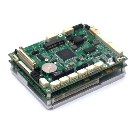
VEGA Single Board Computer
COM Express Form-factor Embedded Computer with
Configurable COM Express CPU and Integrated Data
Revision
Date
A.00
11/4/2014
A.01
11/19/2015
FOR TECHNICAL SUPPORT
PLEASE CONTACT:
support@diamondsystems.com
Acquisition
Comment
Initial release
Minor revisions
Copyright
Diamond Systems Corp
555 Ellis Street
Mountain View, CA 94043 USA
Tel 1-650-810-2500
Fax 1-650-810-2525
www.diamondsystems.com
2015
Advertisement
Table of Contents

Related Manuals for Diamond Systems VEGA


Summary of Contents for Diamond Systems VEGA
- Page 1 VEGA Single Board Computer COM Express Form-factor Embedded Computer with Configurable COM Express CPU and Integrated Data Acquisition Revision Date Comment A.00 11/4/2014 Initial release A.01 11/19/2015 Minor revisions Copyright 2015 FOR TECHNICAL SUPPORT Diamond Systems Corp PLEASE CONTACT: 555 Ellis Street Mountain View, CA 94043 USA support@diamondsystems.com...
-
Page 2: Table Of Contents
BIOS ................................28 BIOS Main Setup Screen ........................... 28 Advanced Settings ............................29 Chipset Settings............................32 Boot Settings .............................. 35 Security Settings ............................36 Save & Exit Settings ........................... 37 Analog I/O Operation ............................. 38 www.diamondsystems.com Vega SBC User Manual A.01 Page... - Page 3 10. Counter/Timer Operation ..........................53 11. FlashDisk Modules ............................55 11.1 Installing the Flashdisk Module ........................55 12. Specifications ..............................56 12.1 System ................................ 56 12.2 Data Acquisition ............................56 12.3 Mechanical & Environmental ........................57 www.diamondsystems.com Vega SBC User Manual A.01 Page...
-
Page 4: Important Safe-Handling Information
The list here describes common causes of failure found on boards returned to Diamond Systems for repair. This information is provided as a source of advice to help you prevent damaging your Diamond (or any vendor’s) embedded computer boards. - Page 5 Overvoltage on digital I/O line — The digital circuitry can be damaged if a digital I/O signal is connected to a voltage above the Vega’s maximum specified voltage. On most of our boards the acceptable range of voltages connected to digital I/O signals is 0-5V, and they can withstand about 0.5V beyond that (-0.5 to 5.5V) before being damaged.
-
Page 6: Introduction
I/O expansion modules to tune system functionality to the application’s precise requirements. Vega is offered in a range of models that vary according to the choice of COM Express CPU module, on-board SO-DIMM SDRAM capacity, variable-input DC/DC supply, and optional data acquisition circuitry. -
Page 7: Vega Baseboard Features
COM Express dimensions and mounting holes 1.2 Operating System Compatibility Vega’s operating system compatibility depends on both the Vega baseboard and the specific COM Express CPU module attached to it. The baseboard has been qualified for use with the following operating systems: Windows Embedded Standard 7, Windows Embedded CE Linux v2.6.23... -
Page 8: Vega Sbc Models
1.3 Vega SBC Models Several models of the Vega SBC are available with different COM Express CPU modules, memory, and optional on-board data acquisition circuitry. These models are described in the following table. Model Number Description VEGA-3612QE-8GA Vega SBC, 2.1GHz Intel Core i7-3612QE CPU, 8GB RAM, full data acquisition VEGA-3612QE-8GN Vega SBC, 2.1GHz Intel Core i7-3612QE CPU, 8GB RAM, no data acquisition... -
Page 9: Cable Kit
1.5 Cable Kit The Vega cable kit (part number (CK-VEGA-01) provides convenient access to all of Vega’s I/O features. The kit’s cables are shown in the photo below and are identified in the table that follows. The components of the Vega Cable Kit are listed below. -
Page 10: Functional Overview
2. FUNCTIONAL OVERVIEW 2.1 Block Diagrams Figure 1 shows the functional blocks of the Vega I/O baseboard. As indicated in the block diagram, the baseboard circuitry primarily comprises the data acquisition subsystem, Gigabit Ethernet controller, DC/DC power supply, and I/O interfaces. The COM Express module integrates to the I/O baseboard via connectors A/B and C/D and provides the system’s core embedded PC functionality. - Page 11 Figure 2: Typical COM Express CPU Module Functional Block Diagram www.diamondsystems.com Vega SBC User Manual A.01 Page...
-
Page 12: Functional Overview
CPU Core Vega’s core embedded computer is based on a COM Express CPU offering a choice of an Intel® 2.1GHz Core i7- 3612QE or 1.4GHz Celeron 827E CPU. The COM Express COM module provides the standard PC I/O for the Vega system as described in the following sections. -
Page 13: Data Acquisition
I/O Expansion The Vega baseboard supports a standard PCIe MiniCard socket. It uses the x1 PCIe (Port 1) from the COM Express attached processor. One of the USB ports (Port 1) from the COM Express connector is terminated to the PCIe MiniCard socket. -
Page 14: Bios
The Vega COM Express CPU module’s BIOS ROM provides a wide range of configuration options. When you power up the Vega SBC, you can immediately enter the BIOS “Setup” utility (prior to OS boot-up) in order to adjust BIOS settings to match your system’s peripheral devices and other requirements, and to configure various other hardware and software parameters. -
Page 15: Board Layout
2.4 Board Layout Figure 3 illustrates the location of connectors and jumpers on the top side of the Vega I/O baseboard. Figure 4 illustrates the location of connectors on the COM Express CPU. The COM Express CPU module attaches on the baseboard’s bottom side. - Page 16 Figure 4: COM Express CPU Bottom View www.diamondsystems.com Vega SBC User Manual A.01 Page...
-
Page 17: Interface Connector Summary
— COM Express CPU module or Vega I/O baseboard — provides the electronics associated with each connector. Signal functions relating to all of Vega’s interfaces connectors are discussed in greater detail in Section 6. Connector Associated... -
Page 18: Configuration Jumper Summary
2.6 Configuration Jumper Summary The Vega baseboard’s configuration jumper blocks are listed below. Details regarding the use of these jumpers appear in Section 5 of this document. Jumper Description Digital I/O output resistors and FPGA base address RS-422/485 termination resistors... -
Page 19: Analog I/O (J8)
3.3 Analog I/O (J8) Connector J8 provides the analog I/O signals from the on-board data acquisition circuitry. There are no ESD protection diodes for these signals. This funtionality is only available on Vega A models. VIN0 VIN8 VIN1 VIN9 VIN2... -
Page 20: Gigabit Ethernet (J11, J12)
3.5 Gigabit Ethernet (J11, J12) The Vega SBC provides two Gigabit Ethernet ports, one provided directly from the COM Express COM CPU (J12) and the other generated on the Vega I/O baseboard (J11). The connector pinout for both ports is identical. -
Page 21: Usb (J17, J18)
3.8 USB (J17, J18) Connectors J17 and J18 provide access to Vega’s four USB 2.0 ports. Connector J17 has USB ports 1 and 2, and connector J18 has USB ports 3 and 4. The pinout for both connectors is identical. The shield pin on each connector is tied to system ground. -
Page 22: Lcd Panel (Lvds Interface) (J20)
Brightness, 0-5VDC variable; 0V = max, 5V = min Connector description: Hdr, 1x6 ST 1.25mm Shroud TH Connector part number: Molex, 53261-0671 Cable-mount socket: Molex, 51021-0600 or equivalent Terminals: Molex, 50058 / 50079 series or equivalent www.diamondsystems.com Vega SBC User Manual A.01 Page... -
Page 23: Audio (J22)
Connector description: CONN,2x5P,1.5MM,LOCK,SH,R/A,SMT Connector part number: JST, SM10B-ZPDSS-TF 3.13 EMX I/O Expansion (J23) Connector J23 allows one EMX compliant I/O expansion module to be plugged in to the Vega I/O baseboard. The connector pinout follows the EMX standard. USB2+ SATA-R+... -
Page 24: External Battery (J24)
The VGA connector, J28, has the VGA signals terminated to it from the SDVO to VGA converter. A VGA monitor can be connected to this. VGA GND GREEN VGA GND BLUE VGA GND HSYNC VSYNC DDC DATA DDC CLK Connector description: CONN,2x7P,1.5MM,LOCK,SH,R/A,SMT Connector part number: JST, SM14B-ZPDSS-TF www.diamondsystems.com Vega SBC User Manual A.01 Page... -
Page 25: Input Power (J29)
3.17 Input Power (J29) J29 is used to provide power to the Vega single board computer. +7 to +36V PGND +7 to +36V PGND +7 to +36V PGND +7 to +36V PGND 5V_STBY PS_ON# Connector description: CONN, 2x5pin, 2.54mm, Shroud, RA, TH Connector part number: Samtec, IPL1-105-01-L-D-RA-K 3.18 Display Port (DP1) -
Page 26: Configuration Jumper Details
4. CONFIGURATION JUMPER DETAILS This section describes the use of the Vega I/O baseboard’s configuration jumper options and indicates the default settings when appropriate. 4.1 Digital I/O Output Resistors and FPGA Base Address (JP1) Jumper JP1 is to set the digital I/O output 10K resistors to either pull-up or pull-down. The default is no jumper, meaning neither pull-up nor pull-down is selected. -
Page 27: Lcd Supply Voltage (Jp3)
The default settings are normal scan and Map-A. Jumper on No Jumper Jumper Pins 1 & 2 Reverse scan Normal scan (default) 3 & 4 Map-B Map-A (default) Default setting: Jumpers on pins 1&2, 3&4 www.diamondsystems.com Vega SBC User Manual A.01 Page... -
Page 28: Bios
The AMI BIOS provides a setup utility program for specifying the system configurations and settings which are stored in the BIOS ROM of the system. When you power on the Vega SBC, the AMI BIOS is immediately activated. After entering the BIOS setup utility, use the left and right arrow keys to highlight a specifiic configuration screen from the top menu bar. -
Page 29: Advanced Settings
Enable for Windows XP and Linux, disable for other Oss Limit CPUID Maximum: Enable or disable the Limit CPUID Maximum Intel Virtualization Technology: Enable or disable virtualization When enabled, a VMM can utilize the additional hardware capabilities www.diamondsystems.com Vega SBC User Manual A.01 Page... - Page 30 Enable or disable the serial port 1 Change serial port 1’s port address and interrupt address Change Settings: Device Mode: Set to Standard Serial Port Mode, IrDA 1.0 (HP SIR) Mode, or ASKIR Mode www.diamondsystems.com Vega SBC User Manual A.01 Page...
- Page 31 Enable or disable the CPU C3 (ACPI C2) report to the OS CPU C6 Report: Enable or disable the CPU C6 (ACPI C3) report to the OS CPU C7 Report: Enable or disable the CPU C7 (ACPI C3) report to the OS www.diamondsystems.com Vega SBC User Manual A.01 Page...
-
Page 32: Chipset Settings
Set the DVMT 5.0 fixed graphics memory size to between 0MB and 512MB DVMT Total Gfx Mem: Set the total graphics memory size to 128MB, 256MB or MAX Gfx Low Power Mode: Enable or disable low power mode, applicable for SFF only www.diamondsystems.com Vega SBC User Manual A.01 Page... - Page 33 RMT Crosser Support: Enable of disable RmtCrosserEnable support MRC Fast Boot: Enable or disable MRC fast boot Force Cold Reset: Force cold reset or choose MRC cold reset mode If ME 5.0MB is present, Force Cold Reset is required www.diamondsystems.com Vega SBC User Manual A.01 Page...
- Page 34 Enable or disable Extended Synch on SB side of the DMI Link Subtractive Decode: Enable or disable Subtractive Decode PCI Express Root Port X Sub-Menu (same for all ports 1-8) Control the PCI Express Root Port for each port www.diamondsystems.com Vega SBC User Manual A.01 Page...
-
Page 35: Boot Settings
Quiet Boot: Enable or disable the screen display when the system boots Boot Option Priorities Select the boot sequence of the hard drives Hard Drive BBS Priorities Set the hard drive boot priority www.diamondsystems.com Vega SBC User Manual A.01 Page... -
Page 36: Security Settings
5.5 Security Settings Administrator Password Set or change an eight character administrator password To disable a password, enter a blank password www.diamondsystems.com Vega SBC User Manual A.01 Page... -
Page 37: Save & Exit Settings
5.6 Save & Exit Settings www.diamondsystems.com Vega SBC User Manual A.01 Page... -
Page 38: Analog I/O Operation
6.1 A/D Input Ranges and Resolution The Vega baseboard uses a 16-bit A/D converter. This means that the analog input voltage can be measured to the precision of a 16-bit binary number. The maximum value of a 16-bit binary number is 2 - 1, so the full range of numerical values that you can get from a Vega baseboard analog input channel is 0 - 65535. -
Page 39: Conversion Formulas
Full scale input voltage): A/D Code Input Voltage Input Voltage for Symbolic Formula 5V Range -32768 -5.0000V -32767 + 1 LSB -4.9998V -1 LSB -0.00015V 0.0000V +1 LSB 0.00015V 32767 - 1 LSB 4.9998V www.diamondsystems.com Vega SBC User Manual A.01 Page... -
Page 40: A/D Control Signals
MUXEN1/0 is high when the mux enable outputs are MUXEN[1:0]=10b (i.e. channels 15 to 8 are selected). It is low when MUXEN[1:0]=01b (i.e. channels 7 to 0 are selected). ADCH<3:0> = < 0, PADCH2, PADCH1, PADCH0> any of 8 channels in Differential mode. www.diamondsystems.com Vega SBC User Manual A.01 Page... - Page 41 ADBUSY is an input connected the BUSY output from the ADC. The BUSY output falls when a conversion is started and remains low until the conversion is completed and the data is latched into the output shift register. www.diamondsystems.com Vega SBC User Manual A.01 Page...
-
Page 42: A/D Sampling Methods
6.5.1 Sampling Modes There are several different A/D sampling modes available on a Vega baseboard. The desired mode is selected with the FIFOEN and SCANEN bits at the FIFO Control register (Base+7), and the ADINTE bit in the Interrupt Control register (Base+9). -
Page 43: Fifo Description
On Vega, this number is programmable using the FIFO Threshold register (Base+6). The usual value is 1/2 the maximum FIFO depth, or 1024 samples. Therefore, the maximum interrupt rate for Vega is reduced to 996 per second, which is easily sustainable on any popular operating system. -
Page 44: Scan Sampling
Initiate an A/D conversion Wait for the conversion to finish Read the data from the board Convert the numerical data to a meaningful value Each of these steps is discussed in detail on the following pages. www.diamondsystems.com Vega SBC User Manual A.01 Page... -
Page 45: Select The Input Channel
6.6.1 Select the Input Channel The Vega baseboard contains a channel counter circuit that controls which channel is sampled on each A/D conversion command. The circuit uses two channel numbers called the low channel and high channel. These are stored in the A/D Low Channel and A/D High Channel registers (Base+2 and Base+3). The circuit starts at the low channel and automatically increments after each A/D conversion until the high channel is reached. -
Page 46: Select The Input Range
Alternatively, the value can be read as one 16-bit value, which is preferred since this method increases overall system bandwidth while reading data from the FIFO. For example: Data = inpw(base); // Where the MSB and LSB are read in one access www.diamondsystems.com Vega SBC User Manual A.01 Page... -
Page 47: Convert The Numerical Data To A Meaningful Value
A/D channel range (low channel, high channel). On Vega, the channel numbers range from 0 to 31. Some channel numbers may not be available, depending on the single-ended/differential configuration mode as explained on page 11. During interrupt- based A/D conversions, the channels being sampled must be consecutive in number. To sample only a single channel, set the low channel and high channel to the same channel number. -
Page 48: D/A Conversion
10b. If it is set to 0, then MUXEN[1:0] is set to 01b. If the CALMUX bit in page 1 is set (‘1’), CALEN goes high and all other MUXENx bits go low (i.e. there is no output from either mux). Otherwise CALEN is low. www.diamondsystems.com Vega SBC User Manual A.01 Page... - Page 49 They serve no functional purpose other than debug. Their values are also reflected in the corresponding read- back bits at base+6. Please refer to Diamond Systems’ Universal Driver 7.0 User Manual for information on using and programming the analog I/O.
-
Page 50: Pulse Width Modulators
7. PULSE WIDTH MODULATORS Vega offers four 24-bit pulse width modulator (PWM) circuits. The PWMs are programmed using a 24-bit PWM data register PWMD23-0 and an 8-bit command register PWCMD3-0 + PWM2-0 + PWMCD. Each PWM consists of a pair of 24-bit down counters named C0 and C1. The C1 counter defines the duty cycle (active portion of the signal), and the C0 counter defines the period of the signal. -
Page 51: Waveform Generator
To make the pulse appear on the output pin, command 0011 must additionally be executed, otherwise the output will be held in inactive mode (the opposite of the selected polarity for the PWM output). Please refer to Diamond Systems’ Universal Driver 7.0 User Manual for information on using and programming the pulse width modulators. -
Page 52: Digital I/O Operation
9. DIGITAL I/O OPERATION Vega contains 30 3.3V digital I/O lines organized in four groups: A, B, C & D. Groups A to C consist of eight signals each and port D consist of only 6 signals. The direction of each port is independently programmable. All bits on all ports are individually programmable for input or output with register bits DIRA7-0, DIRB7-0, DIRD7-0, and DIRD7-0. -
Page 53: Counter/Timer Operation
Clk1 Input Out0 Output Please refer to Diamond Systems’ Universal Driver 7.0 User Manual for information on using and programming the digital I/O. 10. COUNTER/TIMER OPERATION Vega offers eight 32-bit counter/timers with programmable functions. The counters are programmed using a command register at address 5 in the counter block, a counter number register at address 4, and a 32-bit data register CTRD31-0 at addresses 0-3. - Page 54 Reset means all registers and settings are cleared to zero. A command of 0xFF will reset all counters (although the precise command is 0xF1).. Please refer to Diamond Systems’ Universal Driver 7.0 User Manual for information on using and programming the counter/timers.
-
Page 55: Flashdisk Modules
11. FLASHDISK MODULES Vega is designed to accommodate an optional solid-state mSATA or USB flashdisk module. These modules contain up to 64GB of solid-state non-volatile memory that operates like a hard drive without requiring additional driver software support. Note that the mSATA flashdrive and PCIe MiniCard modules share the same socket. -
Page 56: Specifications
Expansion socket: PCIe MiniCard socket Bus interface: EMX (PCIe) +7-36V DC/DC on-board power supply Power consumption: VEGA-3612QE-4GA -- 14.52W at 12V typical VEGA-3517UE-4GA -- 13.93W at 12V typical VEGA-827E-2GA -- 14.7W at 12V typical 12.2 Data Acquisition 16 16-bit analog inputs Inputs user-configurable as: 16 single-ended, 8 differential, or 16 SE + 8 DI Bipolar ranges: ±10V, ±5V, ±2.5V, ±1.25V... -
Page 57: Mechanical & Environmental
Shock: MIL-STD-202G, Method 213B compatible Vibration: MIL-STD-202G, Method 214A compatible Dimensions: Vega Core i-7 models -- 4.92” x 3.74” x 1.4” (125mm x 95mm x 35.7mm) MTBF: Vega baseboard with DAQ – 277,880 hours @ 20 Core i7-3612QE & Core i7-3517UE COMs – 146,217 hours at 25 Celeron 827E COM –...
Need help?
Do you have a question about the VEGA and is the answer not in the manual?
Questions and answers