
Related Manuals for Aaeon GENE-BT04


Summary of Contents for Aaeon GENE-BT04
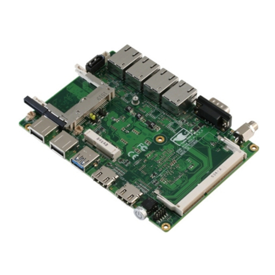
- Page 1 GENE-BT04 3.5” Subcompact Board User’s Manual 1 Last Updated: November 9, 2015...
-
Page 2: Copyright Notice
AAEON assumes no liabilities resulting from errors or omissions in this document, or from the use of the information contained herein. AAEON reserves the right to make changes in the product design without notice to its users. - Page 3 Acknowledgement All other products’ name or trademarks are properties of their respective owners. ® Microsoft Windows is a registered trademark of Microsoft Corp. ITE is a trademark of Integrated Technology Express, Inc. IBM, PC/AT, PS/2, and VGA are trademarks of International Business Machines ...
- Page 4 Before setting up your product, please make sure the following items have been shipped: Item Quantity GENE-BT04 (with heat spreader) Product DVD with User’s Manual (in pdf) and drivers If any of these items are missing or damaged, please contact your distributor or sales representative immediately.
- Page 5 (if any), its specifications, dimensions, jumper/connector settings/definitions, and driver installation instructions (if any), to facilitate users in setting up their product. Users may refer to the AAEON.com for the latest version of this document. Preface...
- Page 6 Safety Precautions Please read the following safety instructions carefully. It is advised that you keep this manual for future references All cautions and warnings on the device should be noted. Make sure the power source matches the power rating of the device. Position the power cord so that people cannot step on it.
- Page 7 If any of the following situations arises, please the contact our service personnel: Damaged power cord or plug Liquid intrusion to the device iii. Exposure to moisture Device is not working as expected or in a manner as described in this manual The device is dropped or damaged Any obvious signs of damage displayed on the device...
- Page 8 FCC Statement This device complies with Part 15 FCC Rules. Operation is subject to the following two conditions: (1) this device may not cause harmful interference, and (2) this device must accept any interference received including interference that may cause undesired operation.
- Page 9 China RoHS Requirements (CN) 产品中有毒有害物质或元素名称及含量 AAEON Main Board/ Daughter Board/ Backplane 有毒有害物质或元素 部件名称 铅 汞 镉 六价铬 多溴联苯 多溴二苯醚 (Pb) (Hg) (Cd) (Cr(VI)) (PBB) (PBDE) 印刷电路板 × ○ ○ ○ ○ ○ 及其电子组件 外部信号 × ○ ○ ○ ○ ○...
- Page 10 China RoHS Requirement (EN) Poisonous or Hazardous Substances or Elements in Products AAEON Main Board/ Daughter Board/ Backplane Poisonous or Hazardous Substances or Elements Hexavalent Polybrominated Polybrominated Component Lead Mercury Cadmium Chromium Biphenyls Diphenyl Ethers (Pb) (Hg) (Cd) (Cr(VI)) (PBB) (PBDE) PCB &...
-
Page 11: Table Of Contents
Table of Contents Chapter 1 - Product Specifications ..................1 Specifications ......................2 Chapter 2 – Hardware Information ..................4 Dimensions ....................... 5 Jumpers and Connectors ..................7 Block Diagram ......................9 List of Jumpers ....................... 10 2.5.1 Clear CMOS Jumper (CN12, Pin 1,3,5) ........11 2.5.2 Auto Power Button Enable/Disable Selection (JP12, Pin 2,4,6) 2.5.3... - Page 12 2.5.15 HDMI Port 1 and 2 (CN20/ 21) ........... 23 2.5.16 LPC Port (CN22) ................24 2.5.17 SPI Programming Header (CN23) ..........25 Chapter 3 - AMI BIOS Setup ....................26 System Test and Initialization ................27 AMI BIOS Setup ..................... 28 Setup submenu: Main ..................
- Page 13 Chapter 4 – Drivers Installation .................... 56 Product CD/DVD ....................57 Appendix A - Watchdog Timer Programming ..............59 Watchdog Timer Registers .................. 60 Watchdog Sample Program ................61 Appendix B - I/O Information ....................64 I/O Address Map ....................65 Memory Address Map ..................
-
Page 14: Chapter 1 - Product Specifications
Chapter 1 Chapter 1 - Product Specifications... -
Page 15: Specifications
Specifications System 3.5” Form Factor ® Intel AtomTM N2807/ J1900 SoC (1.58/ 2.0 Processor GHz) DDR3L 1333 MHz SODIMM x 1, up to 8GB System Memory ® Intel AtomTM N2807/ J1900 SoC Chipset Fintek 81801U I/O Chipset ... - Page 16 CD & FCC class A (pre-scan only) Display ® Chipset Intel AtomTM N2807/ J1900 SoC ® Engine Intel AtomTM N2807/ J1900 SoC Up to 2560 x 1200 for HDMI Resolution HDMI x 2 (HDMI1 with audio, HDMI2 without) Output Interface ...
-
Page 17: Chapter 2 - Hardware Information
Chapter 2 Chapter 2 – Hardware Information... -
Page 18: Dimensions
Dimensions Component Side Chapter 2 – Hardware Information... - Page 19 Solder Side Chapter 2 – Hardware Information...
-
Page 20: Jumpers And Connectors
Jumpers and Connectors Component Side Chapter 2 – Hardware Information... - Page 21 Solder Side Chapter 2 – Hardware Information...
-
Page 22: Block Diagram
Block Diagram Chapter 2 – Hardware Information... -
Page 23: List Of Jumpers
List of Jumpers Please refer to the table below for all of the board’s jumpers that you can configure for your application Label Function CN12 (1,3,5) Clear CMOS Jumper CN12 (2,4,6) Auto Power Button Enable/Disable Selection Push Power Button With Orange LED Chapter 2 –... -
Page 24: Clear Cmos Jumper (Cn12, Pin 1,3,5)
2.5.1 Clear CMOS Jumper (CN12, Pin 1,3,5) Normal (Default) Clear CMOS 2.5.2 Auto Power Button Enable/Disable Selection (JP12, Pin 2,4,6) Disable Enable (Default) 2.5.3 Push POWER Button with Orange LED (SW4) Pin Name Signal Type Signal level +V5S Chapter 2 – Hardware Information... - Page 25 PWRBTN# Chapter 2 – Hardware Information...
-
Page 26: List Of Connectors
List of Connectors Please refer to the table below for all of the board’s connectors that you can configure for your application Label Function COM port RS-232 +12V Input LAN (RJ-45) Port LAN (RJ-45) Port LAN (RJ-45) Port LAN (RJ-45) Port +5V Output for SATA HDD SATA Port DDR3L SO-DIMM Slot... -
Page 27: Com Port Rs-232 (Cn1)
2.5.1 COM Port RS-232 (CN1) Pin Name Signal Type Signal level ± 9V ± 9V ± 9V 2.5.2 +12 V Input (CN2) Pin Name Signal Type Signal Level +12V +12V 2.5.3 LAN Port 1/2/3/4 (RJ-45) (CN3,4,5,6) Chapter 2 – Hardware Information... -
Page 28: Output For Sata Hdd (Cn7)
Pin Name Signal Type Signal Level MDI0+ DIFF MDI0- DIFF MDI1+ DIFF MDI2+ DIFF MDI2- DIFF MDI1- DIFF MDI3+ DIFF MDI3- DIFF 2.5.4 +5 V Output for SATA HDD (CN7) Pin Name Signal Type Signal Level +V5S Chapter 2 – Hardware Information... -
Page 29: Sata Port (Cn8)
2.5.5 SATA Port (CN8) Pin 1 Pin 7 Pin Name Signal Type Signal Level SATA_TXP1 DIFF SATA_TXN1 DIFF SATA_RXN1 DIFF SATA_RXP1 DIFF 2.5.6 DDR3L SODIMM Slot (CN9) Standard specification 2.5.7 Digital I/O Port (CN10) Pin Name Signal Type Signal Level +V5S DIO0 DIO1... -
Page 30: Cfast Card Connector (Cn11)
DIO2 DIO3 2.5.8 CFast Card Connector (CN11) Pin Name Signal Type Signal level SATA_TXP0 DIFF SATA_TXN0 DIFF SATA_RXN0 DIFF SATA_RXP0 DIFF CFD_LED# +3.3V Chapter 2 – Hardware Information... -
Page 31: Minicard Slot (Usb Port2 Only) (Cn13)
+V3.3S +3.3V +V3.3S +3.3V 2.5.9 MiniCard Slot (USB Port2 only) (CN13) Pin Name Signal Type Signal level WAKE_PCIE0#_3P3 +V3.3A +3.3V +V1.5S +1.5V DIFF DIFF Chapter 2 – Hardware Information... - Page 32 Pin Name Signal Type Signal level WL_DISABLE0# +3.3V BUF_PLT_RST# +3.3V DIFF +V3.3A +3.3V DIFF +V1.5S +1.5V SMB_CLK_3P3_FA +3.3V DIFF SMB_DATA_3P3_FA +3.3V DIFF USB_DN2 DIFF USB_DP2 DIFF +V3.3A +3.3V +V3.3A +3.3V Chapter 2 – Hardware Information...
- Page 33 Pin Name Signal Type Signal level +V1.5S +1.5V +V3.3A +3.3V Chapter 2 – Hardware Information...
-
Page 34: Battery (Cn14)
2.5.10 Battery (CN14) Pin Name Signal Type Signal Level +3.3V 3.3V 2.5.11 Buzzer Connector (CN15) Pin Name Signal Type Signal Level +V3.3S 3.3V FP_BUZZER 3.3V 2.5.12 Front Panel Connector (CN16) Pin Name Signal Type Signal Level PWR_BTN# IDELED# Chapter 2 – Hardware Information... -
Page 35: Usb 3.0 Port 0 (Cn17)
+V3.3S +3.3V BUZZER +V5S +V3.3S +3.3V HWRST# 2.5.13 USB 3.0 Port 0 (CN17) Pin Name Signal Type Signal Level +5VSB USB0_D- DIFF USB0_D+ DIFF USB0_SSRX− DIFF USB0_SSRX+ DIFF USB0_SSTX− DIFF USB0_SSTX+ DIFF Chapter 2 – Hardware Information... -
Page 36: Usb 2.0 Port 3 And 1 (Cn18/ 19)
2.5.14 USB 2.0 Port 3 and 1 (CN18/ 19) Pin Name Signal Type Signal Level +5VSB USB1_D- DIFF USB1_D+ DIFF 2.5.15 HDMI Port 1 and 2 (CN20/ 21) Pin Name Signal Type Signal Level TMDS_DAT2+ DIFF TMDS_DAT2- DIFF TMDS_DAT1+ DIFF TMDS_DAT1- DIFF TMDS_DAT0+... -
Page 37: Lpc Port (Cn22)
TMDS_CLK+ DIFF TMDS_CLK- DIFF DDC_CLK DDC_DATA HPLG_DETECT 2.5.16 LPC Port (CN22) LAD0 LAD1 LAD2 LAD3 +3.3V LFRAME# LRESET# LCLK LDRQ0 LDRQ1 SERIRQ Pin Name Signal Type Signal Level LAD0 +3.3V LAD1 +3.3V LAD2 +3.3V LAD3 +3.3V +V3.3S +3.3V LFRAME# LRESET# +3.3V Chapter 2 –... -
Page 38: Spi Programming Header (Cn23)
LCLK LDRQ0 LDRQ1 SERIRQ +3.3V 2.5.17 SPI Programming Header (CN23) Pin Name Signal Type Signal Level SPI_SO_F SPI_CLK_F +V3.3A_SPI +3.3V SPI_SI_F SPI_CS0#_F Chapter 2 – Hardware Information... -
Page 39: Chapter 3 - Ami Bios Setup
Chapter 3 Chapter 3 - AMI BIOS Setup... -
Page 40: System Test And Initialization
System Test and Initialization The board uses certain routines to perform testing and initialization. If an error, fatal or non-fatal, is encountered, a few short beeps or an error message will be outputted. The board can usually continue the boot up sequence with non-fatal errors. The system configuration verification routines check the current system configuration against the values stored in the CMOS memory. -
Page 41: Ami Bios Setup
AMI BIOS Setup The AMI BIOS ROM has a pre-installed Setup program that allows users to modify basic system configurations, which is stored in the battery-backed CMOS RAM and BIOS NVRAM so that the information is retained when the power is turned off. To enter BIOS Setup, press <Del>... -
Page 42: Setup Submenu: Main
Setup submenu: Main Delete Press ‘ ’ Key to enter Setup Chapter 3 – AMI BIOS Setup... -
Page 43: Setup Submenu: Advanced
Setup submenu: Advanced Chapter 3 – AMI BIOS Setup... -
Page 44: Advanced: Acpi Settings
3.4.1 Advanced: ACPI Settings Options summary: ACPI Sleep State Suspend Disabled Optimal Default, Failsafe Default S3 (Suspend to RAM) Select the highest ACPI sleep state the system will enter when the SUSPEND button is pressed. Restore AC Power Power Off Optimal Default, Failsafe Default Loss Power On... - Page 45 AT Type Select power supply mode Wake on Ring Disabled Optimal Default, Failsafe Default Enabled En/Disabled wake from ring Wake system with Disabled Optimal Default, Failsafe Default Fixed Time Enabled Enable or disable System wake on alarm event. Wake up time is setting by following settings.
-
Page 46: Advanced: F81801 Super Io Configuration
3.4.2 Advanced: F81801 Super IO Configuration Chapter 3 – AMI BIOS Setup... -
Page 47: Configuration
3.4.2.1 F81801 Super IO Configuration: Serial Port 1 Configuration Options summary: Serial Port Disabled Enabled Optimal Default, Failsafe Default Enable or Disable Serial Port (COM) Change Settings Auto Optimal Default, Failsafe Default IO = 3F8h; IRQ = 4 IO = 3F8h; IRQ = 3, 4, 5, 6, 7, 9, 10, 11, 12 IO = 2F8h;... - Page 48 IO = 3E8h; IRQ = 3, 4, 5, 6, 7, 9, 10, 11, 12 IO = 2E8h; IRQ = 3, 4, 5, 6, 7, 9, 10, 11, 12 Select an optimal settings for Super IO Device Chapter 3 – AMI BIOS Setup...
-
Page 49: Advanced: H/W Monitor
3.4.3 Advanced: H/W Monitor Chapter 3 – AMI BIOS Setup... -
Page 50: Advanced: Cpu Configuration
3.4.4 Advanced: CPU Configuration Options summary: Intel Virtualization Disabled Technology Enabled Optimal Default, Failsafe Default When enabled, a VMM can utilize the additional hardware capabilities provided by Vander pool Technology Chapter 3 – AMI BIOS Setup... -
Page 51: Cpu Configuration: Socket 0 Cpu Configuration
3.4.4.1 CPU Configuration: Socket 0 CPU Configuration Chapter 3 – AMI BIOS Setup... -
Page 52: Advanced: Ide Configuration
3.4.5 Advanced: IDE Configuration Options summary: Serial-ATA (SATA) Enabled Default Disabled En/Disable SATA SATA Speed Support Gen1 Gen2 Default SATA Speed Support Gen1 or Gen2 SATA Mode AHCI Default IDE: Configure SATA controllers as legacy IDE AHCI: Configure SATA controllers to operate in AHCI mode Chapter 3 –... - Page 53 Serial-ATA Port 0/1 Enabled Default Disabled En/Disable SATA Port SATA Port 0/1 HotPlug Enabled Default Disabled En/Disable SATA Port Hotplug Chapter 3 – AMI BIOS Setup...
-
Page 54: Advanced: Dynamic Digital Io Configuration
3.4.6 Advanced: Dynamic Digital IO Configuration Options summary: Digital Port 1 /2 (GP30/ Input Default GP31) Direction Output Set digital IO port as Input or Output Digital Port 3 /4 (GP32/ Input GP33) Direction Output Default Set digital IO port as Input or Output Digital Port 3 /4 (GP32/ Default GP33) Level... -
Page 55: Advanced: Usb Configuration
3.4.7 Advanced: USB Configuration Options summary: Legacy USB Support Enabled Optimal Default, Failsafe Default Disabled Auto Enables BIOS Support for Legacy USB Support. When enabled, USB can be functional in legacy environment like DOS. AUTO option disables legacy support if no USB devices are connected Device Name (Emulation Auto Optimal Default, Failsafe Default... - Page 56 CDROM If Auto. USB devices less than 530MB will be emulated as Floppy and remaining as Floppy and remaining as hard drive. Forced FDD option can be used to force a HDD formatted drive to boot as FDD(Ex. ZIP drive) Chapter 3 –...
-
Page 57: Setup Submenu: Chipset
Setup Submenu: Chipset Chapter 3 – AMI BIOS Setup... -
Page 58: Chipset: Host Bridge
3.5.1 Chipset: Host Bridge Chapter 3 – AMI BIOS Setup... -
Page 59: Host Bridge: Lcd Control
3.5.1.1 Host Bridge: LCD Control Options summary: Primary IGFX Boot Display VBIOS Default Optimal Default, Failsafe Default HDMI1 HDMI2 Select the Video device which will be activated during POST. This has no effect if external graphics present. Secondary boot display selection will appear based on your selection. VGA modes will be supported only on primary display Chapter 3 –... -
Page 60: Chipset: South Bridge
3.5.2 Chipset: South Bridge Chapter 3 – AMI BIOS Setup... -
Page 61: South Bridge: Usb Configuration
3.5.2.1 South Bridge: USB Configuration Options summary: XHCI Mode Enabled Disabled Optimal Default, Failsafe Default Auto Smart Auto Mode of operation of XHCI controller USB Per Port Control Enabled Optimal Default, Failsafe Default Disabled Control each of the USB port(0~3) Enable: Enable USB per port Disable: Use USB port x settings Chapter 3 –... - Page 62 USB Port 0/1/2/3 Enabled Optimal Default, Failsafe Default Disabled Enable/Disable USB Port 0~3 Chapter 3 – AMI BIOS Setup...
-
Page 63: South Bridge: Pci Express Configuration
3.5.2.2 South Bridge: PCI Express Configuration Options summary: PCI Express Port 0/1/2/3 Enabled Optimal Default, Failsafe Default Disabled Enable or Disable the PCI Express Port 0~3 in the Chipset. Chapter 3 – AMI BIOS Setup... -
Page 64: Setup Submenu: Security
Setup submenu: Security Change User/Administrator Password You can set a User Password once an Administrator Password is set. The password will be required during boot up, or when the user enters the Setup utility. Please Note that a User Password does not provide access to many of the features in the Setup utility. - Page 65 Removing the Password Highlight this item and type in the current password. At the next dialog box press Enter to disable password protection. Chapter 3 – AMI BIOS Setup...
-
Page 66: Security: Secure Boot
3.6.1 Security: Secure Boot Options summary: Secure Boot Disabled Optimal Default, Failsafe Default Enabled Secure Boot can be enabled if System running in user mode with enrolled platform key (PK) CSM function is disabled Secure Boot Mode Standard Optimal Default, Failsafe Default Custom Secure Boot mode selector. -
Page 67: Setup Submenu: Boot
Setup submenu: Boot Options summary: Quiet Boot Disabled Default Enabled En/Disable showing boot logo. Do not launch Default Enabled En/Disable PXE boot Chapter 3 – AMI BIOS Setup... -
Page 68: Setup Submenu: Save & Exit
Setup submenu: Save & Exit Chapter 3 – AMI BIOS Setup... -
Page 69: Chapter 4 - Drivers Installation
Chapter 4 Chapter 4 – Drivers Installation... -
Page 70: Product Cd/Dvd
Product CD/DVD The GENE-BT04 comes with a product DVD that contains all the drivers and utilities you need to setup your product. Insert the DVD and follow the steps in the autorun program to install the drivers. In case the program does not start, follow the sequence below to install the drivers. - Page 71 Open the SetupTXE.exe file in the folder Follow the instructions Drivers will be installed automatically Step 5 – Install USB 3.0 Driver (Windows 7 only) Open the Step5 - USB3.0 folder followed by Setup.exe Follow the instructions Drivers will be installed automatically Step 6 –...
-
Page 72: Appendix A - Watchdog Timer Programming
Appendix A Appendix A - Watchdog Timer Programming... -
Page 73: Watchdog Timer Registers
A.1 Watchdog Timer Registers Table 1 : Watch dog relative IO address Default Value Note I/O Base address for Watchdog operation. I/O Base 0xA00 This address is assigned by SIO LDN7, register Address 0x60-0x61. Table 2 : Watchdog relative register table Register Offset BitNum... -
Page 74: Watchdog Sample Program
A.2 Watchdog Sample Program ****************************************************************************** // WDT I/O operation relative definition (Please reference to Table 1) #define WDTAddr 0xA00 // WDT I/O base address Void WDTWriteByte(byte Register, byte Value); byte WDTReadByte(byte Register); Void WDTSetReg(byte Register, byte Bit, byte Val); // Watch Dog relative definition (Please reference to Table 2) #define DevReg 0x00 // Device configuration register #define WDTRstBit 0x80 // Watchdog WDTRST# (Bit7) - Page 75 VOID AaeonWDTEnable (){ WDTEnableDisable(1); // Procedure : AaeonWDTConfig VOID AaeonWDTConfig (byte Counter, BOOLEAN Unit){ // Disable WDT counting WDTEnableDisable(0); // Clear Watchdog Timeout Status WDTClearTimeoutStatus(); // WDT relative parameter setting WDTParameterSetting(Timer, Unit); VOID WDTEnableDisable(byte Value){ If (Value == 1) WDTSetBit(TimerReg, EnableBit, 1); else WDTSetBit(TimerReg, EnableBit, 0);...
- Page 76 VOID WDTWriteByte(byte Register, byte Value){ IOWriteByte(WDTAddr+Register, Value); byte WDTReadByte(byte Register){ return IOReadByte(WDTAddr+Register); VOID WDTSetBit(byte Register, byte Bit, byte Val){ byte TmpValue; TmpValue = WDTReadByte(Register); TmpValue &= ~(1 << Bit); TmpValue |= Val << Bit; WDTWriteByte(Register, TmpValue); ******************************************************************************* Appendix A – Watchdog Timer Programming...
-
Page 77: Appendix B - I/O Information
Appendix B Appendix B - I/O Information... -
Page 78: I/O Address Map
I/O Address Map Note: There is no PS/2 interface on the GENE-BT04, hence the exclamation marks Appendix B – I/O Information... - Page 79 Appendix B – I/O Information...
-
Page 80: Memory Address Map
Memory Address Map Appendix B – I/O Information... -
Page 81: Irq Mapping Chart
IRQ Mapping Chart Note: There is no PS/2 interface on the GENE-BT04, hence the exclamation marks Appendix B – I/O Information... - Page 82 Appendix B – I/O Information...
- Page 83 Appendix B – I/O Information...
- Page 84 Appendix B – I/O Information...
- Page 85 Appendix B – I/O Information...
- Page 86 Appendix B – I/O Information...
- Page 87 Appendix B – I/O Information...
- Page 88 Appendix B – I/O Information...
- Page 89 Appendix B – I/O Information...
- Page 90 Appendix B – I/O Information...
- Page 91 Appendix B – I/O Information...
- Page 92 Appendix B – I/O Information...
-
Page 93: Appendix C - Mating Connectors
Appendix C Appendix C – Mating Connectors... -
Page 94: List Of Mating Connectors And Cables
List of Mating Connectors and Cables Mating Connector Connector Available Function Cable P/N Label Cable Vendor Model no SATA CABLE.7P 170907050 SATA Molex 88750-5318 Pitch 1.27mm.50 +5Vout 2 Pins For 170215015 PHR-2 Connector HDD Power Digital IO CN10 Port Molex 51110-0650 Connector Front Panel... -
Page 95: Appendix D - Electrical Specifications For I/O Ports
Appendix D Appendix D – Electrical Specifications for I/O Ports... -
Page 96: Electrical Specifications For I/O Ports
Electrical Specifications for I/O Ports Reference Signal name Rate output +5V/1A or COM Port +5V/+12V +12V/1A +5V Output for +5V/1A SATA HDD Digital IO Port CN10 +5V/1A C-Fast Slot CN11 +3.3V +3.3V/0.5A Mini-Card Slot USB +3.3VSB +3.3V/1.1A CN13 2.0 Port2 Only +1.5V +1.5V/0.375A USB 3.0 Port 0... -
Page 97: Appendix E - Digital I/O Ports
Appendix E Appendix E – Digital I/O Ports... -
Page 98: Electrical Specifications For Digital I/O Ports
Electrical Specifications for Digital I/O Ports Table 1 : Digital Input/Output Pin Electrical Specification Input Threshold Output Voltage Voltage Type Note High High DIO1 DIO2 DIO3 DIO4 Note: All DI/O pins are 5V tolerant in input mode. Appendix E – Digital I/O Ports... -
Page 99: Di/O Programming
DI/O Programming GENE-BT04 utilizes FINTEK F81801U chipset as its Digital I/O controller. Below are the procedures to complete its configuration and the AAEON initial DI/O program is also attached, based on which you can develop customized program to fit your application. -
Page 100: Digital I/O Register
Digital I/O Register Table 2 : SuperIO relative register table Default Value Note SIO MB PnP Mode Index Register Index 0x2E 0x2E or 0x4E SIO MB PnP Mode Data Register Data 0x2F) 0x2F or 0x4F Table 3 : Digital Input/Output relative register table Register Note GPIO1 Direction... -
Page 101: Digital I/O Sample Program
Digital I/O Sample Program ************************************************************************** // SuperIO relative definition (Please reference to Table 2) #define SIOIndex 0x2E #define SIOData 0x2F #define DIOLDN 0x06 IOWriteByte(byte IOPort, byte Value); IOReadByte(byte IOPort); // DIO relative definition (Please reference to Table 3) #define DirReg 0xC0 // 0:input, 1: output #define InputPin... - Page 102 ************************************************************************** ************************************************************************** Boolean AaeonReadPinStatus(byte PinBit){ Boolean PinStatus ; PinStatus = SIOBitRead(DIOLDN, StatusReg, PinBit); Return PinStatus ; VOID AaeonSetOutputLevel(byte PinBit, byte Value){ ConfigDioMode(PinBit, OutputPin); SIOBitSet(DIOLDN, OutputReg, PinBit, Value); ******************************************************************************** ********************************************************************************VOID SIOEnterMBPnPMode(){ IOWriteByte(SIOIndex, 0x87); IOWriteByte(SIOIndex, 0x87); VOID SIOExitMBPnPMode(){ IOWriteByte(SIOIndex, 0xAA); VOID SIOSelectLDN(byte LDN){ IOWriteByte(SIOIndex, 0x07);...
- Page 103 VOID SIOByteSet(byte LDN, byte Register, byte Value){ SIOEnterMBPnPMode(); SIOSelectLDN(LDN); IOWriteByte(SIOIndex, Register); IOWriteByte(SIOData, Value); SIOExitMBPnPMode(); ******************************************************************************** ******************************************************************************** Boolean SIOBitRead(byte LDN, byte Register, byte BitNum){ Byte TmpValue; SIOEnterMBPnPMode(); SIOSelectLDN(LDN); IOWriteByte(SIOIndex, Register); TmpValue = IOReadByte(SIOData); TmpValue &= (1 << BitNum); SIOExitMBPnPMode(); If(TmpValue == 0) Return 0;...
Need help?
Do you have a question about the GENE-BT04 and is the answer not in the manual?
Questions and answers