Advantech UTC-318 User Manual
Hide thumbs
Also See for UTC-318:
- User manual (74 pages) ,
- User manual (88 pages) ,
- User manual (60 pages)
Table of Contents
Advertisement
Quick Links
Download this manual
See also:
User Manual
Advertisement
Table of Contents

Related Manuals for Advantech UTC-318


Summary of Contents for Advantech UTC-318
- Page 1 User Manual UTC-318 Intel® Celeron® J1900 Processor-based Ubiquitous Touch Computer with 18.5” TFT...
- Page 2 Advantech Co., Ltd. Informa- tion provided in this manual is intended to be accurate and reliable. However, Advan- tech Co., Ltd.
- Page 3 UTC-318 User Manual...
-
Page 4: Declaration Of Conformity
Consult the dealer or an experienced radio/TV technician for help. Warning! Any changes or modifications made to the equipment which are not expressly approved by the relevant standards authority could void your authority to operate the equipment. UTC-318 User Manual... -
Page 5: Packing List
If any of these items are missing or damaged, contact your distributor or sales repre- sentative immediately. Technical Support and Assistance Visit the Advantech website at http://support.advantech.comto obtain the latest product information. Contact your distributor, sales representative, or Advantech's customer service center for technical support if you need additional assistance. -
Page 6: Safety Instructions
The sound pressure level at the operator's position does not exceed 70 dB (A), as per the IEC 704-1:1982. DISCLAIMER: These instructions are provided in accordance with the IEC 704-1. Advantech disclaims all responsibility for the accuracy of any statements contained herein. UTC-318 User Manual... -
Page 7: Table Of Contents
Figure 1.1 UTC-318 Dimensions ..........5 Chapter System Setup ........7 System Description ................... 8 Figure 2.1 UTC-318 Front View........... 8 Figure 2.2 UTC-318 Rear View ........... 8 Installation Procedures................9 2.2.1 Connecting the Power Cord............9 2.2.2 Connecting the Keyboard or Mouse ..........9 2.2.3... - Page 8 Table A.16:CN24: External USB..........38 Table A.17:CN25: External USB..........39 Table A.18:CN26: External USB..........39 Table A.19:CN27: Line Out............40 Table A.20:CN28: Mic In............. 40 Table A.21:CN30: HDMI ............. 41 Table A.22:CN31: DC-In............. 42 Table A.23:SW2 Button: Power Button........42 UTC-318 User Manual viii...
-
Page 9: Chapter 1 General Information
Chapter General Information This chapter gives background information on the UTC-318. Introduction General Specifications LCD Specifications Optional Modules Dimensions... -
Page 10: Introduction
Optional - Audio output function 1.2.4 LAN Function Chipset: LAN1 Intel WGI211AT, LAN2 Intel WGI211AT Speed: 1000 Mbps /Interface: 2 x RJ45 Wake-on-LAN: Supports Wake-on-LAN function with ATX power control Supports LAN teaming (in fault tolerance) UTC-318 User Manual... -
Page 11: Touchscreen (Optional)
VESA support: 100 x 100 mm (screw type M4 x 5 recommended) Caution! Use suitable mounting apparatus to avoid injury. Supports both landscape and portrait screen orientation Note! Please follow the instructions for UTC-318 installation. UTC-318 User Manual... -
Page 12: Lcd Specifications
Luminance: 250 cd/m Note! The UTC-318 color LCD display is high quality and reliable. However, the display may have a few defective pixels that do not consistently illu- minate. Current technology is unable to completely eliminate defective pixels. However, Advantech is actively working to improve this technol- ogy. -
Page 13: Dimensions
1.5 Dimensions Figure 1.1 UTC-318 Dimensions UTC-318 User Manual... - Page 14 UTC-318 User Manual...
-
Page 15: Chapter 2 System Setup
Chapter System Setup This chapter details the UTC-318 system setup process. System Description Installation Procedures BIOS Setup Program Operation System Software Installation Driver Installation... -
Page 16: System Description
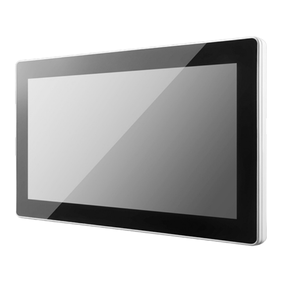
The front panel of the UTC-318 is shown in Figure 2.1. Figure 2.1 UTC-318 Front View The UTC-318 rear cover and I/O are shown in Figure 2.2. (The system features rich I/ O, including serial, Ethernet, USB, HDMI, line-out, mic-in, and DC-in ports, as well as a power button.) -
Page 17: Installation Procedures
Before you start the computer, please connect keyboard port on the I/O section of the UTC-318. 2.2.3 Switching on the Power The power switch is located at the rear of the UTC-318, as shown in Figure 2.3. Figure 2.3 Connecting the Power Cord to the DC Inlet UTC-318 User Manual... -
Page 18: Bios Setup Program Operation
UTC-318 BIOS Setup program. The setup program is stored in read-only memory (ROM) and can be accessed by resetting the system and pressing the “Del”... - Page 19 Select OS Selection [Windows 8.x/ Android / Windows7] COM2 RS232/RS422/RS485 Selection: Enter the BIOS Setup Advanced NCT6106D Super I/O Configuration UTC-318 User Manual...
- Page 20 Select Serial Port 2 Configuration Change the Serial Port 2 mode [RS232/RS422/RS485] UTC-318 User Manual...
-
Page 21: System Software Installation
2.4 System Software Installation Recent OS releases from major vendors include setup programs that automatically load and guide users through the hard disk preparation and OS installation process. The guidelines below explain the procedures for OS installation on the UTC-318 hard drive. Note! Some distributors and system integrators may pre-install software onto the UTC-318 prior to shipment. - Page 22 UTC-318 User Manual...
-
Page 23: Chapter 3 Hardware Installation And Upgrades
Chapter Hardware Installation and Upgrades This chapter explains the UTC-318 hardware installation and upgrade process. Introduction 2.5" Hard Disk Drive Installation mSATA Card Installation WLAN Installation... -
Page 24: Introduction
3.1 Introduction The UTC-318 is a touch panel computer housed in a plastic enclosure. For HDD, DRAM, or mini-SATA card installation, simply remove the rear cover. All maintenance or hardware upgrades can be easily completed upon removal of the rear cover. -
Page 25: Msata Card Installation
3.3 mSATA Card Installation Remove the 10 screws on the rear cover. Remove the 6 screws on the reinforced board. Figure 3.2 mSATA Card Installation UTC-318 User Manual... -
Page 26: Wlan Installation
However, customers can determine the specific location according to their requirements. Remove the 10 screws on the rear cover. Remove the 6 screws on the reinforced board. Coaxial cable (Advantech P/N: 1750006682-01) Connect the coaxial cable to "ANT1" on the WLAN card. UTC-318 User Manual... - Page 27 Install the WLAN card on the bottom side of the motherboard. The wireless antenna cables should be routed as shown below. UTC-318 User Manual...
- Page 28 UTC-318 User Manual...
-
Page 29: Chapter 4 Jumper Settings And Connectors
Chapter Jumper Settings and Connectors This chapter provides instruc- tions on setting jumpers and con- necting peripherals, switches, and indicators. Please read all safety precautions before beginning the installation. Jumpers and Connectors CMOS Clear for External RTC (JP3) ... -
Page 30: Jumpers And Connectors
4.1 Jumpers and Connectors 4.1.1 Setting Jumpers UTC-318 can be configured according to the application by setting jumpers. A jumper is the simplest type of electrical switch and comprises two metal pins and a small metal clip (often protected by a plastic cover) that slides over and connects the pins. -
Page 31: Jumpers And Connectors
4.1.2 Jumpers and Connectors The UTC-318 motherboard features several jumpers and connectors that enable users to configure the system according to the applications. The function of every motherboard jumper is listed in the table below. Table 4.1: Jumper and Connector Functions... -
Page 32: Jumper And Connector Locations
4.1.3 Jumper and Connector Locations Figure 4.1 Jumper and Connector Locations UTC-318 User Manual... -
Page 33: Jumpers
Pin Header 3x1P 2.54 mm 180D(M) DIP 205-1x3GS Setting Function (1-2) (2-3)* 3.3 V Table 4.4: JP3: Clear CMOS Part Number 1653004101 Footprint HD_4x1P_79_D Description Pin Header 4x1P 2.0 mm 180D(M) DIP 21N12050 Setting Function (2-3)* Normal (3-4) Clear CMOS UTC-318 User Manual... -
Page 34: Table 4.5: Jp4: At/Atx Power Sel
(1-2) (2-3)* Table 4.6: CN17: COM1 Ring Part Number 1653005101 Footprint HD_5x1P_79_D Description Pine Header 5x1P 2.0 mm 180D(M) DIP 1140-000-05SN Setting Function (1-2) Ring (3-4)* COM1 RI output +5 V (4-5)* COM1 RI output +12 V UTC-318 User Manual... - Page 35 Appendix I/O Pin Assignments...
-
Page 36: Table A.1: Cn1: Backlight
Wafer Box 8P 1.25 mm 180D(M) DIP A1251WV0-8P Pin Name +12 V_INVERTER +12 V_INVERTER BKLT_EN BRIGHT1 +12V_INVERTER Table A.2: CN3: Internal USB Part Number 1655000453 Footprint WHL5V-2M-24W1140 Description Wafer Box 2.0 mm 5P 180D(M) DIP WO/Pb JIH VEI Pin Name +5 V UTC-318 User Manual... -
Page 37: Table A.3: Cn4: Lvds
+3.3 V or +5 V LVDS0_D0- LVDS1_D0- LVDS0_D0+ LVDS1_D0+ GND- LVDS0_D1- LVDS1_D1- LVDS0_D1+ LVDS1_D1+ LVDS0_D2- LVDS1_D2- LVDS0_D2+ LVDS1_D2+- LVDS0_CLK- LVDS1_CLK- LVDS0_CLK+ LVDS1_CLK+ LVDS0_DDC_SC LVDS0_DDC_SD LVDS0_D3- LVDS1_D3- LVDS0_D3+ LVDS1_D3+ +3.3 V or +5 V +3.3 V or +5 V UTC-318 User Manual... -
Page 38: Table A.4: Cn6: Sata
Wafer Box 5P 2.5 mm 180D(M) DIP 2503-WS-5 Pin Name Table A.5: CN7: SATA Power Part Number 1659254005 Footprint SATA_7P_WATM-07DBN4A3B8UW_D Description Serial ATA 7P 1.27 mm 180D(M) DIP WATM-07DBN4A3B8 Pin Name +3.3 V +5 V +12 V UTC-318 User Manual... -
Page 39: Table A.6: Cn8: Internal Usb
Footprint WHL5V-2M-24W1140 Description Wafer Box 2.0 mm 5P 180D(M) DIP WO/Pb JIH VEI Pin Name +5 V Table A.7: CN9: Touch Part Number 1655005110 Footprint WF_5P_100_RA_D Description Wafer 5P 2.54 mm 90D(M) DIP 2542-WR-5 Pin Name SENSE UTC-318 User Manual... -
Page 40: Table A.8: Cn13: Ddr3L Sodimm
Table A.8: CN13: DDR3L SODIMM Part Number 1651002087-11 Footprint DDR3_204P_AS0A626-N2S6-7H Description DDR3 SODIMM H= 5.2 mm STD 204P SMD AS0A626-H2S6-7H Pin Name VREF_DQ UTC-318 User Manual... -
Page 41: Table A.9: Mini Pcie1: Mini Pcie
Footprint FOX_AS0B226-S68K7F Description Mini PCIe 52P 6.8 mm 90D SMD AS0B226-S68Q-7H Pin Name MPCIE1_WAKE# +3.3 VSB MPCIE_CLKREQ# CLK_MINI_PCIE- CLK_MINI_PCI+ MPCIE1_DISABLE# PLTRST# PCIE_RX- +3.3 VSB PCIE_RX+ +1.5 V SMB_CLK_MPCIE1 PCIE_TX- SMB_DAT_MPCIE1 PCIE_TX+ USB_D- USB_D+ +3.3 VSB +3.3 VSB UTC-318 User Manual... -
Page 42: Table A.10:Msata1: Msata
Table A.9: MINI PCIE1: Mini PCIe +3.3 VSB Table A.10: MSATA1: MSATA Part Number 1654002538 Footprint FOX_AS0B226-S68K7F Description Mini PCIe 52P 6.8 mm 90D SMD AS0B226-S68Q-7H Pin Name +3.3 V UTC-318 User Manual... - Page 43 Table A.10: MSATA1: MSATA SATA1_RX+ +3.3 V SATA1_RX- SATA1_TX- SATA1_TX+ +3.3 V +3.3 V +3.3 V +3.3 V UTC-318 User Manual...
-
Page 44: Table A.11:Cn16: Com2
Table A.11: CN16: COM2 Part Number 1655000197 Footprint WF_5x2P_79_BOX_D_P1R Description 1655_WF_5x2P_79_BOX_D_P1R_0.Normal Pin Name 422/485 TX- 422/485 TX+ 422 RX+ 422 RX- DSR# RTS# CTS# UTC-318 User Manual... -
Page 45: Table A.12:Cn18: Com1
Table A.12: CN18: COM1 Part Number 1655000197 Footprint WF_5x2P_79_BOX_D_P1R Description 1655_WF_5x2P_79_BOX_D_P1R_0.Normal Pin Name DTR# DSR# RTS# CTS# Table A.13: CN21: Power Switch Part Number 1655302020 Footprint WF_2P_79_BOX_R1_D Description Wafer Box 2P 2.0 mm 180D(M) DIP A2001WV2-2P Pin Name PSIN UTC-318 User Manual... -
Page 46: Table A.14:Cn22: Speakers
Part Number 1652003274 Footprint RJ45_28P_RTB-19GB9J1A Description Phone Jack RJ45 28P DIP RTB-19GB9J1A Table A.16: CN24: External USB Part Number 1654009513 Footprint USB_8P_UB1112C-8FDE-4F Description USB Conn. 8P 2.0 mm 90D DIP UB1112C-8FDE-4F Pin Name +5 VSB +5 VSB UTC-318 User Manual... -
Page 47: Table A.17:Cn25: External Usb
USB Conn. 8P 2.0 mm 90D DIP UB1112C-8FDE-4F Pin Name +5 VSB +5 VSB Table A.18: CN26: External USB Part Number 1654010199 Footprint USB_13P_UEA1112C-UHS6-4F Description USB Conn. 2.0+3.0 13P 90D(F) DIP UEA1112C-UHS6-4 Pin Name +5VSB RX_D- RX_D+ TX_D- TX_D+ +5 VSB UTC-318 User Manual... -
Page 48: Table A.19:Cn27: Line Out
Phone Jack 5P 3.5φ 90D(F) AZALIA GREEN DIP WO/P Pin Name OUT_L OUT_R Table A.20: CN28: Mic In Part Number 1652001584 Footprint KUONYI_PJ-2508PA-5-L Description Phone Jack 5P 3.5φ 90D(F) AZALIA PINK DIP WO/Pb Pin Name MIC_L MIC_R UTC-318 User Manual... -
Page 49: Table A.21:Cn30: Hdmi
Table A.21: CN30: HDMI Part Number 1654011175-01 Footprint HDMI_19P_QJ51191-LFB4-7F Description HDMI Conn. 19P 0.5 mm 90D(F) SMD QJ51191-LFB4-7F Pin Name HDMI_TX0+ HDMI_TX0- HDMI_TX1+ HDMI_TX1- HDMI_TX2+ HDMI_TX2- HDMI_TX3+ HDMI_TX3- HDMI_CLK HDMI_DAT +5 V HDMI_DET UTC-318 User Manual... -
Page 50: Table A.22:Cn31: Dc-In
Description DC Power Jack 2.5 mm 90D(M) DIP 2DC-G213B200 Pin Name DC_IN Table A.23: SW2 Button: Power Button Part Number 1600000055 Footprint SW_6P_TC003-N11AABRGXX-RK_D Description PUSH SW DIP 6P W/LED WO/Pb TC003-N11AABRGXX-RK Pin Name ATX_PWRBTN# ATX_PWRBTN# +5 V UTC-318 User Manual... - Page 51 UTC-318 User Manual...
- Page 52 No part of this publication may be reproduced in any form or by any means, including electronically, by photocopying, recording, or otherwise, without the prior written permission of the publisher. All brand and product names are trademarks or registered trademarks of their respective companies. © Advantech Co., Ltd. 2015...
Need help?
Do you have a question about the UTC-318 and is the answer not in the manual?
Questions and answers