Table of Contents

Related Manuals for Aaeon GENE-HD05


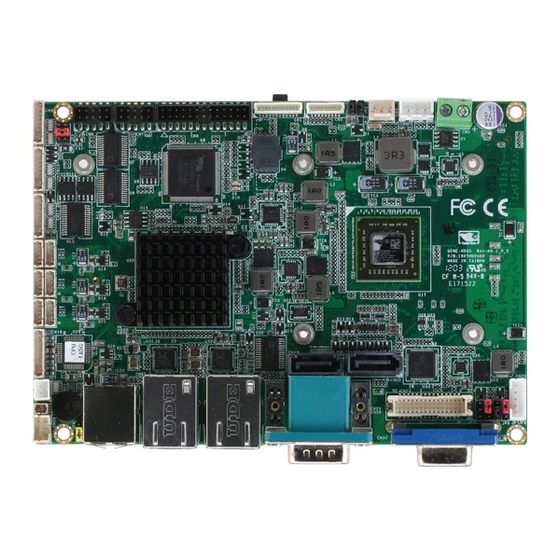
Summary of Contents for Aaeon GENE-HD05
- Page 1 GENE-HD05 3.5” Subcompact Board User‟s Manual 4 Last Updated: November 10, 2015...
-
Page 2: Copyright Notice
AAEON assumes no liabilities resulting from errors or omissions in this document, or from the use of the information contained herein. AAEON reserves the right to make changes in the product design without notice to its users. - Page 3 Acknowledgement All other products‟ name or trademarks are properties of their respective owners. ® Microsoft Windows is a registered trademark of Microsoft Corp. ® is trademark of Advanced Micro Devices. ITE is a trademark of Integrated Technology Express, Inc. ...
- Page 4 Before setting up your product, please make sure the following items have been shipped: Item Quantity GENE-HD05 Product DVD with User‟s Manual (in pdf) and drivers If any of these items are missing or damaged, please contact your distributor or sales representative immediately.
- Page 5 (if any), its specifications, dimensions, jumper/connector settings/definitions, and driver installation instructions (if any), to facilitate users in setting up their product. Users may refer to the AAEON.com for the latest version of this document. Preface...
- Page 6 Safety Precautions Please read the following safety instructions carefully. It is advised that you keep this manual for future references All cautions and warnings on the device should be noted. Make sure the power source matches the power rating of the device. Position the power cord so that people cannot step on it.
- Page 7 If any of the following situations arises, please the contact our service personnel: Damaged power cord or plug Liquid intrusion to the device iii. Exposure to moisture Device is not working as expected or in a manner as described in this manual The device is dropped or damaged Any obvious signs of damage displayed on the device...
- Page 8 FCC Statement This device complies with Part 15 FCC Rules. Operation is subject to the following two conditions: (1) this device may not cause harmful interference, and (2) this device must accept any interference received including interference that may cause undesired operation.
- Page 9 China RoHS Requirements (CN) 产品中有毒有害物质或元素名称及含量 AAEON Main Board/ Daughter Board/ Backplane 有毒有害物质或元素 部件名称 铅 汞 镉 六价铬 多溴联苯 多溴二苯醚 (Pb) (Hg) (Cd) (Cr(VI)) (PBB) (PBDE) 印刷电路板 × ○ ○ ○ ○ ○ 及其电子组件 外部信号 × ○ ○ ○ ○ ○...
- Page 10 China RoHS Requirement (EN) Poisonous or Hazardous Substances or Elements in Products AAEON Main Board/ Daughter Board/ Backplane Poisonous or Hazardous Substances or Elements Hexavalent Polybrominated Polybrominated Component Lead Mercury Cadmium Chromium Biphenyls Diphenyl Ethers (Pb) (Hg) (Cd) (Cr(VI)) (PBB) (PBDE) PCB &...
-
Page 11: Table Of Contents
Table of Contents Chapter 1 - Product Specifications ..................1 Specifications ......................2 Chapter 2 – Hardware Information ..................4 Dimensions ....................... 5 Jumpers and Connectors ..................7 List of Jumpers ......................9 2.3.1 Touch screen4/5/8-wire Selection (JP1) ........10 2.3.2 AT/ATX Power Supply Mode Selection-1 (JP2) ...... - Page 12 2.4.10 COM Port 3 Connector (CN10) ..........24 2.4.11 COM Port 4 Connector (CN11) ..........25 2.4.12 USB 2.0 Ports 7 Connector (CN12) ..........25 2.4.13 USB 2.0 Ports 8 Connector (CN13) ..........26 2.4.14 USB 2.0 Ports 5 Connector (CN14) ..........26 2.4.15 USB 2.0 Ports 6 Connector (CN15) ..........
- Page 13 Setup submenu: Main ..................45 Setup submenu: Advanced ................. 46 3.4.1 Advanced: ACPI Settings .............. 48 3.4.2 Advanced: CPU Configuration ............ 49 3.4.3 Advanced: SATA Configuration ........... 50 3.4.4 Advanced: USB Configuration ............. 51 3.4.5 Advanced: F81866 Super IO Configuration ......53 3.4.5.1 F81866 Super IO Configuration: Serial Port 1 Configuration ....................
- Page 14 Chapter 4 – Drivers Installation .................... 73 Product CD/DVD ....................74 Appendix A - Watchdog Timer Programming ..............76 Watchdog Timer Programming ................. 77 A.2 F81866 Watchdog Timer Initial Program .............. 80 Appendix B - I/O Information ....................82 I/O Address Map ....................83 First MB Memory Address Map .................
-
Page 15: Chapter 1 - Product Specifications
Chapter 1 Chapter 1 - Product Specifications... -
Page 16: Specifications
Specifications System 3.5” Form Factor ® G-series™ T56N/T40E/T40R Processor Processor SODIMM DDR3 1066/1333, up to 4GB System Memory ® A50M Chipset Fintek 8186Error! Not a valid result for table.6D I/O Chipset ® 10/100/1000Base-TX (Realtek Ethernet ... - Page 17 0 ~ 60°C (32 ~ 140°F) Operating Temperature -40 ~ 80°C (-40 ~ 176°F) Storage Temperature 0 ~ 90% Relative Humidity, Non-Condensing Operation Humidity Display ® Chipset G-series CPU integrated T56N- up to 2560 x 1600 (18W) Resolution ...
-
Page 18: Chapter 2 - Hardware Information
Chapter 2 Chapter 2 – Hardware Information... -
Page 19: Dimensions
Dimensions Component Side Component Side Component Side Chapter 2 – Hardware Information... - Page 20 Solder Side Solder Side Chapter 2 – Hardware Information...
-
Page 21: Jumpers And Connectors
Jumpers and Connectors Component Side Component Side Component Side Chapter 2 – Hardware Information... - Page 22 Solder Side Solder Side Chapter 2 – Hardware Information...
-
Page 23: List Of Jumpers
List of Jumpers Please refer to the table below for all of the board‟s jumpers that you can configure for your application Label Function Touch Screen 4/5/8-wire Mode Selection AT/ATX Power Supply Mode Selection-1 COM2 Pin8 Function Selection Clear CMOS Jumper LVDS Backlight Lightness Up/Down Selection LVDS Operating VDD Selection LVDS Backlight Lightness Control Mode Selection... -
Page 24: Touch Screen4/5/8-Wire Selection (Jp1)
2.3.1 Touch screen4/5/8-wire Selection (JP1) 4/8-wire mode 5-wire mode Function 4/8-wire (Default) 1-2 (open) 5-wire 2.3.2 AT/ATX Power Supply Mode Selection-1 (JP2) AT mode ATX mode Function AT Mode (Default) 1-2 (open) ATX Mode 2.3.3 COM2 Pin8 Function Selection (JP3) +5 V Ring (Default) +12 V... -
Page 25: Clear Cmos Selection (Jp4)
2.3.4 Clear CMOS Selection (JP4) 1 2 3 1 2 3 Normal (Default) Clear CMOS 2.3.5 LVDS Backlight Lightness Up/down Selection (JP5) 1 2 3 1 2 3 Lightness Up Lightness Down Note: Up/Down Selection is Push-Button type interface (do not use for Jumper Header) –... -
Page 26: Lvds Backlight Lightness Control Mode Selection (Jp7)
2.3.7 LVDS Backlight Lightness Control Mode Selection (JP7) 1 2 3 1 2 3 VR Mode (Default) PWM Mode 2.3.8 LVDS Backlight Inverter VCC Selection (JP8) 1 2 3 1 2 3 +12 V +5 V (Default) 2.3.9 AT/ATX Power Supply Mode Selection-2 (JP9) ATX Mode At Mode (Default) Function... -
Page 27: List Of Connectors
List of Connectors Please refer to the table below for all of the board‟s connectors that you can configure for your application Note: If CN4 (power input for 5VSB input) is not used, please short JP9 (set pin1 and pin2 to short). If CN4 (power input for 5VSB input) is used, please leave JP9 open (set pin1 and pin2 to open). - Page 28 CN17 USB 2.0 Ports 4 CN18 Audio I/O Port CN19 SATA Port1 Connector CN20 SATA Port 2 Connector CN21 +5V Output for SATA HDD CN22 LVDS Inverter / Backlight Connector CN23 LVDS Port CN24 COM Port 1 (D-SUB 9) CN25 Realtek LAN (RJ-45) Port 2 CN26 Realtek LAN (RJ-45) Port 1...
-
Page 29: Lpc Port (Cn1)
2.4.1 LPC Port (CN1) LAD0 LAD1 LAD2 LAD3 +3.3V LFRAME# LRESET# LCLK LDRQ0 LDRQ1 SERIRQ Pin Name Signal Type Signal level LAD0 +3.3V LAD1 +3.3V LAD2 +3.3V LAD3 +3.3V +3.3V +3.3V LFRAME# LRESET# +3.3V LCLK LDRQ0 LDRQ1 SERIRQ +3.3V Chapter 2 – Hardware Information... -
Page 30: Touch Screen Connector (Cn2)
2.4.2 Touch Screen Connector (CN2) 8 Wires 4 Wires TOP EXCITE BOTTOM EXCITE BOTTOM LEFT EXCITE LEFT RIGHT EXCITE RIGHT TOP SENSE BOTTOM SENSE LEFT SENSE RIGHT SENSE Pin Name Signal Type Signal Level TOP EXCITE BOTTOM EXCITE LEFT EXCITE RIGHT EXCITE TOP SENSE BOTTOM SENSE... - Page 31 8 Wires 4 Wires 5 Wires TOP EXCITE UL(Y) BOTTOM EXCITE BOTTOM UR(H) LEFT LL(L) LEFT EXCITE RIGHT RIGHT EXCITE LR(X) TOP SENSE SENSE(S) BOTTOM SENSE LEFT SENSE RIGHT SENSE Pin Name Signal Type Signal level BOTTOM LEFT RIGHT 4 Wires 5 Wires UL(Y) BOTTOM...
-
Page 32: Cpu Fan Connector (Cn3)
Pin Name Signal Type Signal level UL(Y) UR(H) LL(L) LR(X) SENSE(S) Note: Touch mode can be set by JP1 2.4.3 CPU FAN Connector (CN3) FAN_TAC FAN_POWER FAN_CTL Pin Name Signal Type Signal level FAN_POWER +12V FAN_TAC FAN_CTL Chapter 2 – Hardware Information... -
Page 33: External +5Vsb Input Connector (Cn4)
2.4.4 External +5VSB Input Connector (CN4) PS_ON# +5VSB Pin Name Signal Type Signal level PS_ON# +5VSB 2.4.5 External +5VSB Input Connector (CN5) +12V GND Pin Name Signal Type Signal level +12V +12V 2.4.6 Front Panel Connector (CN6) Chapter 2 – Hardware Information... -
Page 34: Digital Io Port Connector (Cn7)
Pin Name Signal Type Signal level PWR_BTN- PWR_BTN+ HDD_LED- HDD_LED+ SPEAKER- SPEAKER+ PWR_LED- PWR_LED+ H/W RESET- H/W RESET+ 2.4.7 Digital IO Port Connector (CN7) Pin Name Signal Type Signal level DIO0 +3.3V DIO1 +3.3V DIO2 +3.3V DIO3 +3.3V DIO4 +3.3V DIO5 +3.3V DIO6... -
Page 35: Lpt Port Connector (Cn8)
DIO7 +3.3V +3.3V +3.3V 2.4.8 LPT Port Connector (CN8) LPT Mode DIO Mode STROBE# AFD# ERROR# DIO0 PRINT# DIO1 SLIN# DIO2 DIO3 ACK# DIO7 BUSY DIO6 DIO5 SLCT DIO4 Pin Name Signal Type Signal level STROBE# AFD# ERROR# PRINT# SLIN# Chapter 2 –... -
Page 36: Com Port 2 Connector (Cn9)
ACK# BUSY SLCT 2.4.9 COM Port 2 Connector (CN9) RS-232 Pin Name Signal Type Signal level Chapter 2 – Hardware Information... - Page 37 ± 9V ± 9V ± 9V RI/+5V/+12V IN/ PWR +5V/+12V RS-422 Pin Name Signal Type Signal level RS422_TX- ± 5V RS422_RX+ RS422_TX+ ± 5V RS422_RX- NC/+5V/+12V +5V/+12V RS-485 Pin Name Signal Type Signal level RS485_D- ± 5V Chapter 2 – Hardware Information...
-
Page 38: Com Port 3 Connector (Cn10)
RS485_D+ ± 5V NC/+5V/+12V +5V/+12V Note: COM2 RS-232/422/485 can be set by BIOS setting. Default is RS-232. Pin 8 function can be set by Jumper. 2.4.10 COM Port 3 Connector (CN10) Pin Name Signal Type Signal level ± 9V ± 9V ±... -
Page 39: Com Port 4 Connector (Cn11)
2.4.11 COM Port 4 Connector (CN11) Pin Name Signal Type Signal level ± 9V ± 9V ± 9V 2.4.12 USB 2.0 Ports 7 Connector (CN12) Pin Name Signal Type Signal level +5VSB USB7_D- DIFF Chapter 2 – Hardware Information... -
Page 40: Usb 2.0 Ports 8 Connector (Cn13)
USB7_D+ DIFF 2.4.13 USB 2.0 Ports 8 Connector (CN13) Pin Name Signal Type Signal level +5VSB USB8_D- DIFF USB8_D+ DIFF 2.4.14 USB 2.0 Ports 5 Connector (CN14) Pin Name Signal Type Signal level +5VSB USB5_D- DIFF USB5_D+ DIFF Chapter 2 – Hardware Information... -
Page 41: Usb 2.0 Ports 6 Connector (Cn15)
2.4.15 USB 2.0 Ports 6 Connector (CN15) Pin Name Signal Type Signal level +5VSB USB6_D- DIFF USB6_D+ DIFF 2.4.16 USB 2.0 Ports 3 Connector (CN16) Pin Name Signal Type Signal level +5VSB USB3_D- DIFF USB3_D+ DIFF Chapter 2 – Hardware Information... -
Page 42: Usb 2.0 Ports 4 Connector (Cn17)
2.4.17 USB 2.0 Ports 4 Connector (CN17) Pin Name Signal Type Signal level +5VSB USB4_D- DIFF USB4_D+ DIFF 2.4.18 Audio I/O Port Connector (CN18) MIC_L MIC_R GND_AUDIO LINE_L_IN LINE_R_IN GND_AUDIO LEFT_OUT GND_AUDIO RIGHT_OUT +5V_AUDIO Pin Name Signal Type Signal level MIC_L MIC_R GND_AUDIO... -
Page 43: Sata Port 1 Connector (Cn19)
LEFT_OUT GND_AUDIO RIGHT_OUT +5V_AUDIO 2.4.19 SATA Port 1 Connector (CN19) Pin 1 Pin 7 Pin Name Signal Type Signal level SATA_TX+ DIFF SATA_TX- DIFF SATA_RX- DIFF SATA_RX+ DIFF 2.4.20 SATA Port 1 Connector (CN20) Pin 1 Pin 7 Pin Name Signal Type Signal level Chapter 2 –... -
Page 44: Output For Sata Hdd Connector (Cn21)
SATA_TX+ DIFF SATA_TX- DIFF SATA_RX- DIFF SATA_RX+ DIFF 2.4.21 +5V Output for SATA HDD Connector (CN21) Pin Name Signal Type Signal level 2.4.22 +5V Output for SATA HDD Connector (CN22) BLK_PWR BKL_CONTROL BKL_ENABLE Pin Name Signal Type Signal level BKL_PWR +5V / +12V BKL_CONTROL Chapter 2 –... -
Page 45: Lvds Port Connector (Cn23)
BKL_ENABLE Note: LVDS BKL_PWR can be set to +5V or +12V by JP8. LVDS BKL_CONTROL can be set by JP7. 2.4.23 LVDS Port Connector (CN23) PIN 29 PIN 30 PIN 1 PIN 2 Pin Name Signal Type Signal level BKL_ENABLE BKL_CONTROL LCD_PWR +3.3V/+5V... -
Page 46: Com Port 1 (D-Sub 9) Connector (Cn24)
LVDS_DA1+ DIFF LVDS_DA2- DIFF LVDS_DA2+ DIFF LVDS_DA3- DIFF LVDS_DA3+ DIFF DDC_DATA +3.3V DDC_CLK +3.3V LVDS_DB0- DIFF LVDS_DB0+ DIFF LVDS_DB1- DIFF LVDS_DB1+ DIFF LVDS_DB2- DIFF LVDS_DB2+ DIFF LVDS_DB3- DIFF LVDS_DB3+ DIFF LCD_PWR +3.3V/+5V LVDS_B_CLK- DIFF LVDS_B_CLK+ DIFF Note: LVDS LCD_PWR can be set to +3.3V or +5V by JP6. 2.4.24 COM Port 1 (D-SUB 9) Connector (CN24) Chapter 2 –... -
Page 47: Realtek Lan (Rj-45) Port2 Connector (Cn25)
Pin Name Signal Type Signal level ± 9V ± 9V ± 9V 2.4.25 Realtek LAN (RJ-45) Port2 Connector (CN25) ACT/LINK SPEED Pin Name Signal Type Signal level MDI0+ DIFF MDI0- DIFF MDI1+ DIFF MDI2+ DIFF MDI2- DIFF MDI1- DIFF MDI3+ DIFF MDI3- DIFF... -
Page 48: Realtek Lan (Rj-45) Port1 Connector (Cn26)
2.4.26 Realtek LAN (RJ-45) Port1 Connector (CN26) ACT/LINK SPEED Pin Name Signal Type Signal level MDI0+ DIFF MDI0- DIFF MDI1+ DIFF MDI2+ DIFF MDI2- DIFF MDI1- DIFF MDI3+ DIFF MDI3- DIFF 2.4.27 USB Port 1 and 2 Connector (CN27) Pin Name Signal Type Signal level +5VSB... -
Page 49: Hdmi Port Connector (Cn28)
+5VSB USB2_D- DIFF USB2_D+ DIFF 2.4.28 HDMI Port Connector (CN28) Pin Name Signal Type Signal level TMDS_Data2+ DIFF TMDS_ Data2- DIFF TMDS_ Data1+ DIFF TMDS_ Data1- DIFF TMDS_ Data0+ DIFF TMDS_ Data0- DIFF TMDS_Clock+ DIFF TMDS_Clock- DIFF Chapter 2 – Hardware Information... -
Page 50: Keyboard/Mouse Combo Port Connector (Cn29)
+3.3V +3.3V HPLG_DETECT 2.4.29 Keyboard/Mouse Combo Port Connector (CN29) KB_DATA KB_CLK +5VSB MS_CLK MS_DATA Pin Name Signal Type Signal level KB_ DATA KB_CLK +5VSB MS_DATA MS_CLK 2.4.30 VGA Port Connector (CN30) Chapter 2 – Hardware Information... -
Page 51: Uim Card Module Connector (Cn32)
Pin Name Signal Type Signal level GREEN BLUE RED_GND_RTN GREEN_GND_RTN BLUE_GND_RTN DDC_DATA HSYNC VSYNC DDC_CLK 2.4.31 UIM Card Module Connector (CN32) Pin Name Signal Type Signal level UIM_PWR UIM_RST Chapter 2 – Hardware Information... -
Page 52: Ddr3 Sodimm Slot (So-Dimm1)
UIM_CLK UIM_VPP UIM_DATA 2.4.32 DDR3 SODIMM Slot (SO-DIMM1) Standard Specification 2.4.33 CFast Slot (CFDA1) Pin Name Signal Type Signal level SATA_TX+ DIFF SATA_TX- DIFF SATA_RX- DIFF SATA_RX+ DIFF Chapter 2 – Hardware Information... -
Page 53: Minicard Slot (Pciea1)
PC10 PC11 PC12 PC13 +3.3V +3.3V PC14 +3.3V +3.3V PC15 PC16 PC17 2.4.34 MiniCard Slot (PCIEA1) Pin Name Signal Type Signal level PCIE_WAKE# +3.3VSB +3.3V +1.5V +1.5V PCIE_CLK_REQ# UIM_PWR UIM_DATA PCIE_REF_CLK- DIFF Chapter 2 – Hardware Information... - Page 54 UIM_CLK PCIE_REF_CLK+ DIFF UIM_RST UIM_VPP W_DISABLE# +3.3V PCIE_RST# +3.3V PCIE_RX- DIFF +3.3VSB +3.3V PCIE_RX+ DIFF +1.5V +1.5V SMB_CLK +3.3V PCIE_TX- DIFF SMB_DATA +3.3V PCIE_TX+ DIFF USB_D- DIFF Chapter 2 – Hardware Information...
- Page 55 USB_D+ DIFF +3.3VSB +3.3V +3.3VSB +3.3V +1.5V +1.5V +3.3VSB +3.3V Chapter 2 – Hardware Information...
-
Page 56: Chapter 3 - Ami Bios Setup
Chapter 3 Chapter 3 - AMI BIOS Setup... -
Page 57: System Test And Initialization
System Test and Initialization The board uses certain routines to perform testing and initialization. If an error, fatal or non-fatal, is encountered, a few short beeps or an error message will be outputted. The board can usually continue the boot up sequence with non-fatal errors. The system configuration verification routines check the current system configuration against the values stored in the CMOS memory. -
Page 58: Ami Bios Setup
AMI BIOS Setup The AMI BIOS ROM has a pre-installed Setup program that allows users to modify basic system configurations, which is stored in the battery-backed CMOS RAM and BIOS NVRAM so that the information is retained when the power is turned off. To enter BIOS Setup, press <Del>... -
Page 59: Setup Submenu: Main
Setup submenu: Main Options summary: (default setting) System Date Day MM:DD:YYYY Change the month, year and century. The „Day‟ is changed automatically. System Time HH : MM : SS Change the clock of the system. Chapter 3 – AMI BIOS Setup... -
Page 60: Setup Submenu: Advanced
Setup submenu: Advanced Options summary: (default setting) ACPI Settings System ACPI Parameters CPU Configuration CPU Configuration Parameters SATA Configuration SATA Device Options Settings USB Configuration USB Configuration Parameters F81866 Super IO Configuration System Super IO Chip Parameters Chapter 3 – AMI BIOS Setup... - Page 61 F81866 H/W Monitor Monitor hardware status Chapter 3 – AMI BIOS Setup...
-
Page 62: Advanced: Acpi Settings
3.4.1 Advanced: ACPI Settings Options summary: (default setting) ACPI Sleep State S3 (Suspend to RAM) Select the highest ACPI sleep state the system will enter when the SUSPEND button is pressed. Chapter 3 – AMI BIOS Setup... -
Page 63: Advanced: Cpu Configuration
3.4.2 Advanced: CPU Configuration Chapter 3 – AMI BIOS Setup... -
Page 64: Advanced: Sata Configuration
3.4.3 Advanced: SATA Configuration Options summary: (default setting) OnChip SATA Channel Disabled Enabled En/Disable Serial ATA OnChip SATA Type ACHI Legacy IDE Configure SATA controller operating as Legacy IDE/AHCI mode. Chapter 3 – AMI BIOS Setup... -
Page 65: Advanced: Usb Configuration
3.4.4 Advanced: USB Configuration Options summary: (default setting) Legacy USB Support Enabled Disabled Auto Enables Legacy USB Support. AUTO option disables legacy support if no USB devices are connected. DISABLE option will keep USB devices available only for EFI applications Device Name Auto (Emulation Type) - Page 66 If Auto. USB devices less than 530MB will be emulated as Floppy and remaining as Floppy and remaining as hard drive. Forced FDD option can be used to force a HDD formatted drive to boot as FDD(Ex. ZIP drive) Chapter 3 – AMI BIOS Setup...
-
Page 67: Advanced: F81866 Super Io Configuration
3.4.5 Advanced: F81866 Super IO Configuration Options summary: (default setting) Serial Port 1/2/3/4 Configuration Set Parameters of Serial Port 1/2/3/4 Parallel Port Configuration Set Parameters of Parallel Port Digital IO Port Configuration Set Input / Output of Digital IO Port Configuration Keep last state Power Failure Always on... - Page 68 Select AC power state when power is re-applied after a power failure. ERP Function Disabled Enabled ERP Function En/Disable Chapter 3 – AMI BIOS Setup...
-
Page 69: F81866 Super Io Configuration: Serial Port
3.4.5.1 F81866 Super IO Configuration: Serial Port 1 Configuration Options summary: (default setting) Serial Port Disabled Enabled En/Disable specified serial port. Change Settings Auto IO=3F8h; IRQ=4; IO=3F8h; IRQ=3,4; IO=2F8h; IRQ=3,4; Select an optimal setting for Super IO device. Chapter 3 – AMI BIOS Setup... -
Page 70: F81866 Super Io Configuration: Serial Port
3.4.5.2 F81866 Super IO Configuration: Serial Port 2 Configuration Options summary: (default setting) Serial Port Disabled Enabled En/Disable specified serial port. Change Settings Auto IO=2F8h; IRQ=3; IO=3F8h; IRQ=3,4; IO=2F8h; IRQ=3,4; Select an optimal setting for Super IO device. RS232/422,485 RS232 RS422 Chapter 3 –... - Page 71 RS485 RS232/422,485 switch Chapter 3 – AMI BIOS Setup...
-
Page 72: F81866 Super Io Configuration: Serial Port
3.4.5.3 F81866 Super IO Configuration: Serial Port 3 Configuration Options summary: (default setting) Serial Port Disabled Enabled En/Disable specified serial port. Change Settings Auto IO=3E8h; IRQ=11; IO=3E8h; IRQ=11; IO=2E8h; IRQ=11; Select an optimal setting for Super IO device. Chapter 3 – AMI BIOS Setup... -
Page 73: Configuration
3.4.5.4 F81866 Super IO Configuration: Serial Port 4 Configuration Options summary: (default setting) Serial Port Disabled Enabled En/Disable specified serial port. Change Settings Auto IO=2E8h; IRQ=11; IO=3E8h; IRQ=11; IO=2E8h; IRQ=11; Select an optimal setting for Super IO device. Chapter 3 – AMI BIOS Setup... -
Page 74: Configuration
3.4.5.5 F81866 Super IO Configuration: Parallel Port Configuration Options summary: (default setting) Parallel Port Disabled Enabled En/Disable specified parallel port. Change Settings Auto IO=378h; IRQ=5; IO=378h; IRQ=5,6,7,10,11,12; IO=278h; IRQ=5,6,7,10,11,12; IO=3BCh; IRQ=5,6,7,10,11,12; Select an optimal setting for Super IO device. Device Mode STD Printer Mode Chapter 3 –... - Page 75 SPP Mode EPP-1.9 and SPP Mode EPP-1.7 and SPP Mode ECP Mode ECP and EPP 1.9 Mode ECP and EPP 1.7 Mode Change the Printer Port mode Chapter 3 – AMI BIOS Setup...
- Page 76 3.4.5.6 F81866 Super IO Configuration: Digital IO Port Configuration Options summary: (default setting) Port 1 Input Output Set GPIO as Input or Output. Port 2 Input Output Set GPIO as Input or Output. Port 3 Input Output Set GPIO as Input or Output. Port 4 Input Chapter 3 –...
- Page 77 Output Set GPIO as Input or Output. Port 5 Input Output Set GPIO as Input or Output. Port 6 Input Output Set GPIO as Input or Output. Port 7 Input Output Set GPIO as Input or Output. Port 8 Input Output Set GPIO as Input or Output.
-
Page 78: F81866 Super Io Configuration: F81866 H/W Monitor
3.4.6 F81866 Super IO Configuration: F81866 H/W Monitor Chapter 3 – AMI BIOS Setup... -
Page 79: Setup Submenu: Chipset
Setup Submenu: Chipset Options summary: (default setting) North Bridge South Bridge Parameters South Bridge South Bridge Parameters Chapter 3 – AMI BIOS Setup... -
Page 80: Chipset: North Bridge
3.5.1 Chipset: North Bridge Options summary: (default setting) Graphics Configuration Configure Graphics Settings. Chapter 3 – AMI BIOS Setup... -
Page 81: North Bridge: Graphics Configuration
3.5.1.1 North Bridge: Graphics Configuration Options summary: (default setting) DP0 Output HDMI Disabled NB PCIE Connect Type (Display device) DP1 Output LVDS Disabled NB PCIE Connect Type (Display device) Chapter 3 – AMI BIOS Setup... -
Page 82: Chipset: South Bridge
3.5.2 Chipset: South Bridge Options summary: (default setting) Power Mode ATX Type AT Type Select power supply mode. MiniCard & msata Minicard Configuration mSATA Support MiniCard & msata Device SB HD Azalia Configuration Options for SB HD Azalia. Chapter 3 – AMI BIOS Setup... -
Page 83: South Bridge: Sb Hd Azalia Configuration
3.5.2.1 South Bridge: SB HD Azalia Configuration Options summary: (default setting) HD Audio Azalia Device Auto Disabled Enabled Enable Or Disable HD Audio Azalia Device Chapter 3 – AMI BIOS Setup... -
Page 84: Setup Submenu: Boot
Setup submenu: Boot Options summary: (default setting) Quiet Boot Disabled Enabled En/Disable showing boot logo. Launch RTL8111E PXE Disabled OpROM. Enabled En/Disable PXE boot for RTL8111E LAN Boot Option #x Set the system boot order. Hard Drive BBS Priorities Set the order of the legacy devices in this group Chapter 3 –... -
Page 85: Setup Submenu: Security
Setup submenu: Security default setting Options summary: ( Not set Administrator Password/ User Password Change User/Administrator Password You can set a User Password once an Administrator Password is set. The password will be required during boot up, or when the user enters the Setup utility. Please Note that a User Password does not provide access to many of the features in the Setup utility. -
Page 86: Setup Submenu: Save & Exit
Setup submenu: Save & Exit Options summary: (default setting) Save Changes and Reset Reset the system after saving the changes Discard Changes and Reset Reset system setup without saving any changes Restore Defaults Restore/Load Default values for all the setup options. Save as User Defaults Save the changes done so far as User Defaults Restore User Defaults... -
Page 87: Chapter 4 - Drivers Installation
Chapter 4 Chapter 4 – Drivers Installation... -
Page 88: Product Cd/Dvd
Product CD/DVD The GENE-HD05 comes with a product DVD that contains all the drivers and utilities you need to setup your product. Insert the DVD and follow the steps in the autorun program to install the drivers. In case the program does not start, follow the sequence below to install the drivers. - Page 89 Step 4 – Install AHCI Driver Please refer to Appendix D AHCI Setting Step 5 – Install Touch Driver Open the Step5 - Touch folder followed by Setup.exe Follow the instructions Drivers will be installed automatically Step 6 – Install TPM Driver Open the Step6 - TPM folder and select your OS Open the Setup.exe file in the folder Follow the instructions...
-
Page 90: Appendix A - Watchdog Timer Programming
Appendix A Appendix A - Watchdog Timer Programming... -
Page 91: Watchdog Timer Programming
A.1 Watchdog Timer Programming GENE-HD05 utilizes FINTEK 81866 chipset as its watchdog timer controller. Below are the procedures to complete its configuration and the AAEON initial watchdog timer program is also attached based on which you can develop customized program to fit your application. - Page 92 (1) Enter the MB PnP Mode To enter the MB PnP Mode, four special I/O write operations are to be performed during Wait for Key state. To ensure the initial state of the key-check logic, it is necessary to perform four write opera-tions to the Special Address port (2EH).
- Page 93 Appendix A – Watchdog Timer Programming...
-
Page 94: F81866 Watchdog Timer Initial Program
A.2 F81866 Watchdog Timer Initial Program Main(){ aaeonSuperIOOpen(); aaeonWdtSetCountMode(BOOL bMinute); // Set wdt count mode aaeonWdtSetTimeoutCount(BYTE tTimeout); // Set wdt timer aaeonWdtSetEnable(BOOL bEnable); // Enable wdt aaeonSuperIOClose(); Void aaeonSuperIOOpen(){ // Config F81866 Entry key aaeonioWritePortByte(F81866_INDEX, 0x87); aaeonioWritePortByte(F81866_INDEX, 0x87); Void aaeonWdtSetCountMode(BOOL bMinute){ BYTE WDT_CONTROL = f81866ReadByte(F81866_WDT_CONTROL_REG);... - Page 95 Void aaeonWdtSetEnable(BOOL bEnable){ f81866SetLdn(0x07); if(bEnable){ f81866WriteByte(0x30, 0x01); WDT_BASE_ADDR = (f81866ReadByte(F81866_WDT_BASEADDR_REG_MSB) << 8) | f81866ReadByte(F81866_WDT_BASEADDR_REG_LSB); WDT_STATUS = f81866ReadByte(F81866_WDT_CONTROL_REG); f81866WriteByte(F81866_WDT_CONTROL_REG, WDT_STATUS | 0x20); WDT_STATUS = f81866ReadByte(F81866_WDT_PME_REG); f81866WriteByte(F81866_WDT_PME_REG, WDT_STATUS | 0x01); }else{ f81866WriteByte(0x30, 0x00); WDT_BASE_ADDR = 0; WDT_STATUS = f81866ReadByte(F81866_WDT_CONTROL_REG); f81866WriteByte(F81866_WDT_CONTROL_REG, WDT_STATUS & 0xDF); WDT_STATUS = f81866ReadByte(F81866_WDT_PME_REG);...
-
Page 96: Appendix B - I/O Information
Appendix B Appendix B - I/O Information... -
Page 97: I/O Address Map
I/O Address Map Appendix B – I/O Information... - Page 98 Appendix B – I/O Information...
-
Page 99: First Mb Memory Address Map
First MB Memory Address Map Appendix B – I/O Information... -
Page 100: Irq Mapping Chart
IRQ Mapping Chart Appendix B – I/O Information... -
Page 101: Dma Channel Assignments
DMA Channel Assignments Appendix B – I/O Information... -
Page 102: Appendix C - Mating Connectors
Appendix C Appendix C – Mating Connectors... -
Page 103: List Of Mating Connectors And Cables
List of Mating Connectors and Cables Mating Connector Connector Available Function Cable P/N Label Cable Vendor Model no Touch Screen SHR-9V-S-B Connector CPU Fan Molex 22-01-2035 Connector External +5VSB Power Input PHR-3 ATX Cable 170220020B PS_ON# +12V Vin Power 1702002010 Connector Cable Digital I/O... - Page 104 +5Vout 2 Pins For CN21 PHR-2 1702150155 Connector HDD Power LVDS CN22 Inverter PHR-5 Connector LVDS DF13-30DS CN23 HIROSE Connector -1.25C P/S2 KB/MS P/S2 KB/MS CN29 PHDR-06VS 1700060152 Connector Cable External Battery BATA1 Molex 51021-0200 175011901C Cable Connector Appendix C – Mating Connectors...
-
Page 105: Appendix D - Ahci Settings
Appendix D Appendix D – AHCI Settings... -
Page 106: Setting Ahci
Setting AHCI OS installation to setup AHCI Mode. Step 1: Copy the files below from “Driver DVD -> STEP4 - AHCI\WinXP\SB8xx_RAID_XP_3.2.1540.92” to Disk Step 2: Connect the USB Floppy to the board (The board on the photo is just for reference) Appendix D –... - Page 107 Step 3: BIOS Setup menu select “Advanced\OnChip SATA Type -> AHCI” Step 4: Setup OS Appendix D – AHCI Settings...
- Page 108 Step 5: Press “F6” Step 6: Choose “S” Appendix D – AHCI Settings...
- Page 109 ® Step 7: Choose “AMD A50M” Step 8: It will show the model number you select and then press “ENTER” Step 9: Setup is loading files Appendix D – AHCI Settings...
-
Page 110: Appendix E - Electrical Specifications For I/O Ports
Appendix E Appendix E – Electrical Specifications for I/O Ports... -
Page 111: Electrical Specifications For Digital I/O Ports
Electrical Specifications for Digital I/O Ports Reference Signal Name Rate Output LVDS Inverter / +5V/2A or CN22 Backlight Connector +12V/2A LPC Port +3.3VCC +3.3V/0.5A CPU FAN +12V/0.5A +3.3V/(Open Digital IO Port D0~D7 drain) +5V/1A or COM Port 2 +5V/+12V +12V/0.5A USB 2.0 Ports 7 CN12 +5V/0.5A (per...
Need help?
Do you have a question about the GENE-HD05 and is the answer not in the manual?
Questions and answers