Table of Contents

Subscribe to Our Youtube Channel
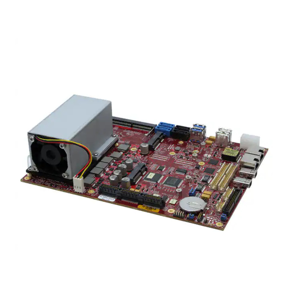
Related Manuals for VersaLogic Copperhead VL-EBX-41


Summary of Contents for VersaLogic Copperhead VL-EBX-41
-
Page 1: Reference Manual
Reference Manual DOC. REV. 7/25/2014 Copperhead (VL-EBX-41) Intel 3rd Generation Core™ ® Quad or Dual Core SBC with Ethernet, HD Graphics, ACPI 4.0, SATA, RAID, USB, eUSB, mSATA, SUMIT, HD Audio, Serial, Analog + Digital I/O, and... - Page 2 Copyright © 2014 VersaLogic Corp. All rights reserved. Notice: Although every effort has been made to ensure this document is error-free, VersaLogic makes no representations or warranties with respect to this product and specifically disclaims any implied warranties of merchantability or fitness for any particular purpose.
- Page 3 Product Release Notes Rev 1.0x – Commercial Release. Support Page The Copperhead support page, at http://www.versalogic.com/private/copperheadsupport.asp, contains additional information and resources for this product including: Reference Manual (PDF format) Operating system information and software drivers Data sheets and manufacturers’ links for chips used in this product ...
-
Page 4: Table Of Contents
Table of Contents Introduction ........................1 Description .......................... 1 Technical Specifications ..................... 2 Copperhead Block Diagram ....................3 Thermal Considerations ...................... 4 CPU Die Temperature ................... 4 Model Differences ....................4 Warnings ..........................5 Electrostatic Discharge ..................5 Lithium Battery ...................... 5 Handling Care ...................... - Page 5 Programmable LED ..................... 49 Power LED ......................50 Pushbutton Reset ......................50 Power Button ........................50 Supported Power States ..................51 Speaker ..........................51 SPX Expansion Bus ......................52 VersaLogic SPX Expansion Modules ..............52 SPI Registers ......................53 EBX-41 Reference Manual...
- Page 6 Table of Contents System Maps ........................57 On-board I/O Devices ....................... 57 Special Registers ......................58 PLED and Product Code Register ..................58 PLD Revision and Type Register ..................59 BIOS and Jumper Status Register ..................60 Appendix A – References ....................61 Appendix B –...
-
Page 7: Introduction
Introduction Description The Copperhead (VL-EBX-41) is a feature-packed single board computer designed for OEM control projects requiring fast processing, industrial I/O, flexible memory options and designed- in reliability and longevity (product lifespan). Its features include: Intel® 3rd Generation Core™ CPU: Ten USB 2.0 ports and two USB 3.0 ports ... -
Page 8: Technical Specifications
Introduction Technical Specifications Board Size: USB: EBX standard: 5.75” x 8” (146 mm x 203 mm) Ten USB 2.0 host ports Two USB 3.0 host ports Storage Temperature: Audio: -40°C to 85°C Operating Temperature: Intel HD Audio, IDT 92HD75 HD audio CODEC Stereo Line In and Stereo Line Out Standard temp. -
Page 9: Copperhead Block Diagram
Introduction Copperhead Block Diagram Figure 1. VL-EBX-41 Block Diagram EBX-41 Reference Manual... -
Page 10: Thermal Considerations
Note that Intel does not warrant their CPUs in the event of this occurrence. ODEL IFFERENCES VersaLogic offers both commercial and industrial temperature models of the VL-EBX-41. The basic operating temperature specification for Copperhead models is shown below. Thermal Solution Temp. Range... -
Page 11: Warnings
Introduction Warnings LECTROSTATIC ISCHARGE Warning! Electrostatic discharge (ESD) can damage circuit boards, disk drives and other components. The circuit board must only be handled at an ESD workstation. If an approved station is not available, some measure of protection can be provided by wearing a grounded antistatic wrist strap. -
Page 12: Technical Support
Click the link below to see all KnowledgeBase articles related to the VL-EBX-41. VersaTech KnowledgeBase If you have further questions, contact VersaLogic Technical Support at (503) 747-2261. VersaLogic support engineers are also available via e-mail at Support@VersaLogic.com. EPAIR... -
Page 13: Configuration And Setup
Inspect the system visually for any damage that may have occurred in shipping. Contact Support@VersaLogic.com immediately if any items are damaged or missing. Gather all the peripheral devices you plan to attach to the VL-EBX-41 and their interface and power cables. - Page 14 Configuration and Setup VL-PS-ATX12-300A Power Supply VL-CBR- 0401 VL-CBR- 0808 VL-EBX-41 CD-ROM Copperhead Drive SATA Hard Drive OS Installation CD-ROM VL-CBR- 0702 SATA USB Keyboard VL-CBR-1201 and Mouse (or connect LVDS to connector J32 on bottom side of board using VL-CBR-201x) Figure 2.
-
Page 15: Cmos Setup
Embedded, be sure to use Service Pack 3 (SP3) and all updates for full support of the latest hardware features. CMOS Setup See VersaLogic KnowledgeBase article VT1717 - Copperhead (VL-EBX-41 BIOS Setup Reference for complete information on CMOS Setup parameters. -
Page 16: Physical Details
Physical Details Dimensions and Mounting The VL-EBX-41 complies with all EBX standards which provide for specific mounting hole and PCIe/104 stack locations as shown in the diagram below. 7.80 7.60 0.125 DIA x8 Use 3 mm or #4 standoffs 5.80 5.70 2.80 2.65... - Page 17 Physical Details Caution The VL-EBX-41 must be supported at all eight mounting points to prevent excessive flexing when expansion modules are mated and de-mated. Flex damage caused by excessive force on an improperly mounted circuit board is not covered under the product warranty. 5.50 5.10 1.57...
- Page 18 Physical Details 2.87 0.25 0.25 2.38 0.70 1.95 0.63 0.62 0.06 0.40 Figure 5. VL-CBR-4004 Dimensions and Mounting Holes (Not to scale. All dimensions in inches.) EBX-41 Reference Manual...
- Page 19 Physical Details 56.00 3.20 30.00 11.00 3.20 2.0mm Drill 2X 33.00 44.48 8.00 89.00 M2.5 x 0.45mm PEM TSOS-M25-600 Figure 6. Heat Plate Dimensions and Mounting Holes (Not to scale. All dimensions in millimeters.) EBX-41 Reference Manual...
-
Page 20: Hardware Assembly
Physical Details ARDWARE SSEMBLY The VL-EBX-41 mounts on four hardware standoffs using the corner mounting holes (A). These standoffs are secured to the underside of the circuit board using pan head screws. Four additional standoffs (B) must be used under the circuit board to prevent excessive flexing when expansion modules are mated and separated. -
Page 21: External Connectors
Physical Details External Connectors – T VL-EBX-41 C ONNECTOR OCATIONS J26 - DisplayPort C = Pin 1 J27 - DisplayPort D J29 - User I/O J28 - SPX J22 - Ethernet LED Power J21 - DIO Ethernet 0 Ethernet 1 J19 - Analog I/O, Timers J15 J16 J15 - USB 3... -
Page 22: Vl-Ebx-41 Connector Locations - Bottom
Physical Details – B VL-EBX-41 C ONNECTOR OCATIONS OTTOM LVDS DDR3 SO-DIMM A 2 mm eUSB Flash Port Figure 9. VL-EBX-41 Connector Locations - Bottom EBX-41 Reference Manual... -
Page 23: Vl-Ebx-41 Connector Functions And Interface Cables
Physical Details VL-EBX-41 C ONNECTOR UNCTIONS AND NTERFACE ABLES The following table notes the function of each connector, as well as mating connectors and cables, and the page where a detailed pinout or further information is available. Table 1: Connector Functions and Interface Cables Connector Function Mating Connector... -
Page 24: Vl-Cbr-5013 Connector Locations
Physical Details Connector Function Mating Connector Transition Cable Description Page Cable — — DDR3 SO-DIMM A (DDR3 RAM) — — eUSB Flash Drive 2 mm eUSB flash module 1. Connectors are not installed at locations J20, J23, J30 and J31 (alternate latching Ethernet). Connectors J17, J34, and J35 are for factory use only. -
Page 25: Vl-Cbr-5013 Connector Functions
Physical Details VL-CBR-5013 C ONNECTOR UNCTIONS Table 2: VL-CBR-5013 Connector Functions Connector Function PCB Connector Description USB3, USB4 USB Type A USB Host COM0, COM1 Kycon K42-E9P/P-A4N Dual DB-9 male – Audio In/Out 3.5 mm dual audio jack High Density Connector FCI 98414-F06-50ULF 2 mm, 50-pin, keyed header COM2... -
Page 26: Jumper Blocks
Physical Details Jumper Blocks UMPERS HIPPED ONFIGURATION 2 4 6 8 1 3 5 7 Figure 12. Jumper Block Locations EBX-41 Reference Manual... -
Page 27: Jumper Summary
In – Primary system BIOS selected Out – Secondary system BIOS selected The Primary system BIOS is field upgradeable using the BIOS upgrade utility. See http://www.versalogic.com/private/Copperheadsupport.asp for more information. V6[3-4] General Purpose Input In – Causes the GPI_JMP bit in the BIOS and Jumper Status Register (BIOSJSR) at I/O port CA2h to read as ‘1’... -
Page 28: System Features
ELIVERY ONSIDERATIONS Using the VersaLogic approved power supply (VL-PS-ATX12-300A) and power cable (VL- CBR-0808) will ensure high quality power delivery to the board. Customers who design their own power delivery methods should take into consideration the guidelines below to ensure good power connections. -
Page 29: Lithium Battery
System Features Also, the specifications for typical operating current do not include any off-board power usage that may be fed through the VL-EBX-41 power connector. Expansion boards and USB devices plugged into the board will source additional power through the VL-EBX- 41 power connector. ... -
Page 30: System Ram
Voltage 1.35V Type DDR3 (VersaLogic VL-MM9 Series modules) Clearing Non-volatile RAM (NVRAM) You can clear NVRAM and reset the BIOS settings to factory defaults by following the instructions below. 1. Power off the Copperhead. 2. Install a jumper on V1[1-2]. -
Page 31: Setting The Clock
System Features ETTING THE LOCK CMOS Setup (accessed by pressing the Delete key during a system boot) can be used to set the time/date of the real-time clock. Expansion Bus /104 The PCIe/104 bus (connector J6) provides a PCIe x16 lane and two x1 lanes for add-on card expansion. - Page 32 System Features Table 6: SUMIT B Top Connector Pinout Pin Signal Name Function Pin Signal Name Function Ground Ground B_PETp0 Link B, lane 0 transmit + B_PERp0 Link B, lane 0 receive + Link B, lane 0 transmit – Link B, lane 0 receive – B_PETn0 B_PERn0 Ground...
-
Page 33: Interfaces And Connectors
25 MHz to 112 MHz. CMOS Setup provides several options for standard LVDS flat panel types. If these options do not match the requirements of the panel you are attempting to use, contact Support@VersaLogic.com for a custom video BIOS. EBX-41 Reference Manual... -
Page 34: Mini Displayport
Interfaces and Connectors Table 8: LVDS Flat Panel Display Pinout Signal Name Function Ground Not Connected LVDSA3 Diff. Data 3 (+) LVDSA3# Diff. Data 3 (-) Ground LVDSCLK0 Differential Clock (+) LVDSCLK0# Differential Clock (-) Ground LVDSA2 Diff. Data 2 (+) LVDSA2# Diff. -
Page 35: Console Redirection
Interfaces and Connectors Table 9: mini DisplayPort Connector Pinout J26, J27 J26, Signal Name J27 Pin Signal Name HOT PLUG DETECT ML_LANE0_P CONFIG 1 ML_LANE0_N CONFIG 2 ML_LANE1_P ML_LANE3_P ML_LANE1_N ML_LANE3_N ML_LANE2_P AUX_CH_P ML_LANE2_N AUX_CH_N DP_POWER ONSOLE EDIRECTION The Copperhead can be operated without using the on-board video output by redirecting the console to a serial communications port. -
Page 36: Sata Ports
Interfaces and Connectors SATA Ports The Copperhead provides two 6 GB/s SATA ports (J3 and J7) and two 3 GB/s ports (J5 and J9). All SATA connectors are standard 7-pin straight SATA friction latching connectors. The housing for the 6GB/s connectors is blue in color, and for the 3GB/s connectors it is the standard black. Power to SATA drives is supplied by the ATX power supply. - Page 37 Interfaces and Connectors Pin Signal Name Function Ground Reserved Not connected Host receiver diff. pair + +3.3V 3.3V source Host receiver diff. pair – Ground Ground +1.5V 1.5V power Ground Two Wire I/F Two wire I/F clock Host transmitter diff. pair – Two Wire I/F Two wire I/F data Host transmitter diff.
-
Page 38: Eusb
The Copperhead includes a 2 mm eUSB port at connector J36 on the bottom of the board. (Note that connector J36 does not accept 2.54 mm modules.) The VersaLogic VL-F15 Series of eUSB SSD modules are available in sizes of 2 GB or 4 GB. Contact VersaLogic Sales to order. -
Page 39: Status Led
Interfaces and Connectors Table 12: RJ45 Connector Status LEDs State Description Green/Orange Orange 1 Gbps speed (Link Speed) Green 100 Mbps speed 10 Mbps speed or cable not connected Yellow (Activity) Cable connected (intermittent with activity) Cable not connected TATUS Connector J22 provides an additional on-board Ethernet status LED interface. -
Page 40: Usb
Interfaces and Connectors The VL-EBX-41 includes ten USB 2.0 ports and two USB 3.0 ports. There are eight USB ports with standard USB Type A connectors, located on the baseboard and paddleboard. The eUSB, SUMIT, PCIe/104, and PCIe Mini Card/mSATA connectors all provide USB ports, as shown in the USB Port Map table below. -
Page 41: Serial Port Connectors
Interfaces and Connectors ERIAL ONNECTORS The pinouts of the DB9M connectors apply to the serial connectors on the VersaLogic breakout board VL-CBR-5013. These connectors use IEC 61000-4-2-rated TVS components to help protect against ESD damage. Table 15: COM0-1 Pinout – VL-CBR-5013 Connector J2... -
Page 42: Analog Input
2 (IO12) Ground 1 (GND2) Analog Input 13 5 (IO13) Analog Input 14 Analog Input 4 (IO14) Analog Input 15 (Custom*) 3 (IO15) Analog Input 16 2 (IO16) Ground 1 (GND2) Contact Sales@VersaLogic.com for information on custom orders. EBX-41 Reference Manual... -
Page 43: Analog Input Using The Spi Interface
Interfaces and Connectors SPI I NALOG NPUT SING THE NTERFACE See "SPI Registers" for a description of the SPI interface and registers. Initiating an Analog Conversion Using the SPI Interface The following procedure can be used to initiate an analog conversion using the SPI interface 1. -
Page 44: Analog Output
Analog Output 8 4 (IO24) Ground 5 (GND3) Contact Sales@VersaLogic.com for information on custom orders. Analog Output Using the SPI Interface The following procedure can be used to set an analog output using the SPI interface. 1. Set ADIOMODE = 1 for the D/A converter for channels 5-8. The D/A converter for channels 1-4 can be accessed for either setting of ADIOMODE. - Page 45 Interfaces and Connectors Write the analog output channel number (0 to 3) to Bits 3-0 and the write-and-update- channel command 3h to Bits 7-4 of SPIDATA3 (I/O address CADh) – Any write operation to this register triggers an SPI transaction. For example, if writing to the third DAC channel (channel number 2) the value written to SPIDATA3 is 32h.
-
Page 46: Digital I/O
Interfaces and Connectors Digital I/O The 40-pin I/O connector (J21) incorporates 32 digital I/O lines. Table 19 shows the function of each pin. The digital I/O lines are controlled using the SPI registers. See "SPI Registers" for a complete description of the registers. The digital lines are grouped into two banks of 16-bit bi-directional ports. -
Page 47: Digital I/O Port Configuration Using The Spi Interface
Interfaces and Connectors I/O P SPI I IGITAL ONFIGURATION SING THE NTERFACE Digital I/O channels 0-31 are accessed via SPI slave select 6 (writing 6h to the SS field in SPICONTROL). Each pair of I/O ports is configured by a set of paged I/O registers accessible through SPI. - Page 48 Interfaces and Connectors DX, CA9h AL, 30h ;SPISTATUS: 8MHz, no IRQ, left-shift DX, AL DX, CABh AL, 44h ;SPIDATA1: Mirror & Open-Drain interrupts DX, AL DX, CACh AL, 0Ah ;SPIDATA2: MCP23S17 address 0x0A DX, AL DX, CADh AL, 40h ;SPIDATA3: MCP23S17 write command DX, AL BUSY: MOV DX, CA9h...
- Page 49 Interfaces and Connectors AL, 00h ;SPIDATA1: 00h for outputs DX, AL DX, CACh AL, 00h ;SPIDATA2: MCP23S17 register address 00h DX, AL DX, CADh AL, 40h ;SPIDATA3: MCP23S17 write command DX, AL CALL BUSY ;Poll busy flag to wait for SPI transaction ;Write 55h to MCP23S17 register GPIOA DX, CABh AL, 55h...
- Page 50 Interfaces and Connectors 'D2 LSBIT_1ST = 0 SPI Shift Direction (Left Shifted) 'D1 0 = 0 This bit has no function 'D0 0 = 0 This bit has no function OUT SPICONTROL2, &H30 'INITIALIZE MCP23S17 '=================== 'MCP23S17 IOCON Register '----------------------- 'D7 BANK = 0 Registers in same bank (addresses are sequential) 'D6 MIRROR...
-
Page 51: Audio
Interfaces and Connectors WHILE (INP(SPISTATUS) AND &H1) = &H1: WEND 'DIO Input Data PRINT HEX$(INP(SPIDATA1)) WEND SYSTEM Audio The audio interface on the Copperhead is implemented using an Integrated Device Technology, Inc. 92HD87 Audio Codec. This interface is Intel High Definition Audio compatible. Drivers are available for most Windows-based and Linux operating systems. -
Page 52: Counter/Timers
An Intel WiFi Link 5300 PCI Express Mini Card (VL-WD10-CBN) is available from VersaLogic. A WiFi antenna (VL-CBR-ANT01) and a 12" WiFi card to bulkhead RP-SMA transition cable (VL-CBR-0201) are also available. For more information, contact Sales@VersaLogic.com. - Page 53 Interfaces and Connectors Table 22: PCIe Mini Card / mSATA Pinout PCIe Mini Card PCIe Mini Card mSATA mSATA Signal Name Function Signal Name Function WAKE# Wake Reserved Not connected 3.3VAUX 3.3V auxiliary source +3.3V 3.3V source Not connected Reserved Not connected Ground Ground...
-
Page 54: Pcie Mini Card Wireless Status Leds
Some PCIe modules use this signal as a second Mini Card wireless disable input. On the Copperhead, this signal is available for use for mSATA versus PCIe Mini Card detection. There is an option on the VersaLogic Features BIOS setup screen for setting the mSATA detection method. -
Page 55: User I/O Connector
Interfaces and Connectors User I/O Connector The 50-pin user I/O connector (J29) incorporates the COM ports, four USB ports, programmable LED, power LED, pushbutton reset, power button, audio line in/out, and speaker interfaces. The table below illustrates the function of each pin. Table 23: User I/O Connector Pinout CBR-5013 CBR-5013... -
Page 56: Power Led
Interfaces and Connectors To turn the LED on and off, set or clear bit D7 in I/O port CA0h. When changing the register, make sure not to alter the value of the other bits. The following code examples show how to turn the LED on and off. LED On LED Off DX,CA0H... -
Page 57: Supported Power States
Interfaces and Connectors UPPORTED OWER TATES The Copperhead supports the following power states: S0 (G0): Working. S1 (G1-S1): All processor caches are flushed, and the CPUs stop executing instructions. Power to the CPUs and RAM is maintained. Devices that do not indicate they must remain on may be powered down. -
Page 58: Spx Expansion Bus
XPANSION ODULES VersaLogic offers a number of SPX modules that provide a variety of standard functions, such as analog input, digital I/O, CANbus controller, and others. These are small boards (1.2” x 3.78”) that can mount on the PC/104 stack, using standard standoffs, or up to two feet away from the Info@VersaLogic.com... -
Page 59: Spi Registers
Interfaces and Connectors SPI R EGISTERS A set of control and data registers are available for SPI transactions. The following tables describe the SPI control registers (SPICONTROL and SPISTATUS) and data registers (SPIDATA3-0). SPICONTROL (READ/WRITE) CA8h CPOL CPHA SPILEN1 SPILEN0 MAN_SS Table 25: SPI Control Register 1 Bit Assignments Mnemonic... - Page 60 Interfaces and Connectors Mnemonic Description SPI Slave Select – These bits select which slave select will be asserted. The D2-D0 SS(2:0) SSx# pin on the baseboard will be directly controlled by these bits when MAN_SS = 1. There are two sets of definitions which depend on the state of the ADIOMODE bit in the Miscellaneous Control Register (MISCCON).
- Page 61 Interfaces and Connectors SPISTATUS (READ/WRITE) CA9h IRQSEL1 IRQSEL0 SPICLK1 SPICLK0 HW_IRQ_EN LSBIT_1ST HW_INT BUSY Table 26: SPI Control Register 2 Bit assignments Mnemonic Description IRQ Select – These bits select which IRQ will be asserted when a hardware D7-D6 IRQSEL(1:0) interrupt from a connected SPI device occurs.
- Page 62 Interfaces and Connectors SPIDATA0 (READ/WRITE) CAAh MSbit LSbit SPIDATA1 (READ/WRITE) CABh MSbit LSbit SPIDATA2 (READ/WRITE) CACh MSbit LSbit SPIDATA3 (READ/WRITE) CADh MSbit LSbit SPIDATA3 contains the most significant byte (MSB) of the SPI data word. A write to this register will initiate the SPI clock and, if the MAN_SS bit = 0, will also assert a slave select to begin an SPI bus transaction.
-
Page 63: System Maps
System Maps On-board I/O Devices Table 27: On-board I/O Devices Standard I/O Device I/O Addresses Reserved C80h-C9Bh PLD Internal 8254 Timers C9Ch-C9Fh PLED and Product ID Register CA0h Revision Indicator Register CA1h BIOS and Jumper Status Register CA2h Interrupt Control Register CA3h Interrupt Status Register CA4h... -
Page 64: Special Registers
Special Registers PLED and Product Code Register PLEDPC (Read/Write) CA0h PLED Table 28: PLEDPC Register Bit Assignments Mnemonic Description Light Emitting Diode — Controls the programmable LED on connector J29. PLED 0 = Turns LED off 1 = Turns LED on Product Code —... -
Page 65: Pld Revision And Type Register
Special Registers PLD Revision and Type Register REVTYP (Read-only) CA1h PLD4 PLD3 PLD2 PLD1 PLD0 TEMP CUSTOM BETA This register is used to indicate the PLD revision level and model of the Copperhead. Table 29: Revision and Type Register Bit Assignments Mnemonic Description PLD Code Revision Level —... -
Page 66: Bios And Jumper Status Register
Special Registers BIOS and Jumper Status Register BIOSJSR (Read/Write) CA2h BIOS_JMP BIOS_OR BIOS_SEL Reserved Reserved Reserved Reserved GPI_JMP Table 30: Special Control Register Bit Assignments Mnemonic Description System BIOS Selector Jumper Status — Indicates the status of the system BIOS_JMP BIOS selector jumper at V6[1-2]. -
Page 67: Appendix A - References
Appendix A – References Intel 3rd Generation Intel® Core™ Mobile 3rd Generation Intel® Core™ Processor Family Quad or Dual-Core Processor Datasheet Vol. Vol. Update Chipset Intel QM77 Platform Controller Hub Mobile Intel® QM77 Express Chipset (Intel® BD82QM77 PCH) Ethernet Controller Intel 82574IT Ethernet Controller Intel 8257IT Datasheet PCIe/104 Interface... -
Page 68: Appendix B - Custom Programming
Appendix B – Custom Programming PLD Interrupts The PLD can generate interrupts for the internal 8254 timers and the external SPI interrupt (which includes the DIO device interrupt). The SPI interrupt settings are discussed in the section on “SPX Expansion Bus.” This section covers the interrupt settings for the 8254 timers. NTERRUPT ONTROL EGISTER... -
Page 69: Interrupt Status Register
Special Registers NTERRUPT TATUS EGISTER This register is used for reading the status of interrupts generated by the PLD. IRQSTAT (Read-Status/Write-Clear) CA4h Reserved Reserved Reserved Reserved Reserved ISTAT_TC5 ISTAT_TC4 ISTAT_TC3 Table 32: Interrupt Status Register Bit Assignments Mnemonic Description D7-D3 Reserved These bits are reserved. -
Page 70: 8254 Timer Control Register
Special Registers 8254 Timer Control Register This register is used to set modes related to the inputs on the 8254 Timers. TIMCNTRL (Read/Write) CA5h TIM5GATE TIM4GATE TIM3GATE TM4MODE TM4SEL TM3SEL Reserved Reserved Table 33: 8254 Timer Control Register Bit Assignments Mnemonic Description TIM5GATE... - Page 71 Special Registers The 32-bit cascade mode is set in TM4MODE in the Timer Control Register. There are also internal or external clock selections for the timers in this register using the external clocks ICTC3 and ICTC4 signals on the connector at J19. The internal clock is the PCI clock divided by 8 (33.33 MHz / 8 = 4.167 MHz).
-
Page 72: Miscellaneous Control Register
Special Registers Miscellaneous Control Register This register is used to configure the control of the mSATA/PCIe Minicard slot multiplexer and for controlling the SPI access. MISCCON (Read/Write) CAEh Reserved MUXSEL2 MUXSEL1 MUXSEL0 Reserved Reserved Reserved ADIOMODE Table 34: mSATA/PCIe Mux Control Register Bit Assignments Mnemonic Description Reserved... -
Page 73: A/D And D/A Control/Status Register
Special Registers A/D and D/A Control/Status Register This register is used to control A/D and D/A conversion. ADCONSTAT (Read/Write) CAFh Reserved Reserved DACLDA1 DACLDA0 ADCBUSY1 ADCBUSY0 ADCONVST1 ADCONVST0 Table 35: A/D, D/A Control/Status Register Bit Assignments Mnemonic Description D7-D6 Reserved These bits are reserved.
Need help?
Do you have a question about the Copperhead VL-EBX-41 and is the answer not in the manual?
Questions and answers