
Related Manuals for VersaLogic Osprey


Summary of Contents for VersaLogic Osprey
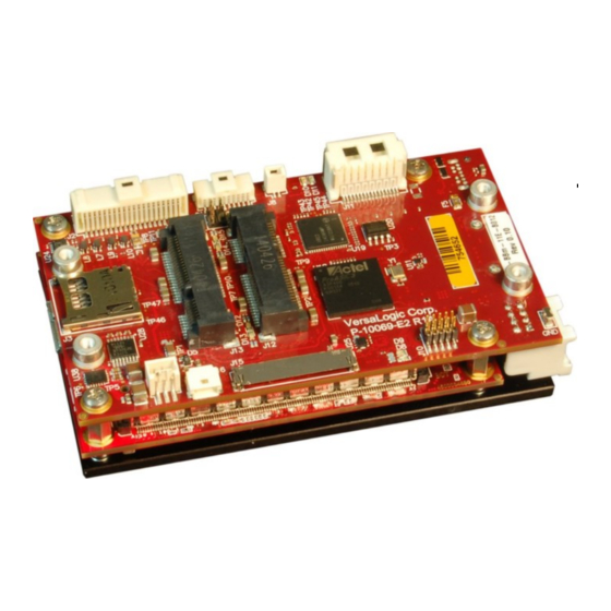
- Page 1 Programmer’s Reference Manual REV. May 2018 Osprey (VL-EPU-3311) Intel Atom™ E38xx-based ® Embedded Processing Unit with SATA, Ethernet, USB, Serial, Video, Mini PCIe Sockets, and microSD.
- Page 2 Copyright © 2016-2018 VersaLogic Corp. All rights reserved. Notice: Although every effort has been made to ensure this document is error-free, VersaLogic makes no representations or warranties with respect to this product and specifically disclaims any implied warranties of merchantability or fitness for any particular purpose.
- Page 3 Data sheets and manufacturers’ links for chips used in this product BIOS information and upgrades Utility routines and benchmark software The VersaTech KnowledgeBase is an invaluable resource for resolving technical issues with your VersaLogic product. VersaTech KnowledgeBase EPU-3311 Programmer’s Reference Manual...
-
Page 4: Table Of Contents
Contents Introduction ........................1 Related Documents ......................1 System Resources ......................2 Interrupts ..........................2 FPGA I/O Space ......................... 2 FPGA Registers ......................3 Register Access Key ......................3 Reset Status Key ......................... 3 FPGA Register Map ......................4 FPGA Register Descriptions....................7 Product Information Registers ................ - Page 5 Contents Table 17: AUXISTAT – AUX GPIO Interrupt Status Register ........15 Table 18: AUXMODE1 – AUX I/O Mode Register ............16 Table 19: WDT_CTL – Watchdog Control Register ............17 Table 20: WDT_VAL – Watchdog Control Register ............18 Table 21: XCVRMODE –...
-
Page 6: Introduction
This document is available through the software page: VersaAPI Installation and Reference Guide – describes the shared library of API calls for reading and controlling on-board devices on certain VersaLogic products. EPU-3311 Programmer’s Reference Manual... -
Page 7: System Resources
System Resources Interrupts The LPC SERIRQ is used for interrupt interface to the BayTrail SoC. Each of the following devices can have an IRQ interrupt assigned to it and each with an interrupt enable control for IRQ3, IRQ4, IRQ5, IRQ6, IRQ7, IRQ9, IRQ10, and IRQ11: ... -
Page 8: Fpga Registers
FPGA Registers This chapter describes the FPGA registers. Table 2 (beginning on the following page) lists all 64 FPGA registers Table 3 (refer to page 7) through Table 26 provide bit-level information on the individual FPGA registers Register Access Key Register Access Key Read/Write Read-only (status or reserved) -
Page 9: Fpga Register Map
FPGA Register Map Table 2: FPGA Register Map Reset Identifier Offset Address Type 1C80 Platform PLED PRODUCT_CODE 1C81 REV_LEVEL EXTEMP CUSTOM BETA 1C82 Platform LED_DEBUG WORKVER TICR 1C83 Platform IRQEN IRQSEL2 IRQSEL1 IRQSEL0 IMASK_TC5 IMASK_TC4 IMASK_TC3 TISR 1C84 Platform INTRTEST TMRTEST TMRIN4 TMRIN3... -
Page 10: Identifier
FPGA Registers Reset Identifier Offset Address Type Reserved 1C97 Reserved 1C98 Reserved 1C99 Reserved 1C9A Reserved 1C9B Reserved 1C9C Reserved 1C9D Reserved 1C9E Reserved 1C9F Reserved 1CA0 AUXDIR 1CA1 resetSX DIR_GPIO8 DIR_GPIO7 DIR_GPIO6 DIR_GPIO5 DIR_GPIO4 DIR_GPIO3 DIR_GPIO2 DIR_GPIO1 AUXPOL 1CA2 resetSX POL_GPIO8 POL_GPIO7... - Page 11 FPGA Registers Reset Identifier Offset Address Type UART1CR 1CB2 Platform IRQEN IRQSEL2 IRQSEL1 IRQSEL0 UART1_BASE3 UART1_BASE2 UART1_BASE1 UART1_BASE0 UART2CR 1CB3 Platform IRQEN IRQSEL2 IRQSEL1 IRQSEL0 UART2_BASE3 UART2_BASE2 UART2_BASE1 UART2_BASE0 Reserved 1CB4 Reserved 1CB5 UARTMODE1 1CB6 Platform UART2_485ADC UART1_485ADC UART2_EN UART1_EN UARTMODE2 1CB7 Platform...
-
Page 12: Fpga Register Descriptions
FPGA Register Descriptions Register Access Key Read/Write Read-only (status or reserved) R/WC Read-status/Write-1-to-Clear RSVD Reserved. Only write 0 to this bit; ignore all read values. RODUCT NFORMATION EGISTERS This register drives the PLED on the paddleboard. It also provides read access to the product code. -
Page 13: Bios And Jumper Status Register
FPGA Registers BIOS UMPER TATUS EGISTER Table 5: SCR –Status/Control Register Identifier Access Default Description RESERVED Reserved. Writes are ignored; reads always return 0. Debug LED (controls the yellow LED): LED_DEBUG 0 – LED is off and follows its primary function (MSATA_DAS) 1 –... -
Page 14: Table 7: Tisr - 8254 Timer Interrupt Status Register
FPGA Registers Table 7: TISR – 8254 Timer Interrupt Status Register Identifier Access Default Description RESERVED Reserved. Writes are ignored; reads always return 0. RESERVED Reserved. Writes are ignored; reads always return 0. RESERVED Reserved. Writes are ignored; reads always return 0. RESERVED Reserved. -
Page 15: Table 8: Tcr - 8254 Timer Control Register
FPGA Registers Table 8: TCR – 8254 Timer Control Register Identifier Access Default Description Debug/Test Only: Controls the “gate” signal on 8254 timer #5 when not using an external gate signal: 0 – Gate on signal GCTC5 is disabled TMR5GATE 1 –... -
Page 16: Miscellaneous Fpga Registers
FPGA Registers FPGA R ISCELLANEOUS EGISTERS MISCSR1 – Miscellaneous Control Register #1 This is a register in the always-on power well of the FPGA. It holds its state during sleep modes and can only be reset by a power cycle. This is a placeholder register for features like pushing the power-button and also for software initiated resets should those be needed. -
Page 17: Table 10: Miscsr2 - Misc. Control Register #2
FPGA Registers MISCSR2 – Miscellaneous Control Register #2 This is a register in the always-on power well of the FPGA. It holds its state during sleep modes and can only be reset by a power cycle. It is primarily used for control signals for the always-powered Ethernet controllers and the USB hubs. -
Page 18: Table 11: Miscsr3 - Misc. Control Register #3
FPGA Registers MISCSR3 – Miscellaneous Control Register #3 This register enables software to “push” the reset button. Table 11: MISCSR3 – Misc. Control Register #3 Bits Identifier Access Default Description The status of the THERMTRIP signal from the CPU module. PROCHOT 0 –... -
Page 19: Table 12: Auxdir - Aux Gpio Direction Control Register
FPGA Registers AUXDIR – AUX GPIO Direction Control Register This register controls the direction of the eight AUX GPIO signals. This reset depends on the state of the FPGA_PSEN signal. If FPGA_PSEN is a ‘0’ then the reset is the power-on and Platform Reset. If FPGA_PSEN is a ‘1’ then this register is only reset at power-on. -
Page 20: Table 15: Auxin - Aux Gpio Input Status Register
FPGA Registers AUXIN – AUX GPIO I/O Input Status Register This registers sets the AUX GPIO input value. It will read the input value regardless of the setting on the direction (that is, it always reads the input). This reads the actual state of the GPIO pin into the part. -
Page 21: Mode_Gpio8
FPGA Registers AUXMODE1– AUX I/O Mode Register #1 These two registers select the mode on each AUX GPIO. This reset depends on the state of the FPGA_PSEN signal. If FPGA_PSEN is a ‘0’ then the reset is the power-on and Platform Reset: ... -
Page 22: Wdt_En
FPGA Registers WDT_CTL – Watchdog Control Register Reset type is Platform. Table 19: WDT_CTL – Watchdog Control Register Bits Identifier Access Default Description Watchdog interrupt enable/disable: IRQEN 0 – Interrupts disabled 1 – Interrupts enabled Watchdog interrupt IRQ select in LPC SERIRQ: 000 –... -
Page 23: Com2_Mode
FPGA Registers WDT_VAL – Watchdog Value Register This register sets the number of seconds for a Watchdog prior to enabling the watchdog. By writing this value, the watchdog can be prevented from “firing”. A watchdog fires whenever this registers value is all 0s, so it must be set to a non-zero value before enabling the watchdog to prevent an immediate “firing”. -
Page 24: Table 22: Auxmode2 - Aux I/O Mode Register #2
FPGA Registers AUXMODE2– AUX I/O Mode Register #2 This register defines the interrupt mapping for the AUX GPIOs. Reset type is Platform. Table 22: AUXMODE2 - AUX I/O Mode Register #2 Bits Identifier Access Default Description AUX GPIO interrupt enable/disable: IRQEN 0 –... -
Page 25: Table 23: Uart1Cr – Uart1 Control Register (Com1)
FPGA Registers UART1CR – UART1 Control Register (COM1) Reset type is Platform. Note: The BIOS (via ACPI) may modify this register when in an ACPI-capable operating system. The register can be read for status purposes but do not write to it unless you are using a non-ACPI operating system. -
Page 26: Table 24: Uart2Cr – Uart2 Control Register (Com2)
FPGA Registers UART2CR – UART2 Control Register (COM2) Reset type is Platform. Table 24: UART2CR – UART2 Control Register (COM2) Bits Identifier Access Default Description UART interrupt enable/disable: IRQEN 0 – Interrupts disabled 1 – Interrupts enabled UART interrupt IRQ select in LPC SERIRQ: 000 –... -
Page 27: Uart2_485Adc
FPGA Registers UARTMODE1 – UART MODE REGISTER #1 When the COM Transceiver Mode is set to RS422/485 (in the XCVRMODE register) and the RS-485 Automatic Direction Control is enabled (e.g., UART1_485ADC set to ‘1’) then the transceiver Tx output is enabled. When there are bytes to transmit and the transceiver Tx output is disabled (i.e., tri-stated) when there are no bytes to transmit. -
Page 28: Fast_Mode
FPGA Registers UARTMODE2 – UART MODE REGISTER #2 Standard software (the BIOS and the operating system) assumes the baud-rate clock is 1.8432 MHz and programs the divisors accordingly; however, a faster oscillator is needed for baud rates higher than 115,200. The FAST_MODE bit in this register shifts the divisor by 4 bits (multiply by 16) so that the legacy baud rate comes out correctly for the 16x UART clock. -
Page 29: Programming Information For Hardware Interfaces
Programming Information for Hardware Interfaces Watchdog Timer A Watchdog timer is implemented within the FPGA. When triggered, the Watchdog timer can set a status bit, generate an interrupt and/or hit the push-button-reset. The Watchdog timer implements a 1-255 second timeout. The Watchdog time out is set in an 8-bit register (WDT_VAL). -
Page 30: Processor Wake# Capabilities
Programming Information for Hardware Interfaces Processor WAKE# Capabilities The following devices can wake up the processor using the PCIE_WAKE# signal to the CPU module: I210 Ethernet controller Minicard #1 WAKE# signal Minicard #2 WAKE# signal FPGA via a secondary function on one of the 8x GPIOs The following USB devices can wake up the processor using the in-band SUSPEND protocol: ...
Need help?
Do you have a question about the Osprey and is the answer not in the manual?
Questions and answers