Table of Contents
Advertisement
Quick Links
Advertisement
Table of Contents

Related Manuals for VersaLogic Viper


Summary of Contents for VersaLogic Viper
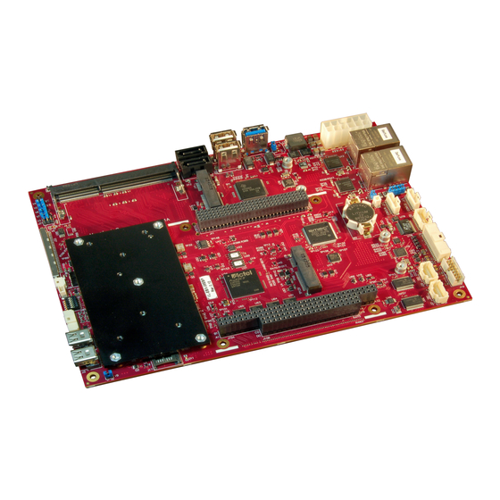
- Page 1 Programmer’s Reference Manual REV. November 2017 Viper (VL-EBX-38) Intel Atom™-based Single ® Board Computer with Dual Ethernet, Video, USB, SATA, Serial I/O, Digital I/O, Analog I/O, Trusted Platform Module security, Counter/Timers, Mini PCIe, mSATA, PC/104-Plus Interface, and SPX.
- Page 2 Copyright © 2017 VersaLogic Corp. All rights reserved. Notice: Although every effort has been made to ensure this document is error-free, VersaLogic makes no representations or warranties with respect to this product and specifically disclaims any implied warranties of merchantability or fitness for any particular purpose.
- Page 3 Utility routines and benchmark software This is a private page for EBX-38 users that can be accessed only be entering this address directly. It cannot be reached from the VersaLogic homepage. The VersaTech KnowledgeBase is an invaluable resource for resolving technical issues with your VersaLogic product.
-
Page 4: Table Of Contents
Contents Introduction ........................1 Related Documents ......................1 System Resources and Maps ..................2 Memory Map ........................2 Interrupts ..........................2 FPGA Registers ......................4 FPGA I/O Space ......................... 4 ISA Bus Addressing and LPC I/O and Memory Map ........... 4 FPGA Register Descriptions.................... - Page 5 Contents Table 12: SPI Interface Control Register ................16 Table 13: SPI Interface Status Register ................17 Table 14: SPI – SPI Debug Control Register ..............19 Table 15: MISCR1 – Misc. Control Register #1 .............. 21 Table 16: MISCSR2 – Misc. Control Register #2 ............22 Table 17: MISCR3 –...
-
Page 6: Introduction
This document is available through the software page: VersaAPI Installation and Reference Guide – describes the shared library of API calls for reading and controlling on-board devices on certain VersaLogic products. VL-EBX-38 Programmer’s Reference Manual... -
Page 7: System Resources And Maps
System Resources and Maps Memory Map Table 1: Memory Map Address Range Description 00000h – 9FFFFh Legacy system (DOS) area A0000h – B7FFFh ISA memory area (VGA frame buffer is not accessible) B8000h – BFFFFh Text mode buffer C0000h – CFFFFh Video BIOS area D0000h –... -
Page 8: Table 2: I/O Map
System Resources and Maps Per the VersaAPI standard, anytime an interrupt on the SERIRQ is enabled, the slot becomes active. All interrupts in the SERIRQ are high-true so when the slot becomes active, the slot will be low when there is no interrupt and high when there is an interrupt. Table 2: I/O Map I/O Address Range Device/Owner... -
Page 9: Fpga Registers
FPGA Registers FPGA Registers FPGA I/O Space The FPGA will be mapped into I/O space on the LPC bus. The only other devices on the LPC bus are the SCH3114 Super I/O and the TPM, but the TPM is a Memory mapped device which is not allowed to use I/O space anymore (see the main TPM section). -
Page 10: Table 4: Isa Bus I/O Map
FPGA Registers Table 4: ISA Bus I/O Map Address Range Device Size 0x2E-0x2F SCH3114 Index/Data Port 0xC00-0xC7F SCH3114 Runtime Registers 0xC80-0xCCF FPGA Registers 80 Bytes Depends on SoC LPC I/O traffic and All Other LPC I/O Cycles ISA Bus whether COM ports are enabled. Table 5: ISA Memory Map Address Range Device... -
Page 11: Fpga Register Descriptions
FPGA Registers FPGA Register Descriptions Register Access Key Read/Write Read-only (status or reserved) R/WC Read-status/Write-1-to-Clear Write-Only Read-Only and clear-to-0 after reading RSVD Reserved. Only write 0 to this bit; ignore all read values. Reset Key Power-on reset (only resets one time when input power comes on) Platform Resets prior to the processor entering the S0 power state (i.e., at power-on and in sleep states) If AUX_PSEN is a '0' in MISCSR1 (default setting) then this is the same as the Platform reset. - Page 12 FPGA Registers Identifier Address Offset Reset Platform PLED PRODUCT_CODE REV_LEVEL EXTEMP CUSTOM BETA Platform BIOS_JMP BIOS_OR BIOS_SEL LED_DEBUG WORKVER GPI_JMP TIMR Platform IRQEN IRQSEL2 IRQSEL1 IRQSEL0 IMASK_TC5 IMASK_TC4 IMASK_TC3 TISR Platform INTRTEST TMRTEST TMRIN4 TMRIN3 ISTAT_TC5 ISTAT_TC4 ISTAT_TC3 Platform TIM5GATE TIM4GATE TIM3GATE TM45MODE...
- Page 13 FPGA Registers Identifier Address Offset Reset Reserved Reserved Reserved Reserved Reserved DIOIMASK1 Platform IMASK_DIO1 DIOIMASK2 DIOISTAT1 Platform ISTAT_DIO1 DIOISTAT2 DIOCR Platform IRQEN IRQSEL2 IRQSEL1 IRQSEL0 AUXDIR resetSX DIR_GPIO8 DIR_GPIO7 DIR_GPIO6 DIR_GPIO5 DIR_GPIO4 DIR_GPIO3 DIR_GPIO2 DIR_GPIO1 AUXPOL resetSX POL_GPIO8 POL_GPIO7 POL_GPIO6 POL_GPIO5 POL_GPIO4 POL_GPIO3...
- Page 14 FPGA Registers Identifier Address Offset Reset FANTACHMS Platform <============> IMASK_BATTLO TEMPICR Platform IRQEN IRQSEL2 IRQSEL1 IRQSEL0 IMASK_EVENT IMASK_THERM IMASK_ALERT TEMPISTAT Platform BATTLOW ISTAT_BATTLOW ISTAT_EVENT ISTAT_THERM ISTAT_ALERT Reserved Reserved Reserved Reserved UARTMODE1 UARTMODE2 ISACON1 Platform ISA_IRQ11 ISA_IRQ10 ISA_IRQ9 ISA_IRQ7 ISA_IRQ6 ISA_IRQ5 ISA_IRQ4 ISA_IRQ3 ISACON2...
- Page 15 FPGA Registers Identifier Address Offset Reset UART3CR Platform UART3_EN UART3_BASE3 UART3_BASE2 UART3_BASE1 UART3_BASE0 UART4CR Platform UART4_EN UART4_BASE3 UART4_BASE2 UART4_BASE1 UART4_BASE0 Reserved Reserved Reserved Reserved Reserved Reserved Reserved Reserved Passed to ISA Bus CD0-FFFF Unknown VL-EBX-38 Programmer’s Reference Manual...
-
Page 16: Product Information Registers
FPGA Registers Product Information Registers This register drives the PLED on the paddleboard. It also provides read access to the product code. Table 6: PCR – Product Code and LED Register Identifier Access Default Description Drives the programmable LED on the paddleboard. PLED 0 –... -
Page 17: Bios And Jumper Status Register
FPGA Registers BIOS UMPER TATUS EGISTER Table 8: SCR –Status/Control Register Identifier Access Default Description Status of the external BIOS switch (jumper): BIOS_JMP 1 – Primary BIOS selected 0 – Secondary BIOS selected BIOS Switch (jumper) Override BIOS_OR 0 – BIOS Select will follow the BIOS_JMP switch setting. (Note) 1 –... -
Page 18: Timer Registers
FPGA Registers IMER EGISTERS The FPGA implements an 8254-compatible timer/counter that includes three 16-bit timers. Table 9: TICR – 8254 Timer Interrupt Mask Register Identifier Access Default Description 8254 Timer interrupt enable/disable: IRQEN 0 – Interrupts disabled 1 – Interrupts enabled 8254 Timer interrupt IRQ select in LPC SERIRQ: 000 –... -
Page 19: Table 10: Tisr - 8254 Timer Interrupt Status Register
FPGA Registers Table 10: TISR – 8254 Timer Interrupt Status Register Identifier Access Default Description Debug/Test Only -- 8254 Timer Interrupt Test (test mode only): 0 – No test interrupt: Must be set to 0 for normal operation. INTRTEST 1 – If IRQEN is a 1 then an interrupt will assert in the selected IRQ in the LPC SERIRQ stream (no timer interrupt mask needs to be set for this) Debug/Test Only -- 8254 Timer Test Mode:... -
Page 20: Table 11: Tcr - 8254 Timer Control Register
FPGA Registers Table 11: TCR – 8254 Timer Control Register Identifier Access Default Description Debug/Test Only: Controls the “gate” signal on 8254 timer #5 when not using an external gate signal: 0 – Gate on signal GCTC5 is disabled TMR5GATE 1 –... -
Page 21: Spi Control Registers
FPGA Registers SPI C ONTROL EGISTERS These are placed at the traditional offset 0x8 location. On-board SPI interface devices (DIOs, ADC, and DAC for the EBX-38) and off-board SPX interface devices use this interface. The EBX-38 is using the standard 2mm 2x7 pin header/14-pin SPX connector and can support up to four devices and an interrupt input. -
Page 22: Table 13: Spi Interface Status Register
FPGA Registers SPISTATUS The SPX interrupt is not connected on this product. The control bits and status associated are still defined in the register set but the SPX interrupt will always be de-asserted. Table 13: SPI Interface Status Register Bits Identifier Access Default... -
Page 23: Spi Data Registers
FPGA Registers SPI D EGISTERS There are four data registers used on the SPI interface. How many are used depends on the device being communicated with. SPIDATA0 is typically the least significant byte and SPIDATA3 is the most significant byte. Any write to the most significant byte SPIDATA3 initiates the SCLK and, depending on the MAN_SS state, will assert a slave select to begin an SPI bus transaction. -
Page 24: Spi Debug Control Register And Msata/Pcie Select Control Register
FPGA Registers SPI D SATA/PCI EBUG ONTROL EGISTER AND M ELECT ONTROL EGISTER This register is only used to set an SPI loopback (debug/test only) but is also used for the mSATA/PCIe Minicard Mux select. Table 14: SPI – SPI Debug Control Register Identifier Access Default... -
Page 25: Adm - A/D And D/A Spi Device Control Register
FPGA Registers ADM – A/D D/A SPI D EVICE ONTROL EGISTER This register is used to start an Analog to Digital Conversion or load a Digital to Analog value load via the SPI interface to the A/D and D/A devices. The bit positions match the similar register in the EBX-41, except there are no optional controls for a second ADC and/or DAC. -
Page 26: Miscellaneous Fpga Registers
FPGA Registers FPGA R ISCELLANEOUS EGISTERS MISCR1 – Miscellaneous Control Register #1 This is a register in the always-on power well of the FPGA. It holds its state during sleep modes and can only be reset by a power cycle. This is a placeholder register for features like pushing the power-button and also for software initiated resets should those be needed. -
Page 27: Table 16: Miscsr2 – Misc. Control Register #2
FPGA Registers Table 16: MISCSR2 – Misc. Control Register #2 Identifier Access Default Description Determines whether the hub resets only once (to support wake-up from sleep modes on USB ports) or resets every time it enters sleep modes using the platform reset: USB_HUBMODE 0 –... -
Page 28: Table 17: Miscr3 – Misc. Control Register #3
FPGA Registers MISCR3 – Miscellaneous Control Register #3 This register has miscellaneous control and status signals. The USB paddleboard power switch overcurrent status, the push-button reset signal control, and the SMBus enables for the USB Hub devices reside here. Table 17: MISCR3 – Misc. Control Register #3 Bits Identifier Access... -
Page 29: Table 18: Dioimask1 – Digital I/O 8-1 Interrupt Mask Register
FPGA Registers DIOIMASK1 – Digital I/O Interrupt Mask Register This is the interrupt mask register for the digital I/Os (the two SPI devices share a common interrupt input). Reset type is Platform. Table 18: DIOIMASK1 – Digital I/O 8-1 Interrupt Mask Register Bits Identifier Access... -
Page 30: Diocr - Digital I/O Control Register
FPGA Registers DIOCR – D I/O C IGITAL ONTROL EGISTER One interrupt can be generated for the 32 SPI based digital I/Os. Reset type is Platform Table 20: DIOCR – Digital I/O Control Register Bits Identifier Access Default Description DIO Interrupt Enable/Disable: IRQEN 0 –... -
Page 31: Table 21: Auxdir – Aux Gpio Direction Control Register
FPGA Registers AUXDIR – AUX GPIO Direction Control Register This register controls the direction of the eight AUX GPIO signals. This reset depends on the state of the AUX_PSEN signal. If AUX_PSEN is a ‘0’ then the reset is the power-on and Platform Reset. If AUX_PSEN is a ‘1’ then this register is only reset at power- Table 21: AUXDIR –... -
Page 32: Table 24: Auxin – Aux Gpio Input Status Register
FPGA Registers AUXIN – AUX GPIO I/O Input Status Register This registers sets the AUX GPIO input value. It will read the input value regardless of the setting on the direction (that is, it always reads the input). This reads the actual state of the GPIO pin into the part. -
Page 33: Table 27: Auxmode1 – Aux I/O Mode Register
FPGA Registers AUXMODE1– AUX I/O Mode Register #1 These two registers selected the mode on each AUX GPIO. This reset depends on the state of the AUX_PSEN signal. If AUX_PSEN is a ‘0’ then the reset is the power-on and Platform Reset. If AUX_PSEN is a ‘1’... -
Page 34: Table 28: Wdt_Ctl – Watchdog Control Register
FPGA Registers WDT_CTL – Watchdog Control Register Reset type is Platform. Table 28: WDT_CTL – Watchdog Control Register Bits Identifier Access Default Description Watchdog interrupt enable/disable: IRQEN 0 – Interrupts disabled 1 – Interrupts enabled Watchdog interrupt IRQ select in LPC SERIRQ: 000 –... -
Page 35: Table 29: Wdt_Val – Watchdog Control Register
FPGA Registers WDT_VAL – Watchdog Value Register This register sets the number of seconds for a Watchdog prior to enabling the watchdog. By writing this value, the watchdog can be prevented from “firing”. A watchdog fires whenever this registers value is all 0s, so it must be set to a non-zero value before enabling the watchdog to prevent an immediate “firing”. -
Page 36: Table 31: Auxmode2 - Aux I/O Mode Register #2
FPGA Registers AUXMODE2– AUX I/O Mode Register #2 This register defines the interrupt mapping for the AUX GPIOs. Reset type is Platform. Table 31: AUXMODE2 - AUX I/O Mode Register #2 Bits Identifier Access Default Description AUX GPIO interrupt enable/disable: IRQEN 0 –... -
Page 37: Table 33: Fantachls – Fantach Status Register Least Significant Bits
FPGA Registers FANTACHLS, FANTACHMS – Fan Tach Status Registers These registers contain the number of fan tach output samples over a one-second sampling period. The value is always valid after the fan speed stabilizes and is updated every 1 second (after a delay of 1 second). -
Page 38: Table 35: Tempicr – Temperature Interrupt Control Register
FPGA Registers TEMPICR – Temperature Interrupt Control Register This is the interrupt mask register for the temperature sensor thermal alerts and the DDR3L SODIMM EVENT signals and the interrupt enable and selection. The SODIMM may not have any temperature event capability. Reset type is Platform. -
Page 39: Table 36: Tempistat – Temperature Interrupt Status Register
FPGA Registers Reset type is Platform. Table 36: TEMPISTAT – Temperature Interrupt Status Register Bits Identifier Access Default Description Reads the battery low input status. IN_BATTLOW 0 – battery-low is de-asserted (battery is OK) 1 – battery-low is asserted (battery is low) Reserved Reserved. -
Page 40: Table 37: Isacon1 – Isa Control Register #1
FPGA Registers ISACONx (x = 1,2) – ISA Control Registers These register are used to enable ISA interrupts on the LPC SERIRQ. ISA interrupts simply pass through to SERIRQ and - per the ISA bus standard - are always high-true. The SERIRQEN control bit is not used for the ISA interrupt mask and should not be set until the interrupt processing is ready. -
Page 41: 8254 Timer Address 0/1/2/3 Registers
FPGA Registers Table 38: ISACON2 – ISA Control Register #2 Bits Identifier Access Default Description Status bit that is set and held when a prior LPC access was decoded to go to the ISA bus. Writes to the register bit are ignored. - Page 42 FPGA Registers UARTxCR (x = 1,2,3,4) – UART Control Registers These register are used to enable or disable the UART I/O Space for ISA bus use, and should only be used when the same changes are made for the SCH3114 register settings. The BIOS sets these according to the UART settings assigned in BIOS Setup, so do not use these unless you know what you are doing.
-
Page 43: Programming Information For Hardware Interfaces
Programming Information for Hardware Interfaces Processor WAKE# Capabilities The following devices can wake up the processor using the PCIE_WAKE# signal to the SoC: Ethernet port 0 controller Ethernet port 1 controller PCIe Minicard 0 and/or 1 (when +3.3 V power is left on during sleep modes) ... -
Page 44: Industrial I/O Functions And Spi Interface
Programming Information for Hardware Interfaces Board reset enable (when set, the board will be reset when the Watchdog timer expires). Industrial I/O Functions and SPI Interface The EBX-38 employs a set of I/O registers for controlling external serial peripheral interface (SPI) devices.
Need help?
Do you have a question about the Viper and is the answer not in the manual?
Questions and answers