
Subscribe to Our Youtube Channel
Related Manuals for VersaLogic VL-EBX-37


Summary of Contents for VersaLogic VL-EBX-37
-
Page 1: Reference Manual
Reference Manual DOC. REV. 5/25/2017 VL-EBX-37 (Mamba) Intel Core 2 Duo SBC with Video, Ethernet, USB, Serial, SATA, Audio, Analog + Digital I/O, PCIe Mini Card, eUSB, and... - Page 2 Copyright © 2014-2017 VersaLogic Corp. All rights reserved. Notice: Although every effort has been made to ensure this document is error-free, VersaLogic makes no representations or warranties with respect to this product and specifically disclaims any implied warranties of merchantability or fitness for any particular purpose.
- Page 3 VersaAPI Installation and Reference Guide This is a private page for VL-EBX-37 users that can be accessed only be entering this address directly. It cannot be reached from the public VersaLogic website. The VersaTech KnowledgeBase is an invaluable resource for resolving technical issues with your VersaLogic product.
-
Page 4: Table Of Contents
External Connectors ......................14 VL-EBX-37 Connector Locations – Top ............14 VL-EBX-37 Connector Locations – Bottom ............15 VL-EBX-37 Connector Functions and Interface Cables ........16 VL-CBR-5009 Connector Locations ..............17 VL-CBR-5009 Connector Functions ..............17 VL-CBR-4004 Connector Locations ..............18 Jumper Blocks ........................ - Page 5 Table of Contents Lithium Battery ....................21 CPU ........................... 22 System RAM ........................22 Compatible Memory Modules ................22 RAM Size Limitation ..................22 SSDDR3 Dual Function Memory and Solid State Drive ........22 CMOS RAM ........................22 Clearing CMOS RAM ..................22 CMOS Setup Defaults ......................
- Page 6 Table of Contents SPX Expansion Bus (J23) ....................49 VersaLogic SPX Expansion Modules ..............49 SPI Registers ......................50 Audio (J26) ........................53 eUSB Solid State Drive (J27) ................... 53 System Interrupts and I/O Devices ................. 54 Interrupts ........................... 54 On-board I/O Devices .......................
-
Page 7: Introduction
Customization available Thirty-two digital I/O lines The VL-EBX-37 is an EBX single board computer with an Intel Core 2 Duo processor. The board is compatible with a variety of popular operating systems including Windows, Windows Embedded, Linux, VxWorks and QNX. -
Page 8: Technical Specifications
Introduction Technical Specifications Specifications are typical at +25°C with +5V supply unless otherwise noted. Typical power is computed as the mean value of the Idle and Maximum power specifications. All power specifications represent operation at +25°C with +5V supply running Windows XP with 1 GB RAM, dual Ethernet, keyboard, and mouse. -
Page 9: Vl-Ebx-37 Block Diagram
Introduction VL-EBX-37 Block Diagram Figure 1. VL-EBX-37 Block Diagram EBX-37 Reference Manual... -
Page 10: Thermal Considerations
Note that Intel does not warrant their CPUs in the event of this occurrence. ODEL IFFERENCES VersaLogic offers both commercial and industrial temperature models of the VL-EBX-37. The basic operating temperature specification for both models is shown below. VL-EBX-37S, A: 0°C to +60°C free air, no airflow ... -
Page 11: Warnings
Note The exterior coating on some metallic antistatic bags is sufficiently conductive to cause excessive battery drain if the bag comes in contact with the bottom-side of the VL-EBX-37. ITHIUM ATTERY Warning! To prevent shorting, premature failure or damage to the lithium battery, do not place the board on a conductive surface such as metal, black conductive foam or the outside surface of a metalized ESD protective pouch. -
Page 12: Technical Support
Click the link below to see all KnowledgeBase articles related to the VL-EBX-37. VersaTech KnowledgeBase If you have further questions, contact VersaLogic Technical Support at (503) 747-2261. VersaLogic support engineers are also available via e-mail at Support@VersaLogic.com. EPAIR... -
Page 13: Configuration And Setup
Inspect the system visually for any damage that may have occurred in shipping. Contact Support@VersaLogic.com immediately if any items are damaged or missing. Gather all the peripheral devices you plan to attach to the VL-EBX-37 and their interface and power cables. - Page 14 Configuration and Setup Power VL-CBR- 0401 Supply VL-CBR- 2022 VL-EBX-37 CD-ROM Mamba SATA Drive Hard Drive OS Installation CD-ROM VL-CBR- 0701 J1/7 LVDS USB Keyboard VL-CBR-201x LVDS and Mouse Figure 2. Typical Start-up Configuration 1. Install Memory Insert DDR3 DRAM module(s) into SO-DIMM sockets J13 and J29 and latch them into place.
-
Page 15: Cmos Setup
CMOS Setup parameters. Operating System Installation The standard PC architecture used on the VL-EBX-37 makes the installation and use of most of the standard x86 processor-based operating systems very simple. The operating systems listed on VersaLogic OS Compatibility Chart use the standard installation procedures provided by the maker of the OS. -
Page 16: Physical Details
Physical Details Dimensions and Mounting The VL-EBX-37 complies with all EBX standards which provide for specific mounting hole and PC/104-Plus stack locations as shown in the diagram below. 7.80 7.60 0.125 DIA x8 Use 3 mm or #4 standoffs 5.80 5.70... - Page 17 Physical Details Caution The VL-EBX-37 must be supported at all eight mounting points to prevent excessive flexing when expansion modules are mated and de-mated. Flex damage caused by excessive force on an improperly mounted circuit board is not covered under the product warranty.
- Page 18 Physical Details 2.87 0.25 0.25 2.38 0.70 1.95 0.63 0.62 0.06 0.40 Figure 5. VL-CBR-4004 Dimensions and Mounting Holes (Not to scale. All dimensions in inches.) EBX-37 Reference Manual...
-
Page 19: Standoff Locations
ARDWARE SSEMBLY The VL-EBX-37 mounts on four hardware standoffs using the corner mounting holes (A). These standoffs are secured to the underside of the circuit board using pan head screws. Four additional standoffs (B) must be used under the circuit board to prevent excessive flexing when expansion modules are mated and separated. -
Page 20: External Connectors
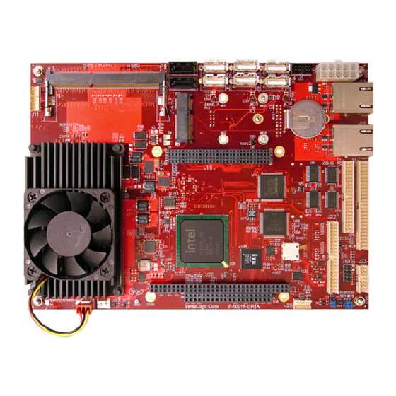
PCIe Mini Card J1, J7 SATA1, SATA0 CPU – Heatsink – Fan SO-DIMM 1 (DDR3 or = Pin 1 SSDDR3) Intel Core 2 Duo Intel GM45 (P8400) J11 – SVGA Figure 7. VL-EBX-37 Connector Locations - Top EBX-37 Reference Manual... -
Page 21: Vl-Ebx-37 Connector Locations – Bottom
VL-EBX-37 C – B ONNECTOR OCATIONS OTTOM J27 – eUSB SO-DIMM 2 (DDR3) J33 – Dual Link High Res LVDS J31 – LVDS Models A & F = Pin 1 Figure 8. VL-EBX-37 Connector Locations - Bottom EBX-37 Reference Manual... - Page 22 Physical Details VL-EBX-37 C ONNECTOR UNCTIONS AND NTERFACE ABLES The following table notes the function of each connector, as well as mating connectors and cables, and the page where a detailed pinout or further information is available. Table 1: Connector Functions and Interface Cables...
-
Page 23: Vl-Cbr-5009 Connector Functions
Physical Details VL-CBR-5009 C ONNECTOR OCATIONS Pushbutton Reset Breakout Board Adapter PS/2 Mouse (Top) Keyboard (Bottom) Speaker COM4 COM3 COM1 (Top) COM2 (Bottom) Power (Top) PLED (Bottom) Reset = Pin 1 Figure 9. VL-CBR-5009 Connectors VL-CBR-5009 C ONNECTOR UNCTIONS Table 2: VL-CBR-5009 Connector Functions Connector / Function Part Number... - Page 24 Physical Details VL-CBR-4004 C ONNECTOR OCATIONS = Pin 1 Figure 10. VL-CBR-4004 Connectors The VL-CBR-4004 can be attached to connector J7 (digital I/O) and connector J22 (analog I/O and timers). EBX-37 Reference Manual...
-
Page 25: Jumper Blocks
Physical Details Jumper Blocks UMPERS HIPPED ONFIGURATION Figure 11. Jumper Block Locations UMPER UMMARY Table 3: Jumper Summary Jumper Block Description Shipped Page [1-2] In CMOS RAM and Real-time Clock Erase [1-2] In – Normal [2-3] In – Erase CMOS RAM and real-time clock System BIOS Selector In –... -
Page 26: System Features
Power Supply (J6) OWER ONNECTOR Main power is applied to the VL-EBX-37 through an EPIC-style 10-pin polarized connector at location J6. Warning! To prevent severe and possibly irreparable damage to the system, it is critical that the power connectors are wired correctly. Make sure to use all +5V pins and all ground pins to prevent excess voltage drop. -
Page 27: Lithium Battery
ELIVERY ONSIDERATIONS The VL-EBX-37 draws 25W (5A) as measured on a typical time averaging ammeter. The board can experience large, short-term current transients during operation, so care must be taken to provide robust power to the board. A good power delivery method eliminates such problems as voltage drop and lead inductance. -
Page 28: Cpu
TATE RIVE The VersaLogic VL-MF7 Series modules provide 1 or 2 GB of RAM plus 8 GB of flash storage. These modules function only in socket J13. The solid state drive (SSD) can function as a bootable SATA drive or secondary storage device without claiming either of the SATA channels at connectors J1 or J7. -
Page 29: Cmos Setup Defaults
System Features CMOS Setup Defaults The VL-EBX-37 permits you to modify CMOS Setup defaults. This allows the system to boot up with user-defined settings from cleared or corrupted CMOS RAM, battery failure or battery-less operation. All CMOS setup defaults can be changed, except the time and date. CMOS Setup defaults can be updated with the BIOS Update Utility. -
Page 30: Primary And Backup Bios
The Super I/O chip on the VL-EBX-37 contains a hardware monitor which includes a 16-bit fan tachometer register that can be read to obtain the speed of the fan on the VL-EBX-37. When one byte of the 16-bit register is read, the other byte latches the current value until it is read, in order to ensure a valid reading. - Page 31 System Features outp( SIOINDEX, 0x07 //Point to Logical Device Config reg. outp( SIODATA, 0x0A //Select SMSC Runtime reg. outp( SIOINDEX, 0x60 //Index High Byte of Runtime reg base address. baseIOHigh = inp( SIODATA //Read High Byte. outp( SIOINDEX, 0x61 //Index Low Byte of Runtime reg base address. baseIOLow = inp( SIODATA...
-
Page 32: Interfaces And Connectors
Interfaces and Connectors SATA Ports (J1, J7) The VL-EBX-37 provides two serial ATA (SATA) ports, which communicate at a rate of up to 3.0 gigabits per second. The SATA connectors at location J1 and J7 are standard 7-pin straight SATA friction latching connectors. -
Page 33: Video Interface (J11, J31, J33)
VL-EBX-37. The controller supports dual, simultaneous, independent video output. The VL- EBX-37 can also be operated without video attached. See “Console Redirection.” The VL-EBX-37 uses a shared-memory architecture. It supports two types of video output, SVGA and LVDS Flat Panel Display. -
Page 34: Lvds Flat Panel Display Connector (J31, J33)
ONNECTOR The integrated LVDS Flat Panel Display in the VL-EBX-37 is an ANSI/TIA/EIA-644-1995 specification-compliant interface. VL-EBX-37 Models S and E have one LVDS connector at J31 and supports single-channel mode operation. Models A and F have an additional LVDS connector at J33 to provide a second channel for optional dual-channel mode (both connectors used concurrently to drive one LVDS display). -
Page 35: Compatible Lvds Panel Displays
LVDS ONSOLE EDIRECTION The VL-EBX-37 can be operated without using the on-board video output by redirecting the console to a serial communications port. CMOS Setup and some operating systems such as DOS can use this console for user interaction. Console redirection settings are configured on the Features tab of CMOS Setup. The default setting (On Remote User Detect) causes the console to be redirected to the serial port only when a signal (a Ctrl-C character) is detected from the terminal. -
Page 36: Ethernet Interface (J12, J15)
Interfaces and Connectors Ethernet Interface (J12, J15) The VL-EBX-37 features two on-board Intel 82574IT Gigabit Ethernet controllers. The controllers provide a standard IEEE 802.3 Ethernet interface for 1000Base-T, 100Base-TX, and 10Base-T applications. RJ45 connectors are located at locations J12 (Ethernet 1) and J15 (Ethernet 2). -
Page 37: Status Led (J5)
Interfaces and Connectors LED (J5) TATUS Connector J5 provides an additional on-board Ethernet status LED interface. The +3.3V power supplied to this connector is protected by a 1 Amp fuse. Table 10: Ethernet Status LED Pinout Signal Name Function +3.3V Protected Power Supply YEL1 Yellow LED - Ethernet 0... -
Page 38: Pci Express Mini Card (J14)
(VL-CBR-0201) are also available. For more information, contact Sales@VersaLogic.com. To secure a Mini Card to the VL-EBX-37 use two screws (M2 x 5 mm, Philips, pan head, 4 mm, stainless) and two washers (M2, split lock, OD 4.4 mm, stainless). Screw and washer sets are available in 10-count packages as part number VL-HDW-107. -
Page 39: Expansion Bus (J16, J20/J21)
PC/104-P – PCI (J16) PC/104-Plus modules can be secured directly to the top of the VL-EBX-37. The VL-EBX-37 is compliant with revision 2.3 of the PC/104-Plus specification and can support four bus master capable PC/104-Plus modules. The BIOS automatically allocates I/O and memory resources. -
Page 40: Digital I/O (J17)
Interfaces and Connectors Digital I/O (J17) The 40-pin I/O connector (J17) incorporates 32 digital I/O lines. Table 12 shows the function of each pin. The digital I/O lines are controlled using the SPI registers. See "SPI Registers" for a complete description of the registers. The digital lines are grouped into two banks of 16-bit bi-directional ports. -
Page 41: Digital I/O Port Configuration Using The Spi Interface
I/O pin. IRQ assignment is made in SPI control register SPISTATUS. This IRQ is shared among all SPI devices connected to the VL-EBX-37 (the ADC and DAC devices on the SPI interface do not have interrupts). Digital I/O chip interrupt configuration is achieved through I/O port register settings. - Page 42 Interfaces and Connectors DX, CA8h AL, 26h ;SPICONTROL: SPI Mode 00, 24bit, auto SPI 6 DX, AL DX, CA9h AL, 30h ;SPISTATUS: 8MHz, no IRQ, left-shift DX, AL DX, CABh AL, 44h ;SPIDATA1: Mirror & Open-Drain interrupts DX, AL DX, CACh AL, 0Ah ;SPIDATA2: MCP23S17 address 0x0A DX, AL...
- Page 43 Interfaces and Connectors ;Configure MCP23S17 register IODIRA for outputs DX, CABh AL, 00h ;SPIDATA1: 00h for outputs DX, AL DX, CACh AL, 00h ;SPIDATA2: MCP23S17 register address 00h DX, AL DX, CADh AL, 40h ;SPIDATA3: MCP23S17 write command DX, AL CALL BUSY ;Poll busy flag to wait for SPI transaction...
- Page 44 Interfaces and Connectors Reading a Digital I/O Port Using the SPI Interface The following code example reads the DIO15-DIO8 input lines. 'REGISTER ASSIGNMENT '--------------------- CONST SPICONTROL1 = &HCA8 CONST SPICONTROL2 = &HCA9 CONST SPISTATUS = &HCA9 CONST SPIDATA1 = &HCAB CONST SPIDATA2 = &HCAC CONST SPIDATA3 = &HCAD 'INITIALIZE SPI CONTROLLER...
- Page 45 Interfaces and Connectors 'D6 SLAVEFA2 " " " " 'D5 SLAVEFA1 " " " " 'D4 SLAVEFA0 " " " " 'D3 SLAVEHA2 = 0 Slave Address Bits (Hardware Address Bits) 'D2 SLAVEHA1 " " " " 'D1 SLAVEHA0 " "...
-
Page 46: Utility I/O (J18)
Interfaces and Connectors Utility I/O (J18) A number of interfaces on the VL-EBX-37 are grouped together and made accessible through utility I/O connector J18. Cables and boards are available from VersaLogic that provide discrete connectors for each of the interfaces; however, you can create custom cables that surface only the interfaces required by your application. -
Page 47: Serial Ports (J18)
Interfaces and Connectors Serial Ports (J18) The VL-EBX-37 features four on-board 16550-based serial channels located at standard PC I/O addresses. COM1 and COM2 are RS-232 (115.2 Kbps) serial ports. IRQ lines are chosen in CMOS Setup. COM ports normally cannot share interrupts with other COM ports or with other devices. -
Page 48: Serial Port Connectors
Interfaces and Connectors ERIAL ONNECTORS The pinouts of the DB-9M connectors apply to the serial connectors on the VersaLogic breakout board VL-CBR-5009. These connectors are protected against ESD damage. Table 14: COM1-2 Pinout – VL-CBR-5009 Connector J3 COM1 COM2 Top DB-9... -
Page 49: Ps/2 Keyboard And Mouse (J18)
A standard PS/2 keyboard and mouse interface is accessible through connector J4 of the VersaLogic VL-CBR-5009 breakout board. The breakout board is connected to connector J18 of the VL-EBX-37. The +5V power provided to the keyboard and mouse is protected by a 1 Amp fuse. -
Page 50: External Speaker (J18)
4 µs acquisition time, with per-channel input ranges of 0 to +5V, ±5V, 0 to +10V and ±10V. The VL-EBX-37 A/D converter is controlled using the SPI registers. The A/D converter is accessed via SPI slave select 5 (writing 5h to the SS field in SPICONTROL). -
Page 51: External Connections
Interfaces and Connectors XTERNAL ONNECTIONS Single-ended analog voltages are applied to connector J22 as shown in the following table. Standard VL-EBX-37 models include eight analog input channels. Table 17: Analog Input Pinout VL-CBR-4004 VL-CBR-4004 Signal Connector Pin (Silkscreen) Analog Input 1... - Page 52 Interfaces and Connectors 4. Write bit 0 of the analog input channel number to Bit 6, bits 2-1 of the analog input channel number to bits 5-4, and a 2-bit input range code to bits 3-2 of SPIDATA3 (I/O address CADh) – Any write operation to this register triggers an SPI transaction. The 2- bit input-range codes are 0 (±5V), 1 (±10V), 2 (0 to +5V) or 3 (0 to +10V).
-
Page 53: Analog Output (J22)
Interfaces and Connectors Analog Output (J22) The VL-EBX-37 uses a 12-bit Linear Technology LTC2634 D/A converter with four (4) single- ended output signals. The converter has 5 µs per-channel update rate with a 0 to 4.096V output voltage range. There is an expansion option to increase the output channels to eight (8). -
Page 54: Counter Timers (J22)
Interfaces and Connectors Counter Timers (J22) The VL-EBX-37 includes three uncommitted 8254 type counter/timer channels for general program use. External control signals for the three channels are available on connector J22 (see Table 19). Table 19: J22 Counter Timer Pinout... -
Page 55: Spx Expansion Bus (J23)
Interfaces and Connectors SPX Expansion Bus (J23) Up to four serial peripheral expansion (SPX) devices can be attached to the VL-EBX-37 at connector J23 using the VL-CBR-1401 or VL-CBR-1402 cable. The SPX interface provides the standard serial peripheral interface (SPI) signals: SCLK, MISO, and MOSI, as well as four chip selects, SS0# to SS3#, and an interrupt input, SINT#. -
Page 56: Spi Registers
Interfaces and Connectors SPI R EGISTERS A set of control and data registers are available for SPI transactions. The following tables describe the SPI control registers (SPICONTROL and SPISTATUS) and data registers (SPIDATA3-0). SPICONTROL (READ/WRITE) CA8h (or C98h) CPOL CPHA SPILEN1 SPILEN0 MAN_SS... - Page 57 Interfaces and Connectors SPISTATUS (READ/WRITE) CA9h (or C99h) IRQSEL1 IRQSEL0 SPICLK1 SPICLK0 HW_IRQ_EN LSBIT_1ST HW_INT BUSY Table 22: SPI Control Register 2 Bit assignments Mnemonic Description D7-D6 IRQSEL IRQ Select – These bits select which IRQ will be asserted when a hardware interrupt from a connected SPI device occurs.
- Page 58 Interfaces and Connectors SPIDATA0 (READ/WRITE) CAAh (or C9Ah) MSbit LSbit SPIDATA1 (READ/WRITE) CABh (or C9Bh) MSbit LSbit SPIDATA2 (READ/WRITE) CACh (or C9Ch) MSbit LSbit SPIDATA3 (READ/WRITE) CADh (or C9Dh) MSbit LSbit SPIDATA3 contains the most significant byte (MSB) of the SPI data word. A write to this register will initiate the SPI clock and, if the MAN_SS bit = 0, will also assert a slave select to begin an SPI bus transaction.
-
Page 59: Audio (J26)
Connector J27 on the bottom board provides an interface for an eUSB solid state drive (SSD). The VersaLogic VL-F15 series of eUSB SSDs come in a variety of sizes from 2-8 GB, as well as standard and extended temperature ratings. Contact VersaLogic Sales for information. -
Page 60: System Interrupts And I/O Devices
System Interrupts and I/O Devices Interrupts The VL-EBX-37 has the standard complement of PC-type interrupts. Up to eight IRQ lines can be allocated as needed to PCI devices. There are no interrupt configuration jumpers. All configuration is handled through CMOS Setup. -
Page 61: On-Board I/O Devices
System Resources and Maps Table 25: PCI Interrupt Settings PCI Interrupt INTA# INTB# INTC# INTD# INTE# INTF# INTG# Source 82541IT Ethernet 82574IT Ethernet SATA USB EHCI 1 USB EHCI 2 USB UHCI 1 USB UHCI 2 ... -
Page 62: Special Registers
0 = Turns LED off 1 = Turns LED on D6-D0 Product Code — These bits are hard-coded to represent the product type. The VL- EBX-37 is uniquely identified by the code 0000101. Product Code VL-EBX-37 These bits are read-only. EBX-37 Reference Manual... -
Page 63: Pld Revision And Type Register
PLD1 PLD0 TEMP CUSTOM BETA This register is used to indicate the PLD revision level and model of the VL-EBX-37. Table 28: Revision and Type Register Bit Assignments Mnemonic Description D7-D3 PLD Code Revision Level — These bits are hard-coded and represent the PLD code revision. -
Page 64: Special Control Register
Special Registers Special Control Register SCR (Read/Write) CA2h (or C92h) BIOS_JMP BIOS_OR BIOS_SEL Reserved Reserved Reserved Reserved Reserved Table 29: Special Control Register Bit Assignments Mnemonic Description BIOS_JMP System BIOS Selector Jumper Status — Indicates the status of the system BIOS selector jumper at V2[1-2]. -
Page 65: Appendix A - References
Appendix A – References Intel Core 2 Duo Intel Core 2 Duo Datasheet Chipset Intel GM45 Intel GM45 Datasheet Intel ICH9 Intel ICH9 Datasheet Super I/O Chip SMSC SCH3114 SCH3114 Datasheet Ethernet Controller Intel 82574IT Ethernet Controller Intel 8257IT Datasheet PC/104 Interface PC/104 Specification PC/104-Plus Interface... -
Page 66: Appendix B - Custom Programming
Appendix B – Custom Programming PLD Interrupts The PLD can generate interrupts for the internal 8254 timers and the external SPI interrupt (which includes the DIO device interrupt). The SPI interrupt settings are discussed in the section on “SPX Expansion Bus (J23).” This section covers the interrupt settings for the 8254 timers. NTERRUPT ONTROL EGISTER... -
Page 67: Interrupt Status Register
Special Registers NTERRUPT TATUS EGISTER This register is used for reading the status of interrupts generated by the PLD. IRQSTAT (Read-Status/Write-Clear) CA4h (or C94h) Reserved Reserved Reserved Reserved Reserved ISTAT_TC5 ISTAT_TC4 ISTAT_TC3 Table 31: Interrupt Status Register Bit Assignments Mnemonic Description D7-D3 Reserved... -
Page 68: 8254 Timer Control Register
Special Registers 8254 Timer Control Register This register is used to set modes related to the inputs on the 8254 Timers. TIMCNTRL (Read/Write) CA5h (or C95h) TIM5GATE TIM4GATE TIM3GATE TM4MODE TM4SEL TM3SEL Reserved Reserved Table 32: 8254 Timer Control Register Bit Assignments Mnemonic Description Sets the level on the Gate input for the 8254 Timer #5. - Page 69 Special Registers The 32-bit cascade mode is set in TM4MODE in the Timer Control Register. There are also internal or external clock selections for the timers in this register using the external clocks ICTC3 and ICTC4 signals on the connector at J22. The internal clock is the PCI clock divided by 8 (33.33 MHz / 8 = 4.167 MHz).
-
Page 70: 8254 Timer Base Address
Special Registers 8254 Timer Base Address This register is used to set the I/O base address on the 8254 Timers. The timers only require 4 continuous bytes of I/O memory space (byte addressing only). The address must be 8-byte aligned. Two 8-bit registers must be set. Make sure there is a space opened up in the LPC space for this base address. -
Page 71: A/D And D/A Control/Status Register
Special Registers A/D and D/A Control/Status Register This register is used to control A/D and D/A conversion. ADCONSTAT (Read/Write) CAFh (or C9Fh) Reserved Reserved Reserved DACLDA0 Reserved ADCBUSY0 Reserved ADCONVST0 Table 35: A/D, D/A Control/Status Register Bit Assignments Mnemonic Description D7-D6 Reserved These bits are reserved.
Need help?
Do you have a question about the VL-EBX-37 and is the answer not in the manual?
Questions and answers