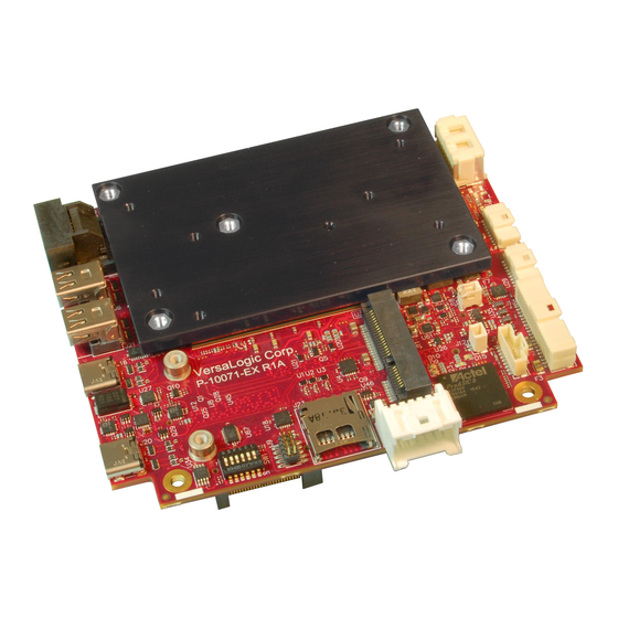
VersaLogic Lion VL-EPMe-42 Reference Manual
Intel core-based single board computer with dual ethernet, video, usb, sata, serial i/o, digital i/o, trusted platform module security, counter/timers, mini pcie, msata, spx, and pcie/104 onebank interface
Hide thumbs
Also See for Lion VL-EPMe-42:
- Hardware reference manual (56 pages) ,
- Bios reference manual (77 pages)
Table of Contents
Advertisement
Quick Links
Advertisement
Table of Contents

Related Manuals for VersaLogic Lion VL-EPMe-42


Summary of Contents for VersaLogic Lion VL-EPMe-42
- Page 1 Programmer’s Reference Manual REV. May 2018 Lion (VL-EPMe-42) Intel Core™-based Single Board Computer with ® Dual Ethernet, Video, USB, SATA, Serial I/O, Digital I/O, Trusted Platform Module security, Counter/Timers, Mini PCIe, mSATA, SPX, and PCIe/104™ OneBank™ Interface...
- Page 2 Copyright © 2017-2018 VersaLogic Corp. All rights reserved. Notice: Although every effort has been made to ensure this document is error-free, VersaLogic makes no representations or warranties with respect to this product and specifically disclaims any implied warranties of merchantability or fitness for any particular purpose.
- Page 3 Data sheets and manufacturers’ links for chips used in this product BIOS information and upgrades Utility routines and benchmark software The VersaTech KnowledgeBase is an invaluable resource for resolving technical issues with your VersaLogic product. VersaTech KnowledgeBase Lion (VL-EPMe-42) Programmer’s Reference Manual...
-
Page 4: Table Of Contents
Contents Overview ........................1 Related Documents ......................1 System Resources and Maps ..................2 Memory Map ........................2 Interrupts ..........................2 FPGA Registers ......................4 FPGA I/O Space ......................... 4 FPGA Register Map ......................5 FPGA Register Descriptions....................8 Product Information Registers ................8 BIOS and Jumper Status Register ................ -
Page 5: Overview
BIOS Setup utility. All BIOS menus, submenus, and configuration options are described. This document is available through the software page: VersaAPI Installation and Reference Guide – describes the shared library of API calls for reading and controlling on-board devices on certain VersaLogic products. Lion (VL-EPMe-42) Programmer’s Reference Manual... -
Page 6: System Resources And Maps
System Resources and Maps Memory Map Table 1: Memory Map Address Range Description 00000h – 9FFFFh Legacy system (DOS) area A0000h – B7FFFh ISA memory area (VGA frame buffer is not accessible) B8000h – BFFFFh Text mode buffer C0000h – CFFFFh Video BIOS area D0000h –... - Page 7 System Resources and Maps Table 2: I/O Map I/O Address Range Device/Owner 2F8h – 2FFh COM2 serial port default 3B0h – 3DFh Legacy VGA registers 3F8h – 3FFh COM1 serial port default 400h – 47Fh ACPI / Power management (reserved) 500h –...
-
Page 8: Fpga Registers
FPGA Registers FPGA Registers FPGA I/O Space The FPGA is mapped into I/O space on the LPC bus. The address range is mapped into 64 byte I/O window. FPGA access: LPC I/O space FPGA access size: All 8-bit byte accesses (16-bit like registers are aligned on 16-bit word boundaries to make word access possible in software but the LPC bus still splits the accesses into two 8-bit accesses) ... -
Page 9: Fpga Register Map
FPGA Registers FPGA Register Map Register Access Key Reset Status Key Read/Write Power-on reset (only resets one time when input power comes on) Resets prior to the processor entering the S0 power state (that is, at power-on Read-only (status or reserved) Platform and in sleep states) •... - Page 10 FPGA Registers Platform <============> SPIDATA2 Platform <============> SPIDATA3 Most Significant Byte and Start SPI Cycle when written Platform MUXSEL2 MUXSEL1 MUXSEL0 SERIRQEN SPILB SPIMISC - Custom SPI I/F controls, mSATA/PCIe Mux Select Reserved AUX_PSEN MINI_PSDIS MISCSR1 - Power Control Regs W_DISABLE ETH1_OFF ETH0_OFF...
- Page 11 FPGA Registers resetSX MODE_GPIO8 MODE_GPIO7 MODE_GPIO6 MODE_GPIO5 MODE_GPIO4 MODE_GPIO3 MODE_GPIO2 MODE_GPIO1 AUXMODE1 - AUX GPIO I/O Mode Register Platform IRQEN IRQSEL2 IRQSEL1 IRQSEL0 RESET_EN WDT_EN WDT_STAT WDT_CTL - Watchdog Control Platform <============> WDT_VAL - Watchdog Value (in seconds) Platform COM2_MODE COM1_MODE XCVRMODE - COM Port Transceiver Mode Register (all ports) Platform...
-
Page 12: Fpga Register Descriptions
FPGA Registers FPGA Register Descriptions Register Access Key Read/Write Read-only (status or reserved) R/WC Read-status/Write-1-to-Clear RSVD Reserved. Only write 0 to this bit; ignore all read values. Product Information Registers This register drives the PLED on the paddleboard. It also provides read access to the product code. Table 4: PCR –... -
Page 13: Bios And Jumper Status Register
FPGA Registers BIOS and Jumper Status Register Table 6: SCR –Status/Control Register Identifier Access Default Description Status of the external BIOS switch (jumper): BIOS_JMP 1 – Primary BIOS selected 0 – Secondary BIOS selected BIOS Switch (jumper) Override 0 – BIOS Select will follow the BIOS_JMP switch setting. (Note) BIOS_OR 1 –... - Page 14 FPGA Registers Table 7: BIOS Selection BIOS_OR BIOS_SEL BIOS BIOS Selected Comments (Bit 6) Configuration (Bit 5) Switch #6 Position ‘0’ ‘X’ (don’t care) “OFF” Primary Configuration Switch selects the BIOS (BIOS_SEL ignored) ‘0’ ‘X’ (don’t care) “ON” Secondary Configuration Switch selects the BIOS (BIOS_SEL ignored) ‘1’...
-
Page 15: Timer Registers
FPGA Registers Timer Registers The FPGA implements an 8254-compatible timer/counter that includes three 16-bit timers. Table 8: TICR – 8254 Timer Interrupt Control Register Identifier Access Default Description 8254 Timer interrupt enable/disable: IRQEN 0 – Interrupts disabled 1 – Interrupts enabled 8254 Timer interrupt IRQ select in LPC SERIRQ: 000 –... - Page 16 FPGA Registers Table 9: TISR – 8254 Timer Interrupt Status Register Identifier Access Default Description Debug/Test Only -- 8254 Timer Interrupt Test (test mode only): 0 – No test interrupt 1 – If IRQEN is a 1 then an interrupt will assert in the selected INTRTEST IRQ in the LPC SERIRQ stream (no timer interrupt mask needs to be set for this)
- Page 17 FPGA Registers Table 10: TCR – 8254 Timer Control Register Identifier Access Default Description Controls the “gate” signal on 8254 timer #5 when not using an external gate signal: 0 – Gate on signal GCTC5 is disabled TMR5GATE 1 – Gate on signal GCTC5 is enabled Always set to 0 when configuring timer modes.
-
Page 18: Spi Control Registers
FPGA Registers SPI Control Registers These are placed at the traditional offset 0x8 location. Only external SPX interface devices use this interface. Because the board uses a 9-pin SPX connector, only two devices are supported. SPICONTROL Table 11: SPI Interface Control Register Identifier Access Default... - Page 19 FPGA Registers SPISTATUS The SPX interrupt is not connected on this product. The control bits and status associated are still defined in the register set but the SPX interrupt will always be de-asserted. Table 12: SPI Interface Status Register Bits Identifier A c c e s s D e f a u l t...
-
Page 20: Spi Data Registers
FPGA Registers SPI Data Registers There are four data registers used on the SPI interface. How many are used depends on the device being communicated with. SPIDATA0 is typically the least significant byte and SPIDATA3 is the most significant byte. Any write to the most significant byte SPIDATA3 initiates the SCLK and, depending on the MAN_SS state, will assert a slave select to begin an SPI bus transaction. -
Page 21: Spi Debug Control Register And Msata/Pcie Select Control Register
FPGA Registers SPI Debug Control Register and mSATA/PCIe Select Control Register This register is only used to set an SPI loopback (debug/test only) but is also used for the mSATA/PCIe Minicard Mux select. Table 13: SPI – SPI Debug Control Register Identifier Access Default... -
Page 22: Miscellaneous Fpga Registers
FPGA Registers Miscellaneous FPGA Registers MISCR1 – Miscellaneous Control Register #1 This is a register in the always-on power well of the FPGA. It holds its state during sleep modes and can only be reset by a power cycle. This is a placeholder register for features like pushing the power-button and also for software initiated resets should those be needed. - Page 23 FPGA Registers Table 15: MISCSR2 – Misc. Control Register #2 Identifier Access Default Description RESERVED 0’s Reserved – Writes are ignored. Reads always return 0 Used to control the W_DISABLE (Wireless Disable) signal going to the PCIe Mincard: 0 – W_DISABLE signal is not asserted (Enabled) W_DISABLE 1 –...
- Page 24 FPGA Registers AUXDIR – AUX GPIO Direction Control Register This register controls the direction of the eight AUX GPIO signals. This reset depends on the state of the FPGA_PSEN signal. If FPGA_PSEN is a ‘0’ then the reset is the power-on and Platform Reset.
- Page 25 FPGA Registers AUXIN – AUX GPIO I/O Input Status Register This registers sets the AUX GPIO input value. It will read the input value regardless of the setting on the direction (that is, it always reads the input). This reads the actual state of the GPIO pin into the part. Table 20: AUXIN –...
- Page 26 FPGA Registers AUXMODE1– AUX I/O Mode Register #1 These two registers selected the mode on each AUX GPIO. This reset depends on the state of the FPGA_PSEN signal. If FPGA_PSEN is a ‘0’ then the reset is the power-on and Platform Reset. If FPGA_PSEN is a ‘1’...
- Page 27 FPGA Registers WDT_CTL – Watchdog Control Register Reset type is Platform. Table 24: WDT_CTL – Watchdog Control Register Bits Identifier Access Default Description Watchdog interrupt enable/disable: IRQEN 0 – Interrupts disabled 1 – Interrupts enabled Watchdog interrupt IRQ select in LPC SERIRQ: 000 –...
- Page 28 FPGA Registers WDT_VAL – Watchdog Value Register This register sets the number of seconds for a Watchdog prior to enabling the watchdog. By writing this value, the watchdog can be prevented from “firing”. A watchdog fires whenever this registers value is all 0s, so it must be set to a non-zero value before enabling the watchdog to prevent an immediate “firing”.
- Page 29 FPGA Registers AUXMODE2– AUX I/O Mode Register #2 This register defines the interrupt mapping for the AUX GPIOs. Reset type is Platform. Table 27: AUXMODE2 - AUX I/O Mode Register #2 Bits Identifier Access Default Description AUX GPIO interrupt enable/disable: IRQEN 0 –...
- Page 30 FPGA Registers FANTACHLS, FANTACHMS – Fan Tach Status Registers These registers contain the number of fan tach output samples over a one-second sampling period. The value is always valid after the fan speed stabilizes and is updated every 1 second (after a delay of 1 second). Currently, only the lower 10-bits have a valid tach reading (that is, the upper 6 bits will always be zero).
- Page 31 FPGA Registers TEMPICR – Temperature Interrupt Control Register This is the interrupt mask register for the temperature sensor thermal alerts and the DDR3 SODIMM EVENT signals and the interrupt enable and selection. The SODIMM may not have any temperature event capability.
- Page 32 FPGA Registers TEMPISTAT – Temperature Interrupt Status Register Reset type: n/a. Table 32: TEMPISTAT – Temperature Interrupt Status Register Bits Identifier Access Default Description Reads the battery low input status. IN_BATTLOW 0 – battery-low is de-asserted (battery is OK) 1 – battery-low is asserted (battery is low) Reserved Reserved.
- Page 33 FPGA Registers UART1CR – UART1 Control Register (COM1) Reset type is Platform. Note: The BIOS (via ACPI) may modify this register when in an ACPI-capable operating system. The register can be read for status purposes but do not write to it unless you are using a non-ACPI operating system.
- Page 34 FPGA Registers UART2CR – UART2 Control Register (COM2) Reset type is Platform. Note: The BIOS (via ACPI) may modify this register when in an ACPI-capable operating system. The register can be read for status purposes but do not write to it unless you are using a non-ACPI operating system.
- Page 35 FPGA Registers UARTMODE1 – UART MODE REGISTER #1 When the COM Transceiver Mode is set to RS422/485 (in the XCVRMODE register) and the RS-485 Automatic Direction Control is enabled (e.g., UART1_485ADC set to ‘1’) then the transceiver Tx output is enabled.
- Page 36 FPGA Registers UARTMODE2 – UART MODE REGISTER #2 Standard software (the BIOS and the operating system) assumes the baud-rate clock is 1.8432 MHz and programs the divisors accordingly; however, a faster oscillator is needed for baud rates higher than 115,200. The FAST_MODE bit in this register is used to shift the divisor by 4 bits (multiply by 16) so that the legacy baud rate comes out correctly for the 16x UART clock.
-
Page 37: Programming Information For Hardware Interfaces
Programming Information for Hardware Interfaces Processor WAKE# Capabilities The following devices can wake up the processor using the PCIE_WAKE# signal to the SoC: Ethernet port 1 controller Minicard (when always-powered) FPGA via either a Digital I/O or AUX connector GPIO The following nine USB devices can wake up the processor using the in-band SUSPEND protocol: ... -
Page 38: Industrial I/O Functions And Spi Interface
Thermal Considerations Industrial I/O Functions and SPI Interface The EPMe-42 employs a set of I/O registers for controlling external serial peripheral interface (SPI) devices. Refer to the descriptions of the SPICONTROL (page 14), SPISTATUS (page 15), and SPIDATA[0:3] (page 16) registers for more information. The SPI bus specifies four logic signals: ...
Need help?
Do you have a question about the Lion VL-EPMe-42 and is the answer not in the manual?
Questions and answers