
Related Manuals for ADLINK Technology cPCI-9116


Summary of Contents for ADLINK Technology cPCI-9116
- Page 1 64 Ch, 16 bit, 250KS/s Analog input Card For 3U CompactPCI User’s Guide Recycled Paper...
- Page 3 Trademarks NuDAQ®, NuIPC® are registered trademarks of ADLINK Technology Inc. Other products names mentioned herein are used for identification purposes only and may be trademarks and/or registered trademarks of their respective...
- Page 4 Getting service from ADLINK • Customer Satisfaction is the most important priority for ADLINK Tech Inc. If you need any help or service, please contact us. ADLINK Technology Inc. Web Site http://www.adlinktech.com Sales & Service Service@adlinktech.com NuDAQ + USBDAQ nudaq@adlinktech.com...
-
Page 5: Table Of Contents
: ActiveX Controls..........6 Chapter 2 Installation ..............7 What You Have ..............7 Unpacking ................8 cPCI-9116 and cPCI-9116R Layout ........9 PCI Configuration .............. 11 Chapter 3 Signal Connections..........12 Connectors and Pin Assignment ........12 Analog Input Signal Connection ......... 15 3.2.1... - Page 6 Channel Gain Queue Register ........... 24 A/D & FIFO Control Register ..........25 A/D & FIFO Status Register ..........27 Digital I/O register ............. 28 4.10 A/D Trigger Mode Register ..........29 4.11 Interrupt Control Register........... 31 4.12 Interrupt Status Register............ 33 Chapter 5 Operation Theory...........34 A/D Conversion ..............
-
Page 7: Tables
Tables Table 1. Legend of J1 Connector ......... 14 Table 2. I/O Port Address ............ 19 Table 3. Timer/Counter Register Address......20 Table 4. General Purpose Timer/Counter Register ....21 Table 5. General Purpose Timer/Counter Control Register ..22 Table 6. GPTC0’s Mode selection........ - Page 8 Figures Figure 1: PCB Layout of the cPCI-9116 ........9 Figure 2: PCB Layout of cPCI-9116R and Rear I/O adaptor ..10 Figure 3: J1 Pin Assignments ..........13 Figure 4: Single-ended Mode and Floating sources ....15 Figure 5: Ground-referenced source and differential input..
-
Page 9: How To Use This Guide
How to Use This Guide This manual is designed to help you use the 9116 series. The manual describes how to modify various settings on the card to meet your requirements. It is divided into seven chapters: Chapter1, “Introduction”, gives an overview of the product features, applications, and specifications. -
Page 11: Chapter 1 Introduction
The 9116 series products are advanced data acquisition cards based on the 32-bit CompactPCI architecture. The 9116 series include: • cPCI-9116 : 16-bit 250KHz DAS card for 3U CompactPCI • cPCI-9116R : 16-bit 250KHz DAS card for 3U CompactPCI with Rear I/O... -
Page 12: Applications
Software Polling, Interrupt and Bus-mastering DMA data transfer available • 8 digital input and 8 digital o utput channels • 100-pin D-type SCSI-II connector for cPCI-9116 • 100-pin D-type SCSI-II connector on a rear I/O transition board for cPCI-9116R •... -
Page 13: Specifications
Specifications ♦ Analog Input (A/D) • Converter: LT1606 (or equivalent) 250KHz • Number of channels: (programmable) 64 single-ended (SE) 32 differential input (DI) Mixing of SE and DI analog signal between channel allowed • A/D Data FIFO Buffer Size: 1024 locations •... - Page 14 • Trigger Mode: Software-trigger. Pre-trigger. Post-trigger. Middle-Trigger. Delay Trigger • Data Transfer: Polling. EOC interrupt transfer. FIFO half-full Interrupt transfer. Bus-mastering DMA. • Data Throughput: 250KHz (maximum) ♦ Digital I/O (DIO) • Channel: 8 TTL compatible digital inputs and outputs •...
-
Page 15: Software Support
+5V @ 560mA typical +3.3V@ 100mA typical ± 15V (pin35, pin85) Output Current (max): 5mA • • +5V(pin49, pin99) Output Current (max): 500mA • Dimension: Standard Compact PCI 3U size Software Support ADLINK provides versatile software drivers and packages for users’ different approach to building a system. -
Page 16: Pcis-Lview: Labview ® Driver
® 1.4.2 PCIS-LVIEW: LabVIEW Driver PCIS-LVIEW contains the VIs, which are used to interface with NI’s LabVIEW® software package. The PCIS-LVIEW supports Windows 95/98/NT/2000. The LabVIEW® drivers is shipped free with the board. You can install and use them without a license. For more information about PCIS-LVIEW, please refer... -
Page 17: Chapter 2 Installation
What You Have In addition to this User's Guide, the package should also include the following items: • cPCI-9116 or cPCI-9116R with rear I/O adaptor Analog input Data Acquisition Card • ADLINK All-in-one Compact Disc •... -
Page 18: Unpacking
Do this only with the module place on a firm flat surface. Note: DO NOT APPLY POWER TO THE CARD IF IT HAS BEEN DAMAGED. You are now ready to install your cPCI-9116/R. 8 • Installation... -
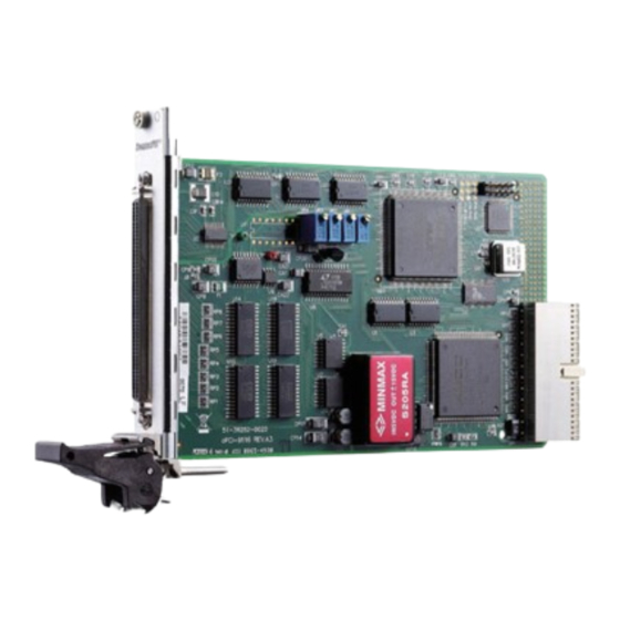
Page 19: Cpci-9116 And Cpci-9116R Layout
Layout Figure 1: PCB Layout of the cPCI-9116 Installation • 9... -
Page 20: Figure 2: Pcb Layout Of Cpci-9116R And Rear I/O Adaptor
Figure 2: PCB Layout of cPCI-9116R and Rear I/O adaptor 10 • Installation... -
Page 21: Pci Configuration
PCI Configuration 1. Plug and Play: As a plug and play component, the board requests an interrupt number via a system call. The system BIOS responds with an interrupt assignment based on the board information and on known system parameters. These system parameters are determined by the installed drivers and the hardware load seen by the system. -
Page 22: Chapter 3 Signal Connections
Figure 3.1. With the REAR I/O adaptor specifically designed for the cPCI-9116R, the cPCI-9116R connector pin assignments are identical to that of the cPCI-9116. The red LED positioned on the front panel is used as a power indicator. -
Page 23: Figure 3: J1 Pin Assignments
J1 100-pin SCSI-type connector U_CMMD AGND AIH0 AI32 AIL0 AIH1 AI33 AIL1 AIH2 AI34 AIL2 AIH3 AI35 AIL3 AIH4 AI36 AIL4 AIH5 AI37 AIL5 AIH6 AI38 AIL6 AIH7 AI39 AIL7 AIH8 AI40 AIL8 AIH9 AI41 AIL9 AIH10 AI10 AI42 AIL10 AIH11 AI11 AI43... -
Page 24: Table 1. Legend Of J1 Connector
Legend of J1: Signal Name Definition U_CMMD User Common Mode Analog Input Channel n (single-ended) AIHn Analog High Input Channel n (differential) AILn Analog Low Input Channel n (differential) Digital Input Signal Channel n Digital Output Signal Channel n ExtTimeBase External Timebase Clock Input ExtTrg External Digital Trigger Signal... -
Page 25: Analog Input Signal Connection
Analog Input Signal Connection The 9116 series provides up to 64 single-ended or 32 differential analog input channels. You can set and fill the Channel Gain Queue to get the desired combination of the input signal types. The analog signals can be converted to digital value by the A/D converter. -
Page 26: Figure 5: Ground-Referenced Source And Differential Input
Differential input mode The differential input mode provides two inputs that respond to signal voltage differences between them. If the signal source is ground- referenced, the differential mode can be used for common-mode noise rejection. Figure 5 shows the connection of ground-referenced signal sources under differential input mode. -
Page 27: Digital I/O Connection
User Common Mode (U_CMMD) To measure ground-referenced signal sources, which are connected to the same ground point, you can connect the signals in a User-Common-Mode (U_CMMD) configuration. Fig 7 illustrates the connections. The signal local ground reference is connected to the negative input of the instrumentation Amplifier, and the common-mode ground potential to signal ground. -
Page 28: Chapter 4 Registers
Registers The descriptions of the registers and structure of the PCI-9116 are outlined in this chapter. The information in this chapter will assist programmers, who wish to handle the card with low-level programs. In addition, the low level programming syntax is introduced. This information can help beginners to operate the PCI-9116 in the shortest possible time. -
Page 29: Table 2. I/O Port Address
I/O Address Read Write Base + 0x00 Scan Interval Counter Scan Interval Counter Base + 0x04 Sample Interval Counter Sample Interval Counter Base + 0x08 Scan Counter Scan Counter Base + 0x0C DIV Counter DIV Counter Base + 0x10 Delay1 Counter Delay1 Counter Base + 0x14 M Counter... -
Page 30: Internal Timer/Counter Register
Internal Timer/Counter Register The 9116 series card basically has 6 counters, which are responsible for the scan timing of the analog input data acquisition. The 6 counters occupy 6 I/O address locations in the 9116 card as shown below. Address: BASE + 0 ~ BASE + 14 Attribute: read / write Data Format: Base + 0x00... -
Page 31: General Purpose Timer/Counter Register
General Purpose Timer/Counter Register One 16-bit, general-purpose timer/counter exists in the 9116 series card. Writing to this register loads the initial count value into the general-purpose timer/counter. Reading from this register feedbacks the current count value of the general-purpose timer/counter Address: BASE + 0x18 Attribute: write / read Data Format:... -
Page 32: General Purpose Timer/Counter Control Register
General Purpose Timer/Counter Control Register Address: BASE + 0x20 Attribute: write only Data Format: Counter Clk_sr MODE Gate_src MODE1 Down Down Table 5. General Purpose Timer/Counter Control Register Counter en (bit7): GPTC0 count enable 1: enable GPTC0 0: disable GPTC0 UpDown (bit6): GPTC0’s up/down pin software control 1: Up counter... -
Page 33: A/D Data Registers
Clk_src (bit3): GPTC0’s clock source 1: External Input (Pin 96) 0: Internal Timebase MODE1~MODE0 (bit1 ~ bit0): GPTC0’s Mode selection MODE1 MODE0 Description General Counter Pulse Generation Table 6. GPTC0’s Mode selection A/D Data Registers The digital converted data is 16-bits and is stored into 32-bit registers. Address: BASE +24 Attribute: read Data Format:... -
Page 34: Channel Gain Queue Register
Channel Gain Queue Register This register is used to fill the Channel Gain Queue. We recommend users use our call function to avoid any possible errors from these settings. Address: BASE + 0x24 Attribute: write Data Format: EN0 HL_sel UNIP DIFF U_CMMD Gain1 Gain0... -
Page 35: A/D & Fifo Control Register
HL_sel(bit3): >31 channel selection (single ended) 1: when channel number is larger than 31 0: when channel number is smaller than or equal to 31 DIFF(bit1): Analog Input Signals Type 1: Differential 0: Single ended UNIP(bit2): Analog Input Signals Polarity 1: Unipolar 0: Bipolar U_CMMD (bit0): User Defined Common Mode Selection... - Page 36 DMA (Bit8): Write Only, set for DMA transfer SC_dis (Bit7): Write Only, set to disable the SC counter Clear Channel Gain Queue (Bit6): Write Only Clear the Channel Gain Queue 0: no effect on the Channel Gain Queue 1: clear the Channel Gain Queue Set done (Bit5): Write Only 0: indicate the Channel Gain Queue is not ready 1: indicate the Channel Gain Queue is OK...
-
Page 37: A/D & Fifo Status Register
A/D & FIFO Status Register Address: BASE + 28 Attribute: read Data Format: Full HFull Empty Trg_det SC_TC ADOR ADOS Table 11. A/D & FIFO Status Register ACQ (Bit7): Read Only, set when acquisition is in progress. Full (Bit6): Read Only A/D FIFO Full status (Fatal Error!) 0: FIFO Full 1: FIFO not Full HFull(Bit5): Read only A/D FIFO Half Full status... -
Page 38: Digital I/O Register
SC_TC(Bit2) : Read/ Write 1 to clear Scan Counter Terminal Count Status 1: Scan Counter counts to 0 0: Scan Counter not completed ADOR(Bit1) : Read/ Write 1 to clear A/D Overrun Status (Fatal Error !) 1: A/D Overrun 0: A/D not Overrun ADOS(Bit0) : Read/ Write 1 to clear A/D Over Speed Status (Warning !) 1: A/D Over Speed 0: A/D not Over Speed... -
Page 39: A/D Trigger Mode Register
Address: BASE + 30 Attribute: write Data Format: Table 13. Digital I/O register (Write) 4.10 A/D Trigger Mode Register Address: BASE + 0x34 Attribute: write only Data Format: Time Retrig DLYSRC TrgP MODE2 MODE1 MODE0 Base softconv ACQ_EN M_enable Table 14. A/D Trigger Mode Register Registers •... -
Page 40: Table 15. Trigger Mode Selection Bits
softconv (bit10): ADC direct conversion control 1: generate 1 convert pulse 0: no effect ACQ_EN (bit9): Acquisition enable bit 1: enable the acquisition timing 0: disable the acquisition timing M_enable (bit8): M counter enable bit 1: ignore trigger signals before M counter reaches 0 0: accept the trigger signal anytime Retrig (bit7): Re-triggerability in an acquisition 1: Re-triggerable... -
Page 41: Interrupt Control Register
4.11 Interrupt Control Register Address: BASE + 0x38 Attribute: write Data Format: Clr_Timer Clr_STTC Clr_Hfull Clr_DTrg Clr_EOC Timer_en STTC_en Hfull_en DTrg_en EOC_en Table 16. Interrupt Control Register Timer_en (bit12): General Purpose Timer Interrupt Enable Control 1: Enable 0: Disable SCTC_en (bit11): Trigger Complete Interrupt Enable Control 1: Enable 0: Disable Hfull_en (bit10): A/D FIFO Half Full Interrupt Enable Control... - Page 42 EOC_en (bit8): End of conversion Interrupt Enable Control 1: Enable 0: Disable Clr_Timer (bit4): write 1 to clear the GPTC Interrupt status 1: clear interrupt from the GPTC 0: no effect Clr_SCTC (bit3): write 1 to clear the SCTC Interrupt 1: clear the interrupt on terminal count of the Scan counter 0: no effect...
-
Page 43: Interrupt Status Register
4.12 Interrupt Status Register Address: BASE + 0x38 Attribute: read Data Format: Timer STTC Hfull DTrg Table 17. Interrupt Status Register Timer (bit4): GPTC generated Interrupt status 1: Interrupt Occurs 0: Interrupt not Occur SCTC(bit3): Scan Counter reach Terminal Count Interrupt status 1: Interrupt Occurs 0: Interrupt not Occur HFull (bit2): data FIFO Half Full Interrupt... -
Page 44: Chapter 5 Operation Theory
Operation Theory The operation theory of the functions on the 9116 series is described in this chapter. The functions include the A/D conversion, Digital I/O and General Purpose Counter / Timer. The operation theory can help you better understand how to configure and program the 9116 series card. A/D Conversion 5.1.1 A/D Conversion Procedure... -
Page 45: Software Conversion With Polling Data Transfer Acquisition Mode (Software Polling)
5.1.2 Software conversion with polling data transfer acquisition mode (Software Polling) This is the easiest way to acquire a single A/D data. The A/D converter starts a conversion when the user writes 1 into bit10 of the A/D trigger mode register (BASE+34). -
Page 46: Specifying Channels, Gains, And Input Configurations In The Channel Gain Queue
5.1.2.1 Specifying Channels, Gains, and input configurations in the Channel Gain Queue In both Software Polling and programmable scan acquisition mode, the channel, gain, and input configuration (single-end, differential, and U_CMMD), where you want to acquire samples from, can be specified in the Channel Gain Queue. -
Page 47: Figure 9: Scan Timing
Timebase clock source In scan acquisition mode, all the A/D conversions start on the output of counters, which use Timebase as the clock source. With the software you can specify the Timebase to be either an internal clock source (on board 24MHz) or an external clock input on pin 45 of J1. -
Page 48: Specifying Channels, Gains, And Input Configurations In The Channel Gain Queue
Note: 1.The maximum A/D sampling rate is 250kHz. Therefore, SI2_counter can’t be smaller than 96 while using the internal Timebase. 2.The SI_counter is a 24-bit counter and the SI2_counter is a 16-bit counter. Therefore, the maximum scan interval while using the internal Timebase = /24M s = 0.699s, and the maximum sampling interval between 2 channels while using the internal Timebase = 2 /24M s = 2.73ms. -
Page 49: 5.1.3.3 Trigger Modes
Then Acquisition sequence of channels: 1, 2, 0, 2, 1, 2, 0, 2, 1, 2, 0, 2. Sampling Interval = 240/24M s = 10 us Scan Interval = 960/24M s = 40 us Equivalent sampling rate of ch0, ch1: 25kHz Equivalent sampling rate of ch2: 50kHz 5.1.3.3 Trigger Modes There are 5 trigger modes (software-trigger, pre-trigger, post-trigger,... -
Page 50: Figure 10: Pre-Trigger (Trigger Occurs After M Scans)
(M_counter = M = 3, DIV_counter=4, SC_counter=0) ExtTrg(pin46) Scan_start AD_conversion Scan_in_progress (SSH_OUT)(pin47) Acquisition_in_progress Aquired data Acquired & stored data (M scans) Operation start Figure 10: Pre-trigger (trigger occurs after M scans) Note: If an external trigger event occurs when a scan is in progress, the data acquisition won’t stop until this scan completes, and the stored M scans of data include the last scan. -
Page 51: Figure 12: Pre-Trigger With M_Enable = 0
When an external trigger signal occurs before the first M scans of data are converted, the amount of stored data could be fewer than the originally specified amount of DIV_counter * M_counter, as illustrated in fig 12. This situation can be avoided by setting M_enable. If M_enable is set to 1, the trigger signal will be ignored until the first M scans of data are converted, and it assures user of obtaining M scans of data under pre-trigger mode, as illustrated in fig 13. -
Page 52: Figure 13: Pre-Trigger With M_Enable = 1
(M_counter = M = 3, DIV_counter=4, SC_counter=0) The first M scans Trigger signals which occur in the shadow region(the first M scans) will be ignored ExtTrg(pin46) Scan_start AD_conversion Scan_in_progress (SSH_OUT )(pin47) Acquisition_in_progress Aquired data Acquired & stored data (M scans) Operation start Figure 13: Pre-trigger with M_enable = 1 Note: The SC_counter must be set to 0 in pre-trigger acquisition mode. -
Page 53: Figure 14: Middle Trigger With M_Enable = 1
(M_Counter=M=3, DIV_Counter=4, SC_Counter=N=1) The first M scans Trigger signals which occur in the shadow region(the first M scans) will be ignored ExtTrg(pin46) Scan_start AD_conversion Scan_in_progress ( SSH_OUT )(pin47) Acquisition_in_progress Aquired data M scans before N scans trigger after trigger Operation start Acquired &... -
Page 54: Figure 15: Middle Trigger (Trigger With Scan Is In Progress)
(M_Counter=M=2, DIV_Counter=4, SC_Counter=N=2) Trigger occurs when a scan is in progress ExtTrg(pin46) Scan_start AD_conversion Scan_in_progress (SSH_OUT)(pin47) Acquisition_in_progress Acquired data M scans before N scans trigger after trigger Operation start Acquired & stored data (M+N scans) Figure 15: Middle trigger (trigger with scan is in progress) Post-Trigger Acquisition Use post-trigger acquisition in applications where you want to collect data after an external trigger event. -
Page 55: Figure 17: Delay Trigger
Delay Trigger Acquisition Use delay trigger acquisition in applications where you want to delay the data collection after the occurrence of a specified trigger event. The delay time is controlled by the value, which is pre-loaded in the Delay_counter (16bit). The counter counts down on the rising edge of Delay_counter clock source after the trigger condition is met. -
Page 56: Figure 18: Post Trigger With Re-Trigger
Post-Trigger or Delay-trigger Acquisition with re-trigger Use post-trigger or delay-trigger acquisition with re-trigger function in applications where you want to collect data after several external trigger events. The number of scans after each trigger is specified in SC_counter, and users could program Retrig_no to specify the number of re-triggers. -
Page 57: A/D Data Transfer Modes
5.1.4 A/D Data Transfer Modes After the end of the A/D conversion, A/D data are buffered into the Data FIFO memory. The FIFO size on the 9116 series card is 1024 (1K) words. If the sampling rate is 10 KHz, the FIFO can buffer 102.4 ms of analog signal. After the FIFO is full, any data after this time will be lost. -
Page 58: Digital Input And Output
DMA Transfer PCI bus-mastering DMA is necessary for high speed DAQ in order to utilize the maximum PCI bandwidth. The bus -mastering controller, which is built-in into the AMCC-5933 PCI controller, controls the PCI bus when it becomes the master on the bus. Bus mastering reduces the size of the on-board memory and reduces the CPU loading because data is directly transferred to the computer’s memory without host CPU intervention. -
Page 59: General Purpose Timer/Counter Operation
General Purpose Timer/Counter Operation An independent 16-bit up/down timer/counter is designed in the FPGA for user applications. Fig 19 shows a simplified model of the timer/counter on the 9116 series card. It has the following features: CPCI-9116 Controller Initial Mode... -
Page 60: Figure 20: Mode 0 Operation
• Two programmable timer modes are provided: Mode 0: Interrupt on Terminal Count Mode 0 is typically used for event counting, as illustrated in fig 20. After the initial count is written, OUT is initially low, and will remain low until the Counter counts to zero. -
Page 61: Chapter 6 Software Utility & Calibration
The utility is described in the following sections. Note that the software driver for the cPCI-9116 and cPCI-9116R are the same. Running 9116util.exe program After finishing the DOS installation, you can execute the utility by typing the following command. -
Page 62: Calibration
****** cPCI-9116 Utility Rev. 1.0 ****** Copyright © 2001-2002, ADLINK Technology Inc. All rights reserved. <F1> : Calibration. <F2> : Function testing. <Esc>: Quit. >>> Select function key F1 ~ F2, or press <Esc> to quit. <<< Figure 22: CPCI-9116 Utility Main Screen... -
Page 63: Vr Assignment
9116 series card and the Variable Resister (VR) that needs to be adjusted will blink. ****** cPCI-9116 Calibration ****** <1> A/D PGA offset adjusting <2> A/D (Bipolar Gain = 1, -5V ~ 5V) adjusting <3>... -
Page 64: 6.2.3.1 Pga Offset Calibration
6.2.3.1 PGA offset Calibration 1. Short the A/D channel 0 (pin 2 of J1) to ground (pin51 of J1). 2. Use multi -meter to measure the voltage between TP1 and TP2 on board. 3. Adjust VR4 to obtain the multi-meter value as close as possible to 0V. 6.2.3.2 Bipolar input Calibration 1. -
Page 65: Figure 24: Cpci-9116 Function Testing Screen
<Esc>: Quit. Select 0 to 9 or <Esc> to quit function testing Figure 24: cPCI-9116 Function Testing Screen A calibration utility is supported in the software CD that is included in the product package. The calibration procedures and descriptions can be found in the utility. -
Page 66: Warranty Policy
Warranty Policy Thank you for choosing ADLINK. To understand your rights and enjoy all the after-sales services we offer, please read the following carefully. 1. Before using ADLINK’s products, please read the user manual and follow the instructions exactly. When sending in damaged products for repair, please attach an RMA application form. - Page 67 4. Customers are responsible for the fees regarding transportation of damaged products to our company or to the sales office. 5. To ensure the speed and quality of product repair, please download an RMA application form from our company website www.adlinktech.com Damaged products with RMA forms a ttached receive priority.
Need help?
Do you have a question about the cPCI-9116 and is the answer not in the manual?
Questions and answers