Sign In
Upload
Manuals
Brands
ADLINK Technology Manuals
Computer Hardware
cPCI-9116
ADLINK Technology cPCI-9116 Manuals
Manuals and User Guides for ADLINK Technology cPCI-9116. We have
2
ADLINK Technology cPCI-9116 manuals available for free PDF download: User Manual
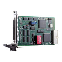
ADLINK Technology cPCI-9116 User Manual (67 pages)
64 Ch, 16 bit, 250KS/s Analog input Card For 3U Compact PC
Brand:
ADLINK Technology
| Category:
Computer Hardware
| Size: 0 MB
Table of Contents
Table of Contents
5
Tables
7
How to Use this Guide
9
Chapter 1 Introduction
11
Features
11
Applications
12
Specifications
13
Software Support
15
Programming Library
15
PCIS-LVIEW: Labview ® Driver
16
Daqbench TM : Activex Controls
16
Chapter 2 Installation
17
What You Have
17
Unpacking
18
Cpci-9116 and Cpci-9116R Layout
19
Figure 1: PCB Layout of the Cpci-9116
19
Figure 2: PCB Layout of Cpci-9116R and Rear I/O Adaptor
20
PCI Configuration
21
Chapter 3 Signal Connections
22
Connectors and Pin Assignment
22
Figure 3: J1 Pin Assignments
23
Table 1. Legend of J1 Connector
24
Analog Input Signal Connection
25
Types of Signal Sources
25
Input Configurations
25
Figure 4: Single-Ended Mode and Floating Sources
25
Figure 5: Ground-Referenced Source and Differential Input
26
Figure 6: Floating Source and Differential Input
26
Digital I/O Connection
27
Figure 7: Ground-Referenced Source and User Common Mode Connections
27
Figure 8: Digital I/O Connection
27
Chapter 4 Registers
28
I/O Port Address
28
Table 2. I/O Port Address
29
Internal Timer/Counter Register
30
Table 3. Timer/Counter Register Address
30
General Purpose Timer/Counter Register
31
Table 4. General Purpose Timer/Counter Register
31
General Purpose Timer/Counter Control Register
32
Table 5. General Purpose Timer/Counter Control Register
32
A/D Data Registers
33
Table 6. Gptc0'S Mode Selection
33
Table 7. A/D Data Registers
33
Channel Gain Queue Register
34
Table 8. Channel Gain Queue Register
34
Table 9. Gain Selection Bits
34
A/D & FIFO Control Register
35
Table 10. A/D & FIFO Control Register
35
A/D & FIFO Status Register
37
Table 11. A/D & FIFO Status Register
37
Digital I/O Register
38
Table 12. Digital I/O Register (Read)
38
A/D Trigger Mode Register
39
Table 13. Digital I/O Register (Write)
39
Table 14. A/D Trigger Mode Register
39
Table 15. Trigger Mode Selection Bits
40
Interrupt Control Register
41
Table 16. Interrupt Control Register
41
Interrupt Status Register
43
Table 17. Interrupt Status Register
43
Chapter 5 Operation Theory
44
A/D Conversion
44
A/D Conversion Procedure
44
Software Conversion with Polling Data Transfer Acquisition Mode (Software Polling)
45
Specifying Channels, Gains, and Input Configurations in the Channel Gain Queue
46
Programmable Scan Acquisition Mode
46
5.1.3.1 Scan Timing and Procedure
46
Figure 9: Scan Timing
47
Specifying Channels, Gains, and Input Configurations in the Channel Gain Queue
48
5.1.3.3 Trigger Modes
49
Figure 10: Pre-Trigger (Trigger Occurs after M Scans)
50
Figure 11: Pre-Trigger (Trigger with Scan Is in Progress)
50
Figure 12: Pre-Trigger with M_Enable = 0
51
Figure 13: Pre-Trigger with M_Enable = 1
52
Figure 14: Middle Trigger with M_Enable = 1
53
Figure 15: Middle Trigger (Trigger with Scan Is in Progress)
54
Figure 16: Post Trigger
54
Figure 17: Delay Trigger
55
Figure 18: Post Trigger with Re-Trigger
56
A/D Data Transfer Modes
57
Digital Input and Output
58
General Purpose Timer/Counter Operation
59
Figure 19: General-Purpose Timer/Counter Model
59
Figure 20: Mode 0 Operation
60
Figure 21: Mode 1 Operation
60
Chapter 6 Software Utility & Calibration
61
Running 9116Util.exe Program
61
Calibration
62
What Do You Need
62
Figure 22: CPCI-9116 Utility Main Screen
62
VR Assignment
63
6.2.3 A/D Adjustment
63
Figure 23: A/D Adjustment Menu Screen
63
Table 18. Functions of Vrs
63
6.2.3.1 PGA Offset Calibration
64
6.2.3.2 Bipolar Input Calibration
64
6.2.3.3 Unipolar Input Calibration
64
Functional Testing
64
Figure 24: Cpci-9116 Function Testing Screen
65
Warranty Policy
66
Advertisement
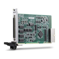
ADLINK Technology cPCI-9116 User Manual (50 pages)
64-ch, 16-bit, 250KS/s Analog Input Card for 3U CompactPCI
Brand:
ADLINK Technology
| Category:
Computer Hardware
| Size: 1 MB
Table of Contents
Table of Contents
5
List of Figures
7
List of Tables
9
1 Introduction
11
Features
11
Applications
12
Specifications
12
Analog Input
12
Digital I/O (DIO)
14
General Purpose Timer/Counter
14
General Specifications
14
Software Support
15
Figure 1-1: ADLINK MAPS Architecture
15
Figure 1-2: ADLINK Connection Explorer (ACE)
16
MAPS Core
16
Figure 1-3: ACE Soft Front Panel
17
MAPS/LV, Labview Support
17
MAPS/C, C & C++ Support
18
2 Installation
19
What You Have
19
Unpacking
20
Cpci-9116 Layout
21
Figure 2-1: PCB Layout of the Cpci-9116
21
PCI Configuration
22
Plug and Play
22
Configuration
22
Troubleshooting
22
3 Signal Connections
23
Connectors and Pin Assignment
23
100-Pin SCSI-Type Connector (J1)
24
Figure 3-1: J1 Pin Assignments
24
J1 Connector Legend
25
Analog Input Signal Connection
25
Types of Signal Sources
26
Input Configurations
26
Figure 3-2: Single-Ended Mode and Floating Sources
26
Figure 3-3: Ground-Referenced Source and Differential Input
27
Figure 3-4: Floating Source and Differential Input
27
Digital I/O Connection
28
Figure 3-6: Digital I/O Connection
28
4 Operation Theory
29
A/D Conversion Procedure
29
Conversion in Software Polling Mode
29
Channel Gain Queue Configuration
30
Programmable Scan Acquisition Mode
31
Scan Timing and Procedure
31
Figure 4-1: Scan Timing
32
Channel Gain Queue Configuration
33
Trigger Modes
34
Figure 4-2: Pre-Trigger (Trigger Occurs after M Scans)
35
Figure 4-3: Pre-Trigger (Trigger with Scan Is in Progress)
35
Figure 4-4: Pre-Trigger with M_Enable = 0 (before M Scans)
36
Figure 4-5: Pre-Trigger with M_Enable = 1
37
Figure 4-6: Middle Trigger with M_Enable = 1
38
Figure 4-7: Middle Trigger (Trigger with Scan Is in Progress)
39
Figure 4-8: Post Trigger
40
Figure 4-9: Delay Trigger
41
Figure 4-10: Post Trigger with Re-Trigger
42
A/D Data Transfer Modes
43
Digital Input and Output
44
General Purpose Timer/Counter Operation
45
Figure 4-11: General-Purpose Timer/Counter Model
45
Figure 4-12: Mode 0 Operation
46
Figure 4-13: Mode 1 Operation
46
Important Safety Instructions
47
Getting Service
50
Advertisement
Related Products
ADLINK Technology cPCI-9116R
ADLINK Technology NuDAQ cPCI-9112
ADLINK Technology NuDAQ cPCI-9112R
ADLINK Technology cPCI-3970 series
ADLINK cPCI-3510D
ADLINK Technology cPCI-3510L
ADLINK Technology cPCI-3510M
ADLINK Technology cPCI-6530V
ADLINK Technology cPCIS-1100 Series
ADLINK Technology cPCIS-6400U Series
ADLINK Technology Categories
Computer Hardware
Motherboard
PCI Card
Control Unit
Desktop
More ADLINK Technology Manuals
Login
Sign In
OR
Sign in with Facebook
Sign in with Google
Upload manual
Upload from disk
Upload from URL