Table of Contents
Advertisement
Quick Links
Introduction
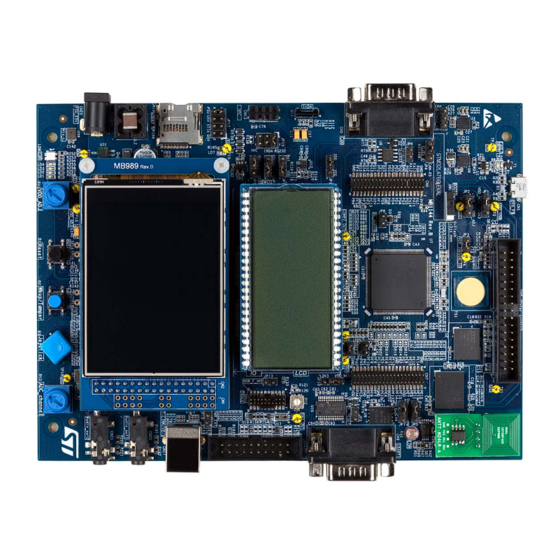
The STM32L476G-EVAL Evaluation board is designed as a complete demonstration and
development platform for the STMicroelectronics Arm
STM32L476ZG microcontroller with three I
port, SWPMI, two SAI ports, 12-bit ADC, 12-bit DAC, LCD driver, internal 128-Kbyte SRAM,
1-Mbyte flash memory, Quad-SPI port, touch sensing capability, USB OTG FS port, LCD
controller, flexible memory controller (FMC), JTAG debug port.
STM32L476G-EVAL, shown in
development, although it is not considered the final application.
A full range of hardware features on the board helps users to evaluate all on-board
peripherals such as USB, USART, digital microphones, ADC and DAC, dot-matrix TFT LCD,
LCD glass module, IrDA (supported up to version MB1144 C-01 of the board), LDR, SRAM,
NOR flash memory device, Quad-SPI flash memory device, microSD™ card, sigma-delta
modulators, smartcard with SWP, CAN transceiver, EEPROM, RF-EEPROM. Extension
headers allow connecting daughterboards or wrapping boards.
ST-LINK/V2-1 in-circuit debugger and flashing facility are integrated on the main board.
1. Picture not contractual.
June 2023
Evaluation board with STM32L476ZG MCU
Figure
1, is used as a reference design for user application
Figure 1. STM32L476G-EVAL Evaluation board
UM1855 Rev 6
®
Cortex
®
-M4 core-based
²
C buses, three SPI and six USART ports, CAN
UM1855
User manual
www.st.com
1/80
1
Advertisement
Table of Contents

Related Manuals for ST STM32L476ZG


Summary of Contents for ST STM32L476ZG
-
Page 1: Figure 1. Stm32L476G-Eval Evaluation Board
NOR flash memory device, Quad-SPI flash memory device, microSD™ card, sigma-delta modulators, smartcard with SWP, CAN transceiver, EEPROM, RF-EEPROM. Extension headers allow connecting daughterboards or wrapping boards. ST-LINK/V2-1 in-circuit debugger and flashing facility are integrated on the main board. Figure 1. STM32L476G-EVAL Evaluation board 1. Picture not contractual. -
Page 2: Table Of Contents
6.1.2 ST-LINK/V2-1 firmware upgrade ......16 ETM trace ..........16 Power supply . - Page 3 UM1855 Contents 6.8.2 STM32L476G-EVAL used as a USB Host ..... . . 25 6.8.3 Configuration elements related to the USB OTG FS port ... 26 6.8.4 Limitations in using the USB OTG FS port .
- Page 4 ST-LINK/V2-1 programming connector (CN16) ....67 ST-LINK/V2-1 Type-B USB connector (CN17) ..... 67 JTAG connector (CN15) .
- Page 5 UM1855 Contents 7.10 ADC/DAC connector (CN8) ........70 7.11 RF-EEPROM daughterboard connector (CN3) .
- Page 6 List of tables UM1855 List of tables Table 1. Ordering information ............10 Table 2.
- Page 7 UM1855 List of tables Table 49. Product history ............76 Table 50.
- Page 8 List of figures UM1855 List of figures Figure 1. STM32L476G-EVAL Evaluation board ......... 1 Figure 2.
-
Page 9: Features
Features • STM32L476ZG microcontroller with 1-Mbyte flash memory and 128-Kbyte RAM • Four power supply options: power jack, ST-LINK/V2-1 USB connector, USB OTG FS connector, daughterboard • Microcontroller supply voltage: 3.3 V or range of 1.71 to 3.6 V •... -
Page 10: Ordering Information
Ordering information UM1855 Ordering information To order the STM32L476G-EVAL Evaluation board, refer to Table 1. Additional information is available from the datasheet and reference manual of the target microcontroller. Table 1. Ordering information Order code Board references Target STM32 – MB1144 –... -
Page 11: Development Environment
• STMicroelectronics - STM32CubeIDE Demonstration software Demonstration software is preloaded in the STM32L476ZG flash memory, for easy demonstration of the device peripherals in Standalone mode. For more information and to download the latest available version, refer to the STM32L476G-EVAL demonstration software available on the www.st.com... -
Page 12: Unpacking Recommendations
In particular, pay attention to the following components: Quartz crystal (X2 position) microSD™ card in its receptacle (CN18) RF-EEPROM board (ANT7-M24LR-A) in its connector (CN3) For product information related to the STM32L476ZG microcontroller, visit the www.st.com website. 12/80 UM1855 Rev 6... -
Page 13: Hardware Layout And Configuration
UM1855 Hardware layout and configuration Hardware layout and configuration The STM32L476G-EVAL Evaluation board is designed around the STM32L476ZG target microcontroller in an LQFP 144-pin package. Figure 2 illustrates STM32L476ZG connections with peripheral components. Figure 3 shows the location of the main components on the Evaluation board. -
Page 14: Figure 3. Stm32L476G-Eval Main Component Layout
LCD glass module daughterboard DB979 IrDA CN12 Trace CN13 CN15 JTAG CN19 TFT LCD CN18 Standard-B microSD card USB port of ST-LINK/V2-1 CN20 Headphones 1 CN22 jack Power jack CN21 Headphones 2 U36 left jack microphone U35 right Four LEDs microphone... -
Page 15: St-Link/V2-1
STM32L476ZG. Section 6.3 provides more detail on powering STM32L476G-EVAL. For full detail on both versions of the debug and flashing tool, the standalone ST-LINK/V2 and the embedded ST-LINK/V2-1, refer to www.st.com. 6.1.1 Drivers Before connecting STM32L476G-EVAL to a Windows ®... -
Page 16: St-Link/V2-1 Firmware Upgrade
ETM trace The connector CN12 can output trace signals used for debugging. By default, the Evaluation board is configured such that STM32L476ZG PE2 to PE5 signals are not connected to trace outputs Trace_D0, Trace_D1, Trace_D2, Trace_D3, and Trace_CK of CN12. They are used for other functions. -
Page 17: Power Supply
PC informs the ST-LINK/V2-1 facility of its capability to supply up to 300 mA of current. If the answer is positive, the ST-LINK/V2-1 sets the ST890 switch (U37) to the ON position to supply power to the remainder of the STM32L476G-EVAL board. If the PC USB port cannot supply up to 300 mA of current, the power jack (CN22) can be used to supply the board. -
Page 18: Using St-Link/2-1 Along With Powering Via The Power Jack (Cn22)
The board might require more than 300 mA of supply current. It cannot be supplied from the host PC connected to the ST-LINK/2-1 USB port for debugging or flashing STM32L476ZG. In such a case, the board can be supplied through CN22 (marked PSU _E5V on the board). -
Page 19: Table 5. Power-Supply-Related Jumper Settings
UM1855 Hardware layout and configuration Table 5. Power-supply-related jumper settings Jumper array Jumper setting Configuration JP17 STM32L476G-EVAL is supplied via the power jack marked PSU_E5V (CN22). The extension connector (CN6) does not pass the 5 V of STM32L476G-EVAL to the daughterboard. JP17 STM32L476G-EVAL is supplied through the Micro-AB USB connector (CN1). - Page 20 VDD_MCU connection VDD_MCU is connected to voltage in the range of +1.71 to +3.6 V, adjustable with potentiometer RV1. JP10 Default setting. VDDA terminal of STM32L476ZG is connected to JP10 VDD_MCU. VDDA JP10 connection VDDA terminal of STM32L476ZG is connected to +3.3 V.
-
Page 21: Clock References
UM1855 Hardware layout and configuration Clock references Two clock references are available on STM32L476G-EVAL for the STM32L476ZG target microcontroller: • 32.768 kHz crystal X1, for embedded RTC • 8 MHz crystal X2, for main clock generator The main clock can also be generated using an internal RC oscillator. The X2 crystal is in a socket. -
Page 22: Boot
RAM, for debugging The microcontroller is configured to one of the listed boot options by setting the STM32L476ZG port BOOT0 level by the switch SW1 and by setting the nBOOT1 bit of FLASH_OPTR option bytes register, as shown in Table 8. -
Page 23: Bootloader Limitations
Refer to this document and follow the description of the bootloader versions and limitations. Audio A codec connected to the SAI interface of STM32L476ZG supports the TDM feature of the SAI port. TDM feature offers STM32L476ZG the capability to stream two independent stereo audio channels to two separate stereo analog audio outputs, simultaneously. -
Page 24: Headphones Outputs
Identical or different stereo audio content can be played back in each set of headphones. The STM32L476ZG sends up to two independent stereo audio channels, via its SAI1 TDM port, to the audio codec device. The codec device converts the digital audio stream to stereo analog signals. -
Page 25: Limitations In Using Audio Features
Section 6.22: NOR flash memory device. • If the SAI1 port of STM32L476ZG is used for streaming audio to the WM8994 codec IC, STM32L476ZG cannot control the motor. • If the digital microphones are attached to STM32L476ZG, the LCD glass module cannot be driven. -
Page 26: Configuration Elements Related To The Usb Otg Fs Port
PB12 and PB13 ports of STM32L476ZG - NFC, touch sensing, motor control, SWP. The PB12 and PB13 ports of STM32L476ZG are not required for the USB OTG FS port to operate as a USB Device. Table 11. Configuration elements related to the USB OTG FS port... -
Page 27: Limitations In Using The Usb Otg Fs Port
6.8.5 Operating voltage The USB-related operating supply voltage of STM32L476ZG (VDD_USB line) must be within the range of 3.0 to 3.6 V. RS-232 and IrDA ports The STM32L476G-EVAL board offers one RS-232 communication port and one IrDA port. -
Page 28: Rs-232 Port
RS-232 port The RS-232 communication port uses the DE-9M 9-pole connector (CN9). RX, TX, RTS, and CTS signals of the USART1 port of STM32L476ZG are routed to CN9. bootloader_RESET_3V3 and Bootloader_BOOT0_3V3 signals can also be routed to CN9, for ISP (in-system programming) support. To route Bootloader_RESET_3V3 to CN9, the R93 resistor must be removed and the JP9 jumper closed (open by default). -
Page 29: Lpuart Port
In the default configuration of STM32L476G-EVAL, the RX and TX terminals of the LPUART port are routed to the USB Virtual COM port of ST-LINK/V2-1, and the RX and TX terminals of the USART1 port to the RS-232 connector (CN9). -
Page 30: Operating Voltage
Motor control The CN2 connector is designed to receive a motor-control (MC) module. Table 15 shows the assignment of CN2 and STM32L476ZG terminals. Table 15 also lists the modifications to be made on the board versus its by-default configuration. See Section 6.12.1... - Page 31 UM1855 Hardware layout and configuration Table 15. Motor control terminal and function assignment (continued) Motor control STM32L476ZG microcontroller connector (CN2) Terminal Alternate Board modifications for Terminal Port name Function name function enabling motor control PhaseA Close SB34 ADC123_IN current+ Remove MB979 daughterboard...
-
Page 32: Board Modifications To Enable Motor Control
Hardware layout and configuration UM1855 6.12.1 Board modifications to enable motor control Figure 7 (top side) and Figure 8 (bottom side) illustrate the board modifications listed in Table 15, required for the operation of motor control. The red color denotes a component to be removed. -
Page 33: Limitations
The 9-pole male connector (CN5) of the DE-9M type is available as a CAN interface. A 3.3 V CAN transceiver is fitted between the CN5 connector and the CAN controller port of STM32L476ZG. The JP4 jumper allows selecting one of the High-speed, Standby, and Slope-control modes of the CAN transceiver. -
Page 34: Limitations
The CN6 and CN7 headers complement the LCD glass module daughterboard connector, to give access to all GPIOs of the STM32L476ZG microcontroller. In addition to GPIOs, the following signals and power supply lines are also routed on CN6 or CN7: •... -
Page 35: Figure 9. Lcd Glass Module Daughterboard In Display Position
LCD glass module daughterboard. In its display function, STM32L476ZG terminals are routed to LCD segments. In its I/O-bridge function, they are not. Instead, they transit from one row of CN11 pins to the other and from one row of CN14 pins to the other, thanks to interconnections fitted by the LCD glass module daughterboard. -
Page 36: Table 17. Lcd-Daughterboard-Related Configuration Elements
Hardware layout and configuration UM1855 Figure 10. LCD glass module daughterboard in I/O-bridge position Table 17. LCD-daughterboard-related configuration elements Setting to enable Element LCD glass Description segment module PA1 routed to LCDSEG0 SEG0 SB32 Open PA1 not routed to motor control PA2 routed to LCDSEG1 SEG1 SB31... - Page 37 UM1855 Hardware layout and configuration Table 17. LCD-daughterboard-related configuration elements (continued) Setting to enable Element LCD glass Description segment module PB11 routed to LCDSEG11 SEG11 Open PB11 not routed to Quad-SPI flash memory device PB12 routed to LCDSEG12 SEG12 Open PB12 not routed to Quad-SPI flash memory device PB13 routed to LCDSEG13 SEG13...
-
Page 38: Table 18. Lcd Glass Element Mapping - Segments 0 To 9
Hardware layout and configuration UM1855 corresponding to each COMx and SEGy combination. Names in quoting marks denote elements forming textual symbols, for example, “µA” or “+”. Figure 11 shows the physical location and shape of each segment on the LCD glass module. Table 18. -
Page 39: Limitations
UM1855 Hardware layout and configuration Table 21. LCD glass element mapping - segments 30 to 39 SEG30 SEG31 SEG32 SEG33 SEG34 SEG35 SEG36 SEG37 SEG38 SEG39 COM0 COM1 COM2 COM3 COM4 COM5 COM6 COM7 6.15.1 Limitations LCD glass module operation is exclusive to all other features of the board. UM1855 Rev 6 39/80... -
Page 40: Figure 11. Lcd Glass Display Element Mapping
Figure 11. LCD glass display element mapping 3a 4a 5a 6a 7a 8a 9a 10a 11a 12a 13a 14a 15a 16a 17a 18a 10j 11j 12j 13j 14j 15j 16j 17j 18j MSv36961V1... -
Page 41: Tft Lcd Panel
The TFT LCD panel is attached to the 16-bit data bus and accessed with FMC. The base address is 0x6800 0000, corresponding to NOR/SRAM3 bank1. The panel is selected with the LCD_NE3 chip select signal generated by the PG10 port of the STM32L476ZG. Address lines A0 and A1 determine the panel resources addressed, as depicted in... -
Page 42: User Leds
Table 25 shows the assignment of ports routed to the physical input devices. They are either ports of the STM32L476ZG or of one of the two I/O expander ICs on the board, named, in the schematic diagrams, IOExpander1 and IOExpander2. -
Page 43: Limitations
As illustrated in the schematic diagram, the PB4 port is routed, in the STM32L476ZG, to the noninverting input of comparator Comp2. The PA0 is routed to the noninverting input of the operational amplifier OpAmp1. However, depending on register settings, it can also be routed to ADC1 or ADC2. -
Page 44: Comparator
DAC output low-pass filter formed with R73 and C47 can be modified by replacing these components according to application requirements. The VREF+ terminal of STM32L476ZG is used as a reference voltage for both ADC and DAC. By default, it is routed to VDDA through a jumper fitted into the two-way header (CN10). -
Page 45: Limitations
UM1855 Hardware layout and configuration By removal of R18, a zero-ohm resistor, the SRAM is deselected and the STM32L476ZG ports PD7, PE0, and PE1 corresponding to FMC_NE1, FMC_NBL0 and FMC_NBL1 signals, respectively, can be used for other application purposes. Table 27. SRAM chip select configuration... -
Page 46: Limitations
Element Setting Configuration Default setting. R53 In PD6 port of STM32L476ZG is used for SAI1_SDA signal and routed to SB10 open audio codec. NOR flash memory device’s status register can be accessed. SB10 PD6 port of STM32L476ZG is used for the FMC_NWAIT signal and R53 Out routed to NOR flash memory device’s RB port. -
Page 47: Quad-Spi Flash Memory Device
SB13 MB979 SB12 closed QSPI_D0 data line is available at Quad-SPI flash memory device: SB13 open PB1 port of STM32L476ZG is routed to the DQ0 port of the Quad-SPI MB979 out flash memory device. Default setting. SB14 open QSPI_D1 data line is not available at Quad-SPI flash memory device:... -
Page 48: Limitations
An active shield is designed in layer two of the main PCB, under the button footprint. It allows the reduction of disturbances from other circuits to prevent false touch detections. The active shield is connected to the PC6 port of STM32L476ZG through the resistor R37. The related charge capacitor is connected to PC7. -
Page 49: Table 30. Touch-Sensing-Related Configuration Elements
PC6 is routed to the active shield under the touch-sensing button. Closed This setting is good for the robustness of touch sensing. Default setting. PC6 port of STM32L476ZG is not routed to motor Open control. This setting is good for the robustness of touch sensing. -
Page 50: Limitations
EVAL main board, in the U30 position. This interface performs all supply protection and control functions of the smartcard. This interface device is controlled, in its turn, by STM32L476ZG, directly through its ports or indirectly through the ports of the U33 I/O expander device (IOExpander2), as shown in... -
Page 51: Table 32. Configuration Elements Related To Smartcard And Swp
UM1855 Hardware layout and configuration Table 32. Configuration elements related to smartcard and SWP Element Setting Configuration Default setting. R109 in Smartcard SWP cannot be handled: R39 in PB12 is routed to the USB OTG FS port as the USBOTG_OVRCR SB3 open line, on top of being routed to the SWIO port of the smartcard CN11 I/O-bridged... -
Page 52: Limitations
Hardware layout and configuration UM1855 6.27.1 Limitations The following limitations apply to the smartcard operation: • Smartcard operation is mutually exclusive to the LCD glass module, the Quad-SPI flash memory device, and the motor control operation. • SWP operation is mutually exclusive to the LCD glass module, touch-sensing button, motor control, and USB OTG FS port operation if the last operates as a USB Host. -
Page 53: Dual-Channel Sigma-Delta Modulators Stpms2L
DAT port outputs converted measurement data on the DFSDM_DATIN1 line, received by the STM32L476ZG DFSDM controller. The data from STPMS2L are synchronized with the DFSDM_CKOUT clock generated by the STM32L476ZG DFSDM controller and received on the CLK terminal of STPMS2L. -
Page 54: Stpms2L Settings
Hardware layout and configuration UM1855 Figure 13. Routing of STPMS2L dual-channel sigma-delta modulators STM32L476ZGT6 STPMS2L Power metering DFSDM_DATIN1 STPMS2L PT100_DATIN Temperature metering PT100 DFSDM_CKOUT CLKOUT to MEMS microphones MSv36962V2 6.29.2 STPMS2L settings STPMS2L operating parameters are set through its configuration terminals MS0, MS1, MS2, and MS3. -
Page 55: Figure 14. Power Measurement Principle Schematic Diagram
UM1855 Hardware layout and configuration Figure 14. Power measurement principle schematic diagram to STPMS2L Shunt resistor "Current" AC source differential input 1 for current measurement Complex impedance to STPMS2L "Voltage" differential input 2 MSv38950V2 A low-voltage AC generator is to be applied by the user as shown in Figure 14. -
Page 56: Stpms2L For Pt100 Measurement
Hardware layout and configuration UM1855 Figure 15. STPMS2L power metering schematic diagram STPMS2 power metering 6.29.4 STPMS2L for PT100 measurement PT100 is a resistor with temperature-dependent resistance. Usually, one of two methods is used for measuring temperature with a temperature- dependent resistor. -
Page 57: Limitations
6.30 STM32L476ZG current consumption measurement STM32L476ZG has a built-in circuit allowing it to measure its current consumption (IDD) in Run and Low-power modes, except for Shutdown mode. It is strongly recommended that the MCU supply voltage (VDD_MCU line) does not exceed 3.3 V. -
Page 58: Figure 17. Schematic Diagram Of The Analog Part Of Idd Measurement
Hardware layout and configuration UM1855 R135 and R123. The former state is used for measuring the current consumption in Dynamic-Run mode, the latter in Low-power mode. The differential amplifier uses three stages U15B, U15C, and U15D of the quadruple operational amplifier device U15, TSZ124. The gain is set to 50, so an additional 50 mV at the U15C output, terminal 8 of U15 represents every 1 mA of supply current. -
Page 59: Low-Power Mode Idd Measurement Principle - Logic Part
UM1855 Hardware layout and configuration 6.30.2 Low-power mode IDD measurement principle - logic part The target microcontroller can only carry out actions for measuring a voltage when in Dynamic-Run mode. This is the reason why, a voltage representing the current consumed by the microcontroller when in Low-power mode needs to be held by a sample-and-hold circuit, which the microcontroller exploits later, when back in Dynamic-Run mode. -
Page 60: Idd Measurement In Dynamic-Run Mode
Hardware layout and configuration UM1855 Phase 3 - exiting Low-power mode, measurement, and end The MCU is in Low-power mode. The voltage across the C73 capacitor is now stabilized so it represents the current consumed by the MCU in Low-power mode. Phase 3 starts by setting the U13 path between ports O/I and I/O to a nonconductive state, for the voltage across C73 to hold. -
Page 61: Table 34. Jp11 Jumper Settings During Idd Measurement With Calibration
JP11 Configuration used to measure V offset JP11 in VDD position 1 2 3 4 STM32L476ZG supply current does not flow through the shunt resistor. JP11 Configuration to transit from direct to shunted supply to 1 2 3 4 JP11 STM32L476ZG, without ever interrupting the MCU supply. -
Page 62: Connectors
Connectors UM1855 Connectors RS-232 D-sub male connector (CN9) Figure 20. RS-232 D-sub (DE-9M) 9-pole connector (front view) MS30720V1 Table 35. RS-232 D-sub (DE-9M) connector (CN9) with HW flow control and ISP support Terminal Terminal name Terminal Description Bootloader_BOOT0 RS232_RX (PB7) RS232_TX (PG12) Bootloader_RESET Power connector (CN22) -
Page 63: Lcd Daughterboard Connectors (Cn11 And Cn14)
Evaluation boards. The width between CN11 pin 1 and CN14 pin 1 is 700 mils (17.78 mm). STM32L476ZG ports routed to these two connectors can be accessed on odd CN11 and CN14 pins (the row of pin 1) when no daughterboard is plugged in. -
Page 64: Extension Connectors (Cn6 And Cn7)
Connectors UM1855 Table 36. LCD daughterboard connectors (CN11 and CN14) (continued) CN11 CN14 Odd pin MCU port Odd pin MCU port Extension connectors (CN6 and CN7) Table 37. Daughterboard extension connector (CN6) Alternative How to disconnect Alternative functions to Description Functions use on the extension connector CODEC_INT,... -
Page 65: Table 38. Daughterboard Extension Connector (Cn7)
UM1855 Connectors Table 37. Daughterboard extension connector (CN6) (continued) Alternative How to disconnect Alternative functions to Description Functions use on the extension connector +3V3 LPUART_TX Remove R119, R189 PA11 USBOTG_DM Remove R3 Do not use Trace connector (CN12) and JTAG PA14 TCK/SWCLK connector (CN15) - Page 66 Connectors UM1855 Table 38. Daughterboard extension connector (CN7) (continued) Alternative How to disconnect Alternative functions to Description Functions use on the extension connector PE12 PE10 LED1, Remove R54, SB11 MC_DissipativeBrake PF12 Do not connect the NFC daughterboard to PF11 NFC_NSS connector (CN13).
-
Page 67: St-Link/V2-1 Programming Connector (Cn16)
It is not populated by default and is not for use by the end user. ST-LINK/V2-1 Type-B USB connector (CN17) The USB connector (CN17) is used to connect the onboard ST-LINK/V2-1 facility to the PC for flashing and debugging software. -
Page 68: Jtag Connector (Cn15)
Connectors UM1855 Table 39. USB Type-B connector (CN17) Terminal Description Terminal Description VBUS(power) Shield JTAG connector (CN15) Figure 23. JTAG debugging connector (CN15) top view MS30722V2 Table 40. JATG debugging connector (CN15) Terminal Function / MCU port Terminal Function / MCU port VDD power VDD power PA15... -
Page 69: Etm Trace Debugging Connector (Cn12)
UM1855 Connectors ETM trace debugging connector (CN12) Figure 24. Trace debugging connector (CN12) top view MS30722V2 Table 41. Trace debugging connector (CN12) Terminal Function / MCU port Terminal Function / MCU port VDD power TMS/PA13 TCK/PA14 TDO/PB3 TDI/PA15 RESET# TraceCLK/PE2 TraceD0/PE3 or SWO/PB3 TraceD1/PE4 or nTRST/PB4 TraceD2/PE5... -
Page 70: Microsd™ Card Connector (Cn18)
Connectors UM1855 microSD™ card connector (CN18) Figure 25. microSD™ card connector (CN18) Evaluation board microSD CN18 card MSv38995V1 Table 42. microSD™ card connector (CN18) Terminal Terminal name (MCU port) Terminal Terminal name (MCU port) SDIO_D2 (PC10) Vss/GND SDIO_D3 (PC11) SDIO_D0 (PC8) SDIO_CMD (PD2) SDIO_D1 (PC9) SDIO_CLK (PC12) -
Page 71: Rf-Eeprom Daughterboard Connector (Cn3)
UM1855 Connectors Table 43. Analog input-output connector (CN8) Terminal Function / MCU port Terminal Function / MCU port analog input-output PA4 7.11 RF-EEPROM daughterboard connector (CN3) Figure 27. RF-EEPROM daughterboard connector (CN3) front view MS30715V2 Table 44. RF-EEPROM daughterboard connector (CN3) Terminal Terminal name (MCU port) Terminal... -
Page 72: Usb Otg Fs Micro-Ab Connector (Cn1)
Connectors UM1855 Table 45. Motor control connector (CN2) Description MCU port MCU port Description terminal terminal Emergency STOP PWM_1H PWM_1L PWM_2H PWM_2L PWM_3H PWM_3L BUS VOLTAGE CURRENT A CURRENT B CURRENT C ICL Shutout DISSIPATIVE PCD Ind Current BRAKE Heat sink +5V power temperature PFC SYNC... -
Page 73: Can D-Sub Male Connector (Cn5)
Table 48. NFC terminal (CN13) assignment CN13 NFC signal MCU port Description terminal NFC_IRQOUTN or Interrupt output for NFC UART_TX Connected to STM32L476ZG UART RX NFC_IRQINN or Interrupt input for CR95HF UART_RX Connected to STM32L476ZG UART TX UM1855 Rev 6 73/80... - Page 74 Connectors UM1855 Table 48. NFC terminal (CN13) assignment (continued) CN13 NFC signal MCU port Description terminal NFC_NSS PF11 SPI slave select NFC_MISO PB14 SPI data, slave output NFC_MOSI PB15 SPI data, slave input NFC_SCK PB13 SPI serial clock +3V3 Main power supply/power supply for RF drivers Ground 74/80 UM1855 Rev 6...
-
Page 75: Stm32L476G-Eval Board Information
Parts marked as "ES" or "E" are not yet qualified and therefore not approved for use in production. ST is not responsible for any consequences resulting from such use. In no event will ST be liable for the customer using any of these engineering samples in production. -
Page 76: Stm32L476G-Eval Product History
STM32L476G-EVAL board information UM1855 STM32L476G-EVAL product history Table 49. Product history Order Product Product change Product details Product limitations code identification description MCU: – STM32L476ZGT6U revision “3, 4” MCU errata sheet: – STM32L476xx/STM32L4 86xx device limitations (ES0250) Boards: The product is delivered –... -
Page 77: Board Revision History
UM1855 STM32L476G-EVAL board information Board revision history Table 50. Board revision history Board variant and Board change Board reference Board limitations revision description DEFAULT-B02 Initial revision No limitation PCB change to avoid issues with BGA and silkscreen correction DEFAULT-C02 IrDA not supported LD5/LD6 and removed IrDA feature (U11 obsolete) -
Page 78: Federal Communications Commission (Fcc) And Ised Canada Compliance Statements
Federal Communications Commission (FCC) and ISED Canada Compliance Statements UM1855 Federal Communications Commission (FCC) and ISED Canada Compliance Statements FCC Compliance Statement 9.1.1 Part 15.19 This device complies with Part 15 of the FCC Rules. Operation is subject to the following two conditions: (1) this device may not cause harmful interference, and (2) this device must accept any interference received, including interference that may cause undesired operation. -
Page 79: Revision History
22-Jul-2015 Initial Version Added Section 6.6.2: Bootloader limitations. 29-Jul-2015 Classification change from ST Restricted to Public. Figure 3: swap of FAULT and VBUS prints in the upper-left corner of the board. Section 6.8.3: swap of LD5 and LD6. 9: modified Section 9.1.3... - Page 80 ST products and/or to this document at any time without notice. Purchasers should obtain the latest relevant information on ST products before placing orders. ST products are sold pursuant to ST’s terms and conditions of sale in place at the time of order acknowledgment.
Need help?
Do you have a question about the STM32L476ZG and is the answer not in the manual?
Questions and answers