Table of Contents
Advertisement
Quick Links
Evaluation board for STGAP4S advanced galvanically isolated gate driver
Introduction
The
STGAP4S
is a galvanically isolated single gate driver for IGBTs and SiC MOSFETs with advanced protection, configuration,
and diagnostic features. The architecture of the STGAP4S isolates the channel gate driving from the control and from the low
voltage interface circuitry through true galvanic isolation. The unique output architecture is designed to allow the use of an
external MOSFET push-pull stage giving flexibility in terms of current capability dimensioning and easing the use of several
power switches in parallel. The 2 pre-driver outputs are characterized by current capability and output voltage swing optimized
for that topology and allow the use of a negative gate driving supply.
The
EVALSTGAP4S
board allows to evaluate all the STGAP4S features. The board is equipped with two STGAP4S drivers
connected in an SPI daisy chain and with each high voltage side fed by its own flyback power supply, whose controller is
integrated in the driver itself. Each STGAP4S drives the gate of an SiC MOSFET in H2PAK-7 package having 650 V voltage
rating and connected in half-bridge.
Multiple EVALSTGAP4S boards can be connected together allowing the implementation of an SPI daisy chain with more than
two devices and also the evaluation of more complex topologies, as a full bridge inverter.
The use in combination with the STEVAL-PCC009V2 communication board allows the easy configuration of all the driver's
protection and control features, through the SPI interface, as well as access to the driver's status registers, offering an
advanced diagnostic. The board can be used also in standalone mode without a communication board using the default device
configuration at power-on.
UM3153 - Rev 1 - May 2023
For further information contact your local STMicroelectronics sales office.
UM3153
User manual
www.st.com
Advertisement
Table of Contents

Related Manuals for STMicroelectronics EVALSTGAP4S


Summary of Contents for STMicroelectronics EVALSTGAP4S
- Page 1 Each STGAP4S drives the gate of an SiC MOSFET in H2PAK-7 package having 650 V voltage rating and connected in half-bridge. Multiple EVALSTGAP4S boards can be connected together allowing the implementation of an SPI daisy chain with more than two devices and also the evaluation of more complex topologies, as a full bridge inverter.
-
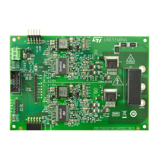
Page 2: Figure 1. Evalstgap4S Evaluation Board
UM3153 Figure 1. EVALSTGAP4S evaluation board UM3153 - Rev 1 page 2/28... -
Page 3: Safety And Operating Instructions
UM3153 Safety and operating instructions Safety and operating instructions General terms During assembly, testing, and operation, the evaluation board poses several inherent hazards, including bare wires, moving or rotating parts and hot surfaces. Danger: There is danger of serious personal injury, property damage or death due to electrical shock and burn hazards if the kit or components are improperly used or installed incorrectly. -
Page 4: Operating The Evaluation Board
UM3153 Operating the evaluation board Operating the evaluation board To properly operate the board, follow these safety rules. Work area safety: – The work area must be clean and tidy. – Do not work alone when boards are energized. – Protect against inadvertent access to the area where the board is energized using suitable barriers and signs. -
Page 5: Getting Started
Connect the STEVAL-PCC009V2 to the PC using the USB cable. • Turn on the VCC power supply (8 V<VCC<24 V) of the EVALSTGAP4S. The DIAG1 and DIAG2 LEDs turn • Connect the input signals IN+_H, IN+_L of EVALSTGAP4S J3 connector to the PWM function generator signals. -
Page 6: Evalstgap4S In Standalone Mode
2.2.2 Single board setup example • Connect the EVALSTGAP4S VCC power supply, present on J1 connector, to a power supply and turn it on (8 V<VCC<24 V). The DIAG1 and DIAG2 LEDs turn on. • Connect the input signals IN+_H, IN+_L of EVALSTGAP4S J3 connector to the PWM function generator signals. -
Page 7: Hardware Description And Configuration
Maximum working voltage across isolation: 1200 V The EVALSTGAP4S is provided with a linear regulator supplied by the VCC voltage that generates the 3.3 V supply for the low-voltage side of both the STGAP4S present on the board. The VCC voltage is also used to supply the two isolated flyback power supplies (one for each driver) that are driven by the controller integrated in each STGAP4S and generates the positive and negative voltages for the driving side. -
Page 8: Table 2. Jumper Resistor Description
UM3153 Hardware description and configuration Figure 2. Connectors location GNDPWR Table 2. Jumper resistor description Name Side Driver Function Both 3V3IN from on-board regulator JR3, JR5 Both Slave board power supply JR4, JR6 Both Master board power supply JR7, JR8, JR9, JR10 Both Cumulative diagnostic (DIAG1, DIAG2) JR11, JR12... -
Page 9: Figure 3. Jumper Location - Top Layer
UM3153 Hardware description and configuration Figure 3. Jumper location – TOP layer JR1 JR11 JR3 JR5 JR29 JR28 JR31 JR26 JR27 JR32 JR10 JR14 JR13 JR12 JR20 JR23 JR18 JR22 JR17 JR19 Figure 4. Jumper location – BOT layer JR30 JR21 UM3153 - Rev 1 page 9/28... -
Page 10: Table 3. Jumper Configuration Of 3V3In Power Supply Source
UM3153 Hardware description and configuration Table 3. Jumper configuration of 3V3IN power supply source Operating voltage Supply voltage source Jumper configurations Default configuration JR1 = CLOSE On-board regulator (from U3) JR3 = OPEN (VCC must be present, see Table JR4 = OPEN JR1 = OPEN External power supply (from J1) JR3 = OPEN... -
Page 11: Table 7. Jumper Configuration Of Pwm Input Signal (J3 Connector)
UM3153 Hardware description and configuration Default Operating voltage Supply voltage source Jumper configuration configuration JR27 = CLOSE VL_H = 0V (VCC must be present, see Table JR28 = CLOSE JR26 = DON’T CARE See STGAP4S Datasheet for External power supply (from J6) JR27 = CLOSE recommended values www.st.com... -
Page 12: Table 10. Jumper Configuration Of Spi Chain
UM3153 Hardware description and configuration Table 10. Jumper configuration of SPI chain Default Signal Function Jumper configuration configuration Configuration of SPI daisy chain loop with two devices (HS+LS) Suitable for: JR11 = CLOSE • single board configuration with two device daisy chain. SDO = SDO_H JR12 = OPEN Section 4... -
Page 13: Table 16. Jumper Configuration For High-Side Default Function
UM3153 Hardware description and configuration Name Function Jumper configuration Default configuration JR22 = OPEN DEFAULT_L DEFAULT PIN set HIGH JR23 = CLOSE Table 16. Jumper configuration for HIGH-side DEFAULT function Name Function Jumper configuration Default configuration JR31 = CLOSE DEFAULT PIN set LOW JR32 = OPEN DEFAULT_H JR31 = OPEN... - Page 14 UM3153 Hardware description and configuration Side Driver Connection TP29 Low-voltage High-side Flyback – MOSFET gate TP30 Low-voltage High-side Flyback – AUX T2 TP31 Low-voltage High-side Flyback – SNS_H TP32 Low-voltage High-side Flyback – COMP_H TP33 Low-voltage High-side TP34 Low-voltage High-side DIAG1_H TP35 Low-voltage...
-
Page 15: Single Board
Single board Single board The EVALSTGAP4S is provided with a ready-to-use SiC MOSFET half-bridge. The board must be supplied feeding the VCC voltage to the J1 connector. The VCC voltage is used to supply the flyback section of each driver and the on-board linear regulator that generates the 3V3IN for both the drivers. -
Page 16: Figure 6. Half-Bridge Configuration With Hardware Shoot-Through Protection
UM3153 Single board Figure 6. Half-bridge configuration with hardware shoot-through protection STGAP4S HS STGAP4S LS Figure 7. Single board configuration with independent inputs JR11=CLOSE Single board daisy chain with two devices JR1=CLOSE 3.3V from on-board linear regulator J1 - Power supply J9 - uC connection IN-_L IN-_H... -
Page 17: Multiple Boards Connection
Multiple boards connection Multiple boards connection To evaluate complex topologies, like a full inverter, it is possible to connect multiple EVALSTGAP4S boards through connectors J2 and J4. The drivers can be configured through the daisy chain connection of the SPI bus where the driver in the lowest board is the master and must be connected to the μC board using the J7 connector... -
Page 18: Power Supply Options
Power supply options Power supply options The EVALSTGAP4S board is provided with an on-board linear regulator to supply the 3V3IN of the LV side and a flyback circuit to supply the HV side. The linear regulator is fed by the VCC and generates a 3.3 V that is used to supply both the STGAP4S devices... -
Page 19: Figure 11. Flyback Power Supply (Default Setting)
UM3153 Power supply options As as shown in Figure 11, the VCC voltage feeds also the flyback converter that generates an isolated secondary voltage used to supply a post-regulator that stabilizes the HV side supply voltages to the following values: •... -
Page 20: Evalstgap4S Schematic Diagram
UM3153 EVALSTGAP4S schematic diagram EVALSTGAP4S schematic diagram Figure 13. EVALSTGAP4S schematic diagram - connectors UM3153 - Rev 1 page 20/28... -
Page 21: Figure 14. Evalstgap4S Schematic Diagram - Low-Side
UM3153 EVALSTGAP4S schematic diagram Figure 14. EVALSTGAP4S schematic diagram - low-side UM3153 - Rev 1 page 21/28... -
Page 22: Figure 15. Evalstgap4S Schematic Diagram - High-Side
UM3153 EVALSTGAP4S schematic diagram Figure 15. EVALSTGAP4S schematic diagram - high-side UM3153 - Rev 1 page 22/28... -
Page 23: Figure 16. Evalstgap4S Schematic Diagram - Power Stage
UM3153 EVALSTGAP4S schematic diagram Figure 16. EVALSTGAP4S schematic diagram - power stage UM3153 - Rev 1 page 23/28... -
Page 24: Revision History
UM3153 Revision history Table 18. Document revision history Date Version Changes 24-May-2023 Initial release. UM3153 - Rev 1 page 24/28... -
Page 25: Table Of Contents
EVALSTGAP4S schematic diagram ........ -
Page 26: List Of Tables
UM3153 List of tables List of tables Table 1. Connector description..............7 Table 2. -
Page 27: List Of Figures
EVALSTGAP4S schematic diagram - connectors ........ - Page 28 IMPORTANT NOTICE – READ CAREFULLY STMicroelectronics NV and its subsidiaries (“ST”) reserve the right to make changes, corrections, enhancements, modifications, and improvements to ST products and/or to this document at any time without notice. Purchasers should obtain the latest relevant information on ST products before placing orders. ST products are sold pursuant to ST’s terms and conditions of sale in place at the time of order acknowledgment.
Need help?
Do you have a question about the EVALSTGAP4S and is the answer not in the manual?
Questions and answers