Table of Contents
Advertisement
Quick Links
Chipsmall Limited consists of a professional team with an average of over 10 year of expertise in the distribution
of electronic components. Based in Hongkong, we have already established firm and mutual-benefit business
relationships with customers from,Europe,America and south Asia,supplying obsolete and hard-to-find components
to meet their specific needs.
With the principle of "Quality Parts,Customers Priority,Honest Operation,and Considerate Service",our business
mainly focus on the distribution of electronic components. Line cards we deal with include
Microchip,ALPS,ROHM,Xilinx,Pulse,ON,Everlight and Freescale. Main products comprise
IC,Modules,Potentiometer,IC Socket,Relay,Connector.Our parts cover such applications as commercial,industrial,
and automotives areas.
We are looking forward to setting up business relationship with you and hope to provide you with the best service
and solution. Let us make a better world for our industry!
Contact us
Tel: +86-755-8981 8866 Fax: +86-755-8427 6832
Email & Skype: info@chipsmall.com Web: www.chipsmall.com
Address: A1208, Overseas Decoration Building, #122 Zhenhua RD., Futian, Shenzhen, China
Advertisement
Table of Contents

Related Manuals for Altera DE2i-150


Summary of Contents for Altera DE2i-150
- Page 1 Chipsmall Limited consists of a professional team with an average of over 10 year of expertise in the distribution of electronic components. Based in Hongkong, we have already established firm and mutual-benefit business relationships with customers from,Europe,America and south Asia,supplying obsolete and hard-to-find components to meet their specific needs.
-
Page 3: Table Of Contents
CONTENTS Chapter 1 Introduction of the FPGA System of DE2i-150 Board......5 1-1 Layout and Components ..........................5 1-2 Block Diagram of the DE2i-150 Board...................... 7 Chapter 2 DE2i-150 Control Panel ................ 10 2-1 Control Panel Setup..........................10 2-2 Controlling the LEDs, 7-segment Displays and LCD Display .............. 12 2-3 Switches and Push-buttons ........................ - Page 4 3-14 Implementing a TV Encoder ........................50 3-15 Using IR ..............................50 3-16 Using SSRAM/SDRAM/FLASH/SD Card .................... 51 Chapter 4 DE2i-150 System Builder ..............58 4-1 Introduction .............................. 58 4-2 General Design Flow ..........................58 4-3 Using DE2i-150 System Builder ......................59 Chapter 5 Examples of Advanced Demonstrations ..........
- Page 5 7-2 Making HAL CFI Flash drivers to work with Spansion F-lash ............. 109 7-3 Revision History............................. 110 7-4 Copyright Statement ..........................110...
-
Page 6: Chapter 1 Introduction Of The Fpga System Of De2I-150 Board
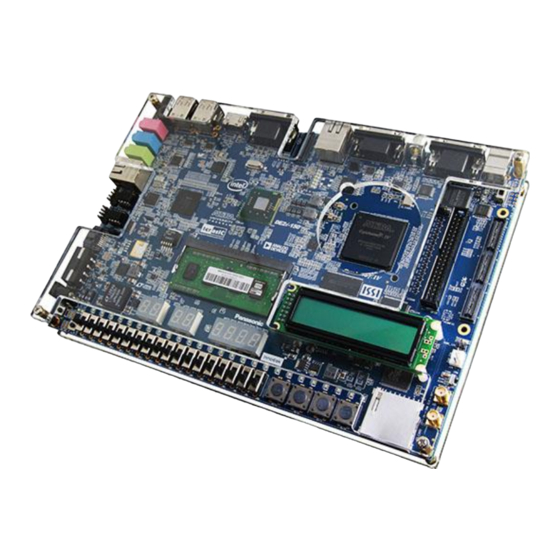
Chapter 1 Introduction of the FPGA System of DE2i-150 Board This chapter presents the features and design characteristics of the DE2i-150 board. A photograph of the DE2i-150 board is shown in Figure 1-1 Figure 1-2. It depicts the layout of the board and indicates the location of the connectors and key components. - Page 7 Figure 1-2 The DE2i-150 board (bottom view) The DE2i-150 board has many features that allow users to implement a wide range of designed circuits, from simple circuits to various multimedia projects. The following hardware (FPGA System) is provided on the DE2i-150 board: ...
-
Page 8: Block Diagram Of The De2I-150 Board
DE2i-150 board. In order to use the DE2i-150 board, the user has to be familiar with the Quartus II software. The necessary knowledge can be acquired by reading the tutorials “... - Page 9 Following is more detailed information about the blocks in Figure 1-3: o Cyclone IV EP4CGX150DF31 device o 149,760 LEs o 720 M9K memory blocks o 6,480 Kbits embedded memory o 8 PLLs o JTAG and AS mode configuration o EPCS64 serial configuration device o On-board USB Blaster circuitry o 128MB (32Mx32bit) SDRAM o 4MB (1Mx32) SSRAM...
- Page 10 o 18 slide switches and 4 push-buttons switches o 18 red and 9 green LEDs o 8 7-segment displays o Infrared remote-control receiver module o TV decoder (NTSC/PAL/SECAM) and TV-in connector...
-
Page 11: Chapter 2 De2I-150 Control Panel
Chapter 2 DE2i-150 Control Panel The DE2i-150 board comes with a Control Panel program that allows users to access various components on the board from a host computer. The host computer communicates with the board through a USB connection. The program can be used to verify the functionality of components on the board or be used as a debug tool while developing RTL code. - Page 12 2-2. The “Control Circuit” that Figure The concept of the DE2i-150 Control Panel is illustrated in performs the control functions is implemented in the FPGA board. It communicates with the Control Panel window, which is active on the host computer, via the USB Blaster link. The graphical interface is used to send commands to the control circuit.
-
Page 13: Controlling The Leds, 7-Segment Displays And Lcd Display
Figure 2-2 The DE2i-150 Control Panel concept The DE2i-150 Control Panel can be used to light up LEDs, change the values displayed on 7-segment and LCD displays, monitor buttons/switches status, read/write the SDRAM, SSRAM and Flash Memory, output VGA color pattern to VGA monitor, verify functionality of HSMC connector I/Os, communicate with PC via RS-232 interface, read SD Card specification information, and display the resolution measurement of 3-axis accelerometer on the G-Sensor. - Page 14 Figure 2-4. From the window, directly use the left-right arrows to control the 7-SEG patterns on the DE2i-150 board which are updated immediately. Note that the dots of the 7-SEGs are not enabled on DE2i-150 board. Figure 2-4 Controlling 7-SEG display...
-
Page 15: Switches And Push-Buttons
Figure 2-5 Controlling the LCD display The ability to set arbitrary values into simple display devices is not needed in typical design activities. However, it gives users a simple mechanism for verifying that these devices are functioning correctly in case a malfunction is suspected. Thus, it can be used for troubleshooting purposes. -
Page 16: Sdram/Ssram/Flash Controller And Programmer
The Control Panel can be used to write/read data to/from the SDRAM, SSRAM and Flash chips on the DE2i-150 board. As an example, we will describe how the SDRAM may be accessed; the same approach is used to access the SSRAM, and Flash. Click on the Memory tab and select “SDRAM”... - Page 17 Figure 2-7 Accessing the SDRAM A 16-bit word can be written into the SDRAM by entering the address of the desired location, specifying the data to be written, and pressing the Write button. Contents of the location can be read by pressing the Read button.
-
Page 18: Sd Card
Choosing the SD Card tab leads to the window in Figure 2-8. Insert an SD Card to the DE2i-150 board, and then press the Read button to read the SD Card. The SD Card‟s identification, specification, and file format information will be displayed in the... -
Page 19: Rs-232 Communication
The Control Panel allows users to verify the operation of the RS-232 serial communication interface on the DE2i-150. The setup is established by connecting a RS-232 9-pin male to female cable from the PC to the RS-232 port where the Control Panel communicates to the terminal emulator software on the PC, or vice versa. -
Page 20: Vga
Figure 2-9 RS-232 Serial Communication DE2i-150 Control Panel provides VGA pattern function that allows users to output color pattern to LCD/CRT monitor using the DE2i-150 board. Follow the steps below to generate the VGA pattern function: Choosing the Video tab leads to the window in Figure 2-10. -
Page 21: Hsmc
HSMC connector. Before running the HSMC loopback verification test, follow the instruction noted under the Loopback Installation section and click on Verify. Please note to turn off the DE2i-150 board before the HSMC loopback adapter is installed to prevent any damage to the board. -
Page 22: Ir Receiver
Figure 2-11 HSMC loopback verification test performed under Control Panel From the control panel, we can test the IR receiver on the DE2i-150 by sending scan code from a remote controller. Figure 2-12 depicts the IR receiver window when the IR tab is pressed. When the scan code is received, the information will be displayed on the IR Receiver window represented in hexadecimal. -
Page 23: G-Sensor
On the DE2i-150 board, the G-sensor function is being demonstrated by Spirit level .The user can rotate the DE2i-150 board to different directions, up or down, left or right. The bubble will travel quickly following your manners. Meanwhile, the control panel will show the accelerated data in... -
Page 24: Overall Structure Of The De2I-150 Control Panel
Figure 2-13 Testing the G-sensor The DE2i-150 Control Panel is based on a Nios II SOPC system instantiated in the Cyclone IV GX FPGA with software running on the on-chip memory. The software part is implemented in C code; the hardware part is implemented in Verilog HDL code with SOPC builder. The source code is not available on the DE2i_150 System CD. - Page 25 Figure 2-14 The block diagram of the DE2i-150 control panel...
-
Page 26: Chapter 3 Using The De2I-150 Board
This chapter gives instructions for using the DE2i-150 board and describes each of its peripherals. In the DE2i-150 power up sequence, there is a monitor circuit that monitors the status of the FPGA configuration. After it confirms the configuration is complete, the power up sequence will go to next state.
Need help?
Do you have a question about the DE2i-150 and is the answer not in the manual?
Questions and answers