
Related Manuals for Altera Arria V GX FPGA


Summary of Contents for Altera Arria V GX FPGA
- Page 1 Arria V GX FPGA Development Board Reference Manual Arria V GX FPGA Development Board Reference Manual 101 Innovation Drive San Jose, CA 95134 www.altera.com MNL-01067-1.1 Feedback Subscribe Arrow.com. Downloaded from...
- Page 2 © 2013 Altera Corporation. All rights reserved. ALTERA, ARRIA, CYCLONE, HARDCOPY, MAX, MEGACORE, NIOS, QUARTUS and STRATIX words and logos are trademarks of Altera Corporation and registered in the U.S. Patent and Trademark Office and in other countries. All other words and logos identified as trademarks or service marks are the property of their respective holders as described at www.altera.com/common/legal.html.
-
Page 3: Table Of Contents
Featured Device: Arria V GX FPGA ........ - Page 4 How to Contact Altera ........
-
Page 5: Chapter 1. Overview
The Arria V GX FPGA development board provides a hardware platform for developing and prototyping low-power, high-performance, and logic-intensive designs using Altera’s Arria V GX FPGA device. The board provides a wide range of peripherals and memory interfaces to facilitate the development of Arria V GX FPGA designs. -
Page 6: Board Component Blocks
1–2 Chapter 1: Overview Board Component Blocks Board Component Blocks The development board features the following major component blocks: Two Arria V GX FPGA 5AGXFB3HF40 in the 1517-pin FineLine BGA (FBGA) ■ package 362 LEs ■ 136,880 adaptive logic modules (ALMs) ■... -
Page 7: Dual Fpga
1152-Mbyte (MB) DDR3 SDRAM with a 72-bit data bus ■ 4.5-MB QDRII+ SRAM ■ 1-Gbit (Gb) synchronous flash with a 16-bit data bus ■ November 2013 Altera Corporation Arria V GX FPGA Development Board Reference Manual Arrow.com. Arrow.com. Arrow.com. Arrow.com. Arrow.com. -
Page 8: Fpga 2
Memory ■ 1024-MB DDR3 SDRAM with a 64-bit data bus (soft controller) ■ 512-MB DDR3 SDRAM with a 32-bit data bus (hard IP controller) ■ Arria V GX FPGA Development Board November 2013 Altera Corporation Reference Manual Arrow.com. Arrow.com. Arrow.com. -
Page 9: Development Board Block Diagram
Eight MAX II control DIP switches ■ Development Board Block Diagram Figure 1–1 shows a block diagram of the Arria V GX FPGA development board. Figure 1–1. Arria V GX FPGA Development Board Block Diagram Port B Port A 2x16 LCD... - Page 10 1–6 Chapter 1: Overview Handling the Board Arria V GX FPGA Development Board November 2013 Altera Corporation Reference Manual Arrow.com. Arrow.com. Arrow.com. Arrow.com. Arrow.com. Arrow.com. Arrow.com. Arrow.com. Arrow.com. Arrow.com. Downloaded from Downloaded from Downloaded from Downloaded from Downloaded from Downloaded from...
-
Page 11: Introduction
2. Board Components Introduction This chapter introduces the major components on the Arria V GX FPGA development board. Figure 2–1 illustrates the component locations and Table 2–1 provides a brief description of all component features of the board. A complete set of schematics, a physical layout database, and GERBER files for the development board reside in the Arria V GX FPGA development kit documents directory. -
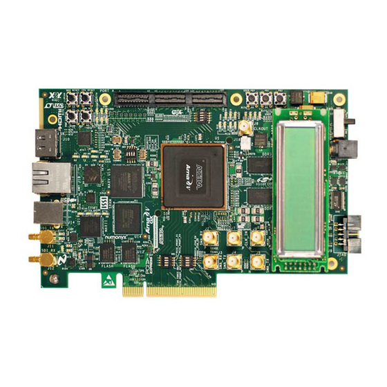
Page 12: Board Overview
2–2 Chapter 2: Board Components Board Overview Board Overview This section provides an overview of the Arria V GX FPGA development board, including an annotated board image and component descriptions. Figure 2–1 shows an overview of the available components. Figure 2–1. Overview of the Arria V GX FPGA Development Board Features... - Page 13 Chapter 2: Board Components 2–3 Board Overview Table 2–1. Arria V GX FPGA Development Board Components (Part 2 of 4) Board Reference Type Description FPGA 1 mode select DIP Sets the Arria V MSEL[4,2,1] pins. This switch is located on the switch bottom of the board.
- Page 14 2–4 Chapter 2: Board Components Board Overview Table 2–1. Arria V GX FPGA Development Board Components (Part 3 of 4) Board Reference Type Description Programmable oscillator with default frequencies of CLK0=625 MHz, CLK1=100 MHz, CLK2=625 MHz, CLK3=125 MHz at I...
- Page 15 Chapter 2: Board Components 2–5 Board Overview Table 2–1. Arria V GX FPGA Development Board Components (Part 4 of 4) Board Reference Type Description DDR3 SDRAM interface on FPGA 2. There are two interface options: Option 1: 512-MB interface with a 32-bit data bus. This DDR3 ■...
-
Page 16: Featured Device: Arria V Gx Fpga
Featured Device: Arria V GX FPGA Featured Device: Arria V GX FPGA The Arria V GX FPGA development board features two Arria V GX FPGA 5AGXFB3HF40 device (U13 and U16) in a 1517-pin FBGA package. For more information about Arria V device family, refer to the Arria V GX Device Handbook. -
Page 17: I/O Resources
Bank 4A Table 2–4 lists the Arria V GX FPGA 1 pin count and usage by function on the development board. Clocks are listed under special pins as it uses dedicated I/O pins. Table 2–4. Arria V GX FPGA 1 Pin Count and Usage (Part 1 of 2) - Page 18 2–8 Chapter 2: Board Components Featured Device: Arria V GX FPGA Table 2–4. Arria V GX FPGA 1 Pin Count and Usage (Part 2 of 2) Function I/O Standard I/O Count Special Pins Flash 1.8-V CMOS — PCI Express 2.5-V CMOS...
-
Page 19: Max Ii Cpld Epm2210 System Controller
Chapter 2: Board Components 2–9 MAX II CPLD EPM2210 System Controller Table 2–5. Arria V GX FPGA 2 Pin Count and Usage (Part 2 of 2) Function I/O Standard I/O Count Special Pins — — Chip-to-chip bridge — — Total Transceivers:... - Page 20 FM bus address FM_A4 1.8-V FM bus address FM_A5 1.8-V FM bus address FM_A6 1.8-V FM bus address FM_A7 Arria V GX FPGA Development Board November 2013 Altera Corporation Reference Manual Arrow.com. Arrow.com. Arrow.com. Arrow.com. Arrow.com. Arrow.com. Arrow.com. Arrow.com. Arrow.com.
- Page 21 FMC_C2M_PG 2.5-V FMC module to card power good FMC_M2C_PG 2.5-V FMC module present FMC_PRSNT 2.5-V FMC module clock FMC_SCL November 2013 Altera Corporation Arria V GX FPGA Development Board Reference Manual Arrow.com. Arrow.com. Arrow.com. Arrow.com. Arrow.com. Arrow.com. Arrow.com. Arrow.com. Arrow.com.
- Page 22 2.5-V FPGA 2 mode select 0 FPGA2_MSEL0 2.5-V FPGA 2 mode select 1 FPGA2_MSEL1 2.5-V FPGA 2 mode select 2 FPGA2_MSEL2 Arria V GX FPGA Development Board November 2013 Altera Corporation Reference Manual Arrow.com. Arrow.com. Arrow.com. Arrow.com. Arrow.com. Arrow.com. Arrow.com.
- Page 23 FPGA 1 fan RPM control OVERTEMP1 2.5-V FPGA 2 fan RPM control OVERTEMP2 2.5-V Load the flash memory image identified by the PGM LEDs PGM1_CONFIG November 2013 Altera Corporation Arria V GX FPGA Development Board Reference Manual Arrow.com. Arrow.com. Arrow.com. Arrow.com. Arrow.com. Arrow.com. Arrow.com.
- Page 24 Board Reference Description Manufacturer Part Number Website IC - MAX II CPLD EPM2210 Altera Corporation EPM2210F324 www.altera.com 324FBGA -3 LF 1.8V VCCINT Arria V GX FPGA Development Board November 2013 Altera Corporation Reference Manual Arrow.com. Arrow.com. Arrow.com. Arrow.com. Arrow.com. Arrow.com. Arrow.com.
-
Page 25: Configuration, Status, And Setup Elements
This configuration method implements a USB Type-AB connector (J7), a FTDI USB 2.0 PHY device (U5), and an Altera MAX II CPLD (U2) to allow the FPGA configuration using a USB cable that connects directly between the USB port on the board and a USB port of a PC running the Quartus II software. - Page 26 JTAG chain DIP switch (SW6). The interface in the JTAG chain depends on the switch settings but the FPGAs and MAX II devices are always in the JTAG chain. Arria V GX FPGA Development Board November 2013 Altera Corporation Reference Manual Arrow.com.
-
Page 27: Fpga Programming From Flash Memory
The PFL megafunction is a block of logic that is programmed into an Altera programmable logic device (FPGA or CPLD). The PFL functions as a utility for writing to a compatible flash memory device. This... - Page 28 '1'. Otherwise, the user hardware page 1 loads. Pressing the PGM1_CONFIG push button (S3) loads the FPGA with a hardware page based on which PGM1_LED[2:0] LED (D12, D13, D14) illuminates. Arria V GX FPGA Development Board November 2013 Altera Corporation Reference Manual Arrow.com.
-
Page 29: Fpga Programming Over External Usb-Blaster
D12, D13, page loads from flash memory when you press the PGM1_LED[2:0] — 2.5-V PGM1_SEL push button or when you power-on the board. November 2013 Altera Corporation Arria V GX FPGA Development Board Reference Manual Arrow.com. Arrow.com. Arrow.com. Arrow.com. Arrow.com. Arrow.com. - Page 30 AD17 2.5-V Express link width x4. Yellow LED. Configure this LED to display the PCI PCIE_LED_X8 AT16 2.5-V Express link width x8. Arria V GX FPGA Development Board November 2013 Altera Corporation Reference Manual Arrow.com. Arrow.com. Arrow.com. Arrow.com. Arrow.com. Arrow.com.
-
Page 31: Setup Elements
ON : Load the factory design from flash for Arria V FPGA 1 at power up. FACTORY_USER1 OFF : Load the user design from flash at power up. Unused FACTORY_USER2 November 2013 Altera Corporation Arria V GX FPGA Development Board Reference Manual Arrow.com. Arrow.com. Arrow.com. Arrow.com. -
Page 32: Jtag Settings Dip Switch
JTAG Settings DIP Switch The JTAG settings DIP switch (SW6) either remove or include devices in the active JTAG chain. However, the Arria V GX FPGA 1 is always in the JTAG chain. Table 2–13 lists the switch controls and its descriptions. -
Page 33: Cpu Reset Push Button
Industries CPU Reset Push Button Each Arria V GX FPGA has a CPU reset push button, CPU1_RESETn (S4) for FPGA 1 and (S8) for FPGA 2. Both these push button are inputs to the Arria V GX CPU2_RESETn FPGA DEV_CLRn pin and are open-drain I/Os from the MAX II CPLD System Controller. -
Page 34: Configuration Push Button
This section describes the board's clock inputs and outputs. On-Board Oscillators The development board includes fixed and programmable oscillators with a frequency of 50-MHz, 100-MHz, 125-MHz, 148.5-MHz, 156.25-MHz, and 625-MHz. Arria V GX FPGA Development Board November 2013 Altera Corporation Reference Manual Arrow.com. - Page 35 Figure 2–6 shows the default frequencies of all external clocks going to the Arria V GX FPGA development board. Figure 2–6. Arria V GX FPGA Development Board Clocks 50 MHz B u ffe r C L K IN _ M A X _ 5 0...
- Page 36 REFCLK2_A_QR1_N LVDS REFCLK0_A_QR0_P 625.000 MHz LVDS REFCLK0_A_QR0_N LVDS CLKINTOPA_P1 125.000 MHz Top edge FPGA 1 – memory LVDS CLKINTOPA_N1 Arria V GX FPGA Development Board November 2013 Altera Corporation Reference Manual Arrow.com. Arrow.com. Arrow.com. Arrow.com. Arrow.com. Arrow.com. Arrow.com. Arrow.com. Arrow.com.
-
Page 37: Off-Board Clock Input/Output
AM33 HSMB_CLK_IN_P1 LVDS input from the installed HSMC cable or HSMC board. Can also support 2x LVTTL inputs. LVDS/LVTTL AL33 HSMB_CLK_IN_N1 November 2013 Altera Corporation Arria V GX FPGA Development Board Reference Manual Arrow.com. Arrow.com. Arrow.com. Arrow.com. Arrow.com. Arrow.com. Arrow.com. - Page 38 SG-310SDF 25.0000M-B3 www.eea.epson.com 24-MHz crystal oscillator Epson FA-128 24.0000MB-W www.eea.epson.com Y1, Y2, Y4, Y5 25-MHz crystal oscillator Epson FA-128 25.0000MB-C www.eea.epson.com Arria V GX FPGA Development Board November 2013 Altera Corporation Reference Manual Arrow.com. Arrow.com. Arrow.com. Arrow.com. Arrow.com. Arrow.com. Arrow.com.
-
Page 39: General User Input/Output
Board references S5, S6, and S7 are push buttons that allow you to interact with the Arria V GX FPGA 1 while S9, S10, and S11 are for use with the Arria V GX FPGA 2. When you press and hold down the button, the device pin is set to logic 0; when you release the button, the device pin is set to logic 1. -
Page 40: User-Defined Dip Switches
Board references SW2 and SW3 are two sets of eight-pin DIP switches. There are no board-specific functions for these switches. Each of the Arria V GX FPGA have a set of user-defined DIP switch. When the switch is in the OFF position, a logic 1 is selected. -
Page 41: User-Defined Leds
Board references D18 through D25 and D26 through D33 are two sets of eight pairs user-defined LEDs. Each of the Arria V GX FPGA have a set of user-defined LEDs. The LEDs illuminate when a logic 0 is driven, and turns off when a logic 1 is driven. -
Page 42: Hsmc User-Defined Leds
HSMC daughtercards. The LEDs are driven by the Arria V GX FPGA. Table 2–31 lists the HSMC user-defined LED schematic signal names and their corresponding Arria V GX FPGA pin numbers. Table 2–31. HSMC User-Defined LED Schematic Signal Names and Functions Board Schematic... -
Page 43: Lcd
You can also use the header for debugging or other purposes. Table 2–33 summarizes the LCD pin assignments. The signal names and directions are relative to the Arria V GX FPGA. Table 2–33. LCD Pin Assignments, Schematic Signal Names, and Functions Board Arria V GX FPGA... -
Page 44: Sdi Video Output/Input
Table 2–36. Supported Output Standards for SD and HD Input SD_HD Input Supported Output Standards Rise TIme SMPTE 424M, SMPTE 292M Faster SMPTE 259M Slower Arria V GX FPGA Development Board November 2013 Altera Corporation Reference Manual Arrow.com. Arrow.com. Arrow.com. Arrow.com. Arrow.com. - Page 45 Table 2–38. SDI Cable Equalizer Lengths Data Rate (Mbps) Cable Type Maximum Cable Length (m) 1485 Belden 1694A 2970 November 2013 Altera Corporation Arria V GX FPGA Development Board Reference Manual Arrow.com. Arrow.com. Arrow.com. Arrow.com. Arrow.com. Arrow.com. Arrow.com.
- Page 46 3-Gbps HD/SD SDI cable driver with National Semiconductor LMH0303SQx www.national.com cable detect 3-Gbps HD/SD SDI adaptive cable National Semiconductor LMH0384SQ www.national.com equalizer Arria V GX FPGA Development Board November 2013 Altera Corporation Reference Manual Arrow.com. Arrow.com. Arrow.com. Arrow.com. Arrow.com. Arrow.com. Arrow.com.
-
Page 47: Components And Interfaces
This signal connects directly to a Arria V GX FPGA REFCLK input pin pair using DC coupling. This clock is terminated on the motherboard and therefore, no on-board termination is required. - Page 48 The JTAG and SMB are optional signals in the PCI Express specification. Therefore, the JTAG signal loopback from PCI Express TDI to PCI Express TDO and are not used on this board. The SMB signals are wired to the Arria V GX FPGA but are not required for normal operation.
- Page 49 Part Number Website 4.20-mm pitch header, 13 A per pin, dual row, Molex 50-34-8571 www.molex.com right angle, with PCB mounting flanges. November 2013 Altera Corporation Arria V GX FPGA Development Board Reference Manual Arrow.com. Arrow.com. Arrow.com. Arrow.com. Arrow.com. Arrow.com. Arrow.com.
-
Page 50: 10/100/1000 Ethernet
This development board supports 10/100/1000 base-T Ethernet using an external Marvell 88E1111 PHY and Altera Triple-Speed Ethernet MegaCore MAC function. The PHY-to-MAC interface employs RGMII using the Arria V GX FPGA LVDS pins in Soft-CDR mode at 1.25 Gbps transmit and receive. In 10-Mb or 100-Mb mode, the RGMII interface still runs at 1.25 GHz but the packet data is repeated 10 or 100 times. - Page 51 Manufacturing Manufacturer Board Reference Description Manufacturer Part Number Website Marvell Ethernet PHY BASE-T device 88E1111-B2-CAA1C000 www.marvell.com Semiconductor November 2013 Altera Corporation Arria V GX FPGA Development Board Reference Manual Arrow.com. Arrow.com. Arrow.com. Arrow.com. Arrow.com. Arrow.com. Arrow.com. Arrow.com. Arrow.com. Arrow.com. Arrow.com.
-
Page 52: Hsmc
HSMC cards. The LVDS channels can be used for CMOS signaling as well as LVDS. The HSMC is an Altera-developed open specification, which allows you to expand the functionality of the development board through the addition of daughtercards (HSMCs). - Page 53 1.5-V PCML Transceiver RX bit 0 HSMA_RX_P0 1.5-V PCML Transceiver TX bit 0n HSMA_TX_N0 1.5-V PCML Transceiver RX bit 0n HSMA_RX_N0 November 2013 Altera Corporation Arria V GX FPGA Development Board Reference Manual Arrow.com. Arrow.com. Arrow.com. Arrow.com. Arrow.com. Arrow.com. Arrow.com. Arrow.com.
- Page 54 AP12 LVDS or 2.5-V LVDS TX bit 6 or CMOS bit 28 HSMA_TX_D_P6 LVDS or 2.5-V LVDS RX bit 6 or CMOS bit 29 HSMA_RX_D_P6 Arria V GX FPGA Development Board November 2013 Altera Corporation Reference Manual Arrow.com. Arrow.com. Arrow.com.
- Page 55 LVDS or 2.5-V LVDS TX bit 14n or CMOS bit 66 HSMA_TX_D_N14 AC13 LVDS or 2.5-V LVDS RX bit 14n or CMOS bit 67 HSMA_RX_D_N14 November 2013 Altera Corporation Arria V GX FPGA Development Board Reference Manual Arrow.com. Arrow.com. Arrow.com. Arrow.com.
- Page 56 2.5-V CMOS Management serial data HSMB_SDA AH26 2.5-V CMOS Management serial clock HSMB_SCL AV34 2.5-V CMOS JTAG clock signal JTAG_TCK Arria V GX FPGA Development Board November 2013 Altera Corporation Reference Manual Arrow.com. Arrow.com. Arrow.com. Arrow.com. Arrow.com. Arrow.com. Arrow.com. Arrow.com.
- Page 57 LVDS or 2.5-V LVDS RX bit 6n or CMOS bit 31 HSMB_RX_D_N6 AM31 LVDS or 2.5-V LVDS TX bit 7 or CMOS bit 32 HSMB_TX_D_P7 November 2013 Altera Corporation Arria V GX FPGA Development Board Reference Manual Arrow.com. Arrow.com. Arrow.com. Arrow.com.
- Page 58 LVDS or 2.5-V LVDS RX bit 15 or CMOS bit 69 HSMB_RX_D_P15 AN32 LVDS or 2.5-V LVDS TX bit 15n or CMOS bit 70 HSMB_TX_D_N15 Arria V GX FPGA Development Board November 2013 Altera Corporation Reference Manual Arrow.com. Arrow.com. Arrow.com.
-
Page 59: Sfp+ Module
FPGA. These modules takes in serial data from the FPGA and transform them into optical signals. The Arria V GX FPGA development board includes one SFP+ cage assembly for the SFP+ port that is used by the device. -
Page 60: Fmc Connector
2.5-V CMOS Clock input or output 2 FMC_CLK_BIDIR_P2 AD22 2.5-V CMOS Clock input or output 2 FMC_CLK_BIDIR_N2 AU22 2.5-V CMOS Clock input or output 3 FMC_CLK_BIDIR_P3 Arria V GX FPGA Development Board November 2013 Altera Corporation Reference Manual Arrow.com. Arrow.com. Arrow.com. Arrow.com. Arrow.com. - Page 61 2.5-V CMOS Transmit channel (available in Arria V GT FPGA device) FMC_DP_M2C_N9 2.5-V CMOS Transmit channel FMC_DP_M2C_P0 2.5-V CMOS Transmit channel FMC_DP_M2C_P1 November 2013 Altera Corporation Arria V GX FPGA Development Board Reference Manual Arrow.com. Arrow.com. Arrow.com. Arrow.com. Arrow.com. Arrow.com.
- Page 62 2.5-V CMOS FMC data bus HPC bank A FMC_HA_N23 AH16 2.5-V CMOS FMC data bus HPC bank A FMC_HA_P0 AF16 2.5-V CMOS FMC data bus HPC bank A FMC_HA_P1 Arria V GX FPGA Development Board November 2013 Altera Corporation Reference Manual Arrow.com. Arrow.com. Arrow.com. Arrow.com. Arrow.com.
- Page 63 FMC_HB_N13 AP13 2.5-V CMOS FMC data bus HPC bank B FMC_HB_N14 AH12 2.5-V CMOS FMC data bus HPC bank B FMC_HB_N15 November 2013 Altera Corporation Arria V GX FPGA Development Board Reference Manual Arrow.com. Arrow.com. Arrow.com. Arrow.com. Arrow.com. Arrow.com. Arrow.com.
- Page 64 2.5-V CMOS FMC data bus LPC bank A FMC_LA_N4 2.5-V CMOS FMC data bus LPC bank A FMC_LA_N5 2.5-V CMOS FMC data bus LPC bank A FMC_LA_N6 Arria V GX FPGA Development Board November 2013 Altera Corporation Reference Manual Arrow.com. Arrow.com. Arrow.com.
- Page 65 2.5-V CMOS FMC data bus LPC bank A FMC_LA_P8 AH17 2.5-V CMOS FMC data bus LPC bank A FMC_LA_P9 2.5-V CMOS FMC data bus LPC bank A FMC_LA_P10 November 2013 Altera Corporation Arria V GX FPGA Development Board Reference Manual Arrow.com. Arrow.com. Arrow.com. Arrow.com. Arrow.com. Arrow.com.
- Page 66 Board Manufacturing Manufacturer Description Manufacturer Reference Part Number Website FMC pitch socket array assembly connector Samtec ASP-134486-01 www.samtec.com Arria V GX FPGA Development Board November 2013 Altera Corporation Reference Manual Arrow.com. Arrow.com. Arrow.com. Arrow.com. Arrow.com. Arrow.com. Arrow.com. Arrow.com. Arrow.com. Arrow.com.
-
Page 67: Bull's Eye Connector
LVDS or 2.5-V Transceiver channel SMA_B_TX_L15_N LVDS or 2.5-V Transceiver channel SMA_B_TX_L15_P LVDS or 2.5-V Transceiver channel SMA_B_TX_R6_N LVDS or 2.5-V Transceiver channel SMA_B_TX_R6_P November 2013 Altera Corporation Arria V GX FPGA Development Board Reference Manual Arrow.com. Arrow.com. Arrow.com. Arrow.com. Arrow.com. Arrow.com. Arrow.com. -
Page 68: Memory
Insertion/Extraction tool CAT-EX-SCC-01 Memory This section describes the development board’s memory interface support and also their signal names, types, and connectivity relative to the Arria V GX FPGA. The development board has the following memory interfaces: DDR3 ■ ■... - Page 69 Table 2–54 lists the DDR3A (x72 soft controller) pin assignments, signal names, and functions. The signal names and types are relative to the Arria V GX FPGA in terms of I/O setting and direction. Table 2–54. DDR3A Devices Pin Assignments, Schematic Signal Names, and Functions (Part 1 of 5)
- Page 70 1.5-V SSTL Class I Data bus byte lane DDR3A_DQ50 1.5-V SSTL Class I Data bus byte lane DDR3A_DQ51 1.5-V SSTL Class I Data bus byte lane DDR3A_DQ52 Arria V GX FPGA Development Board November 2013 Altera Corporation Reference Manual Arrow.com. Arrow.com. Arrow.com.
- Page 71 1.5-V SSTL Class I Data strobe N byte lane DDR3A_DQS_N5 1.5-V SSTL Class I Data strobe P byte lane DDR3A_DQS_P4 1.5-V SSTL Class I Data strobe P byte lane DDR3A_DQS_P5 November 2013 Altera Corporation Arria V GX FPGA Development Board Reference Manual Arrow.com. Arrow.com. Arrow.com. Arrow.com. Arrow.com.
- Page 72 1.5-V SSTL Class I Data bus byte lane DDR3A_DQ8 1.5-V SSTL Class I Data bus byte lane DDR3A_DQ9 1.5-V SSTL Class I Data bus byte lane DDR3A_DQ10 Arria V GX FPGA Development Board November 2013 Altera Corporation Reference Manual Arrow.com. Arrow.com. Arrow.com.
-
Page 73: Ddr3B/C For Fpga 2
Table 2–55 lists the DDR3B (x32 hard controller) pin assignments, signal names, and functions. The signal names and types are relative to the Arria V GX FPGA in terms of I/O setting and direction. Table 2–55. DDR3 x32 Devices Pin Assignments, Schematic Signal Names, and Functions (Part 1 of 3) - Page 74 1.5-V SSTL Class I Data strobe P byte lane DDR3B_DQS_P0 1.5-V SSTL Class I Data strobe P byte lane DDR3B_DQS_P1 DDR3B (U12) 1.5-V SSTL Class I Write mask byte lane DDR3B_DM2 Arria V GX FPGA Development Board November 2013 Altera Corporation Reference Manual Arrow.com. Arrow.com. Arrow.com. Arrow.com.
- Page 75 Table 2–56 lists the DDR3C (x64 soft controller) pin assignments, signal names, and functions. The signal names and types are relative to the Arria V GX FPGA in terms of I/O setting and direction. Table 2–56. DDR3 x64 Devices Pin Assignments, Schematic Signal Names, and Functions (Part 1 of 3)
- Page 76 Data strobe N byte lane DDR3C_DQS_N1 1.5-V SSTL Class I Data strobe P byte lane DDR3C_DQS_P0 1.5-V SSTL Class I Data strobe P byte lane DDR3C_DQS_P1 Arria V GX FPGA Development Board November 2013 Altera Corporation Reference Manual Arrow.com. Arrow.com. Arrow.com. Arrow.com. Arrow.com.
- Page 77 U18, U19, U21, 32M×16×8, 2 Gb, DDR3 memory Micron MT41J128M16HA-125:D www.micron.com U22, U28 16M×8×8, 1 Gb, DDR3 memory Micron MT41J128M8JP-125:G www.micron.com November 2013 Altera Corporation Arria V GX FPGA Development Board Reference Manual Arrow.com. Arrow.com. Arrow.com. Arrow.com. Arrow.com. Arrow.com. Arrow.com. Arrow.com. Arrow.com.
-
Page 78: Qdrii
1.8-V HSTL Echo clock N QDRII_CQ_N AT21 1.8-V HSTL Echo clock P QDRII_CQ_P AE28 1.8-V HSTL Write data bus QDRII_D0 Arria V GX FPGA Development Board November 2013 Altera Corporation Reference Manual Arrow.com. Arrow.com. Arrow.com. Arrow.com. Arrow.com. Arrow.com. Arrow.com. Arrow.com. - Page 79 Write clock N QDRII_K_N AF25 1.8-V HSTL Write clock P QDRII_K_P AD24 1.8-V HSTL Read data bus QDRII_Q0 November 2013 Altera Corporation Arria V GX FPGA Development Board Reference Manual Arrow.com. Arrow.com. Arrow.com. Arrow.com. Arrow.com. Arrow.com. Arrow.com. Arrow.com. Arrow.com. Arrow.com.
- Page 80 1.8-V HSTL Read data bus QDRII_Q35 AR25 1.8-V HSTL Read port select QDRII_RPSN AK24 1.8-V HSTL Write port select QDRII_WPSN Arria V GX FPGA Development Board November 2013 Altera Corporation Reference Manual Arrow.com. Arrow.com. Arrow.com. Arrow.com. Arrow.com. Arrow.com. Arrow.com. Arrow.com.
-
Page 81: Flash
Table 2–60 lists the flash pin assignments, signal names, and functions. The signal names and types are relative to the Arria V GX FPGA in terms of I/O setting and direction. Table 2–60. Flash Pin Assignments, Schematic Signal Names, and Functions (Part 1 of 2) - Page 82 Table 2–61. Flash Component Reference and Manufacturing Information Manufacturing Manufacturer Board Reference Description Manufacturer Part Number Website 512-Mbit synchronous flash Numonyx PC28F512P30BF www.numonyx.com Arria V GX FPGA Development Board November 2013 Altera Corporation Reference Manual Arrow.com. Arrow.com. Arrow.com. Arrow.com. Arrow.com. Arrow.com. Arrow.com. Arrow.com. Arrow.com.
-
Page 83: Power Supply
Regulator efficiencies and sharing are reflected in the currents shown, which are conservative absolute maximum levels. November 2013 Altera Corporation Arria V GX FPGA Development Board Reference Manual Arrow.com. Arrow.com. Arrow.com. - Page 84 HSMA, HSMB, FMC 12V_ATX 12V_ATX, 5.971 A LTM4601 3.3 V, 9.4 A 3.3V_ATX Switching Regulator HSMA. HSMB, SFP+, FMC 12 V, 2.971 A Arria V GX FPGA Development Board November 2013 Altera Corporation Reference Manual Arrow.com. Arrow.com. Arrow.com. Arrow.com. Arrow.com. Arrow.com.
-
Page 85: Power Measurement
ADC devices and rails from the primary supply plane for the ADC to measure voltage and current. A SPI bus connects these ADC devices to the MAX II CPLD EPM2210 System Controller as well as the Arria V GX FPGA. Figure 2–12 shows the block diagram for the power measurement circuitry. - Page 86 A5B_VCCINT 1.1 V FPGA core and periphery power VCCIO_8A, VCCIO_8B, A5B_VCCIO_1.5V A5B_VCCIO_1.5V 1.5 V VCCIO bank 8 (DDR3A) VCCIO_8C, VCCIO_8D Arria V GX FPGA Development Board November 2013 Altera Corporation Reference Manual Arrow.com. Arrow.com. Arrow.com. Arrow.com. Arrow.com. Arrow.com. Arrow.com. Arrow.com.
-
Page 87: Statement Of China-Rohs Compliance
(2) X* indicates that the concentration of the hazardous substance of at least one of all homogeneous materials in the parts is above the relevant threshold of the SJ/T11363-2006 standard, but it is exempted by EU RoHS. November 2013 Altera Corporation Arria V GX FPGA Development Board Reference Manual Arrow.com. - Page 88 2–78 Chapter 2: Board Components Statement of China-RoHS Compliance Arria V GX FPGA Development Board November 2013 Altera Corporation Reference Manual Arrow.com. Arrow.com. Arrow.com. Arrow.com. Arrow.com. Arrow.com. Arrow.com. Arrow.com. Arrow.com. Arrow.com. Arrow.com. Arrow.com. Arrow.com. Arrow.com. Arrow.com. Arrow.com. Arrow.com. Arrow.com. Arrow.com.
-
Page 89: Additional Information
(software licensing) Email authorization@altera.com Note to Table: (1) You can also contact your local Altera sales office or sales representative. Typographic Conventions The following table shows the typographic conventions this document uses. Visual Cue Meaning Indicate command names, dialog box titles, dialog box options, and other GUI Bold Type with Initial Capital labels. - Page 90 Email Subscription Management Center page of the Altera website, where you can sign up to receive update notifications for Altera documents. The feedback icon allows you to submit feedback to Altera about the document. Methods for collecting feedback vary as appropriate for each document.
Need help?
Do you have a question about the Arria V GX FPGA and is the answer not in the manual?
Questions and answers