
Related Manuals for Altera Stratix III 3SL150


Summary of Contents for Altera Stratix III 3SL150
- Page 1 Stratix III 3SL150 Development Board Reference Manual Stratix III 3SL150 Development Board Reference Manual 101 Innovation Drive San Jose, CA 95134 www.altera.com MNL-01030-1.5 Feedback Subscribe...
- Page 2 © 2013 Altera Corporation. All rights reserved. ALTERA, ARRIA, CYCLONE, HARDCOPY, MAX, MEGACORE, NIOS, QUARTUS and STRATIX words and logos are trademarks of Altera Corporation and registered in the U.S. Patent and Trademark Office and in other countries. All other words and logos identified as trademarks or service marks are the property of their respective holders as described at www.altera.com/common/legal.html.
-
Page 3: Table Of Contents
High-Speed Mezzanine Cards ............2–41 May 2013 Altera Corporation Stratix III 3SL150 Development Board Reference Manual... - Page 4 How to Contact Altera ........
-
Page 5: Chapter 1. Overview
(HSMC) connectors are available to add additional functionality via a variety of HSMCs available from both Altera and various partners. To see a list of the latest available HSMC cards and to request a copy of the HSMC specification, visit www.altera.com. -
Page 6: Board Component Blocks
Altera Video and Image Processing Suite MegaCore functions, refer to the Video and Image Processing Suite User Guide Board Component Blocks The board features the following major component blocks: 1,152-pin Altera Stratix III EP3SL150F FPGA in a ball-grid array (BGA) package ■ 142,000 logic elements (LEs) ■... - Page 7 14-V – 20-V DC input ■ On-board power measurement circuitry ■ Up to 20 W per HSMC interface ■ ■ Mechanical 7 in. × 8.25 in. board ■ Bench-top design ■ May 2013 Altera Corporation Stratix III 3SL150 Development Board Reference Manual...
-
Page 8: Block Diagram
When handling the board, it is important to observe the following precaution: Static Discharge Precaution: Without proper anti-static handling, the board can be damaged. Therefore, use anti-static handling precautions when touching the board. Stratix III 3SL150 Development Board May 2013 Altera Corporation Reference Manual... -
Page 9: Introduction
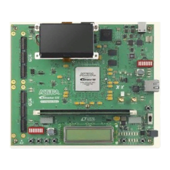
Stratix III Development Kit User Guide. Board Overview This section provides an overview of the Stratix III development board, including an annotated board image and component descriptions. May 2013 Altera Corporation Stratix III 3SL150 Development Board Reference Manual... - Page 10 D11, D12 (Port A) Green LEDs that indicate the RX and TX activity on the HSMC Ports A Channel activity LEDs or B. D2, D3 (Port B) Header Speaker header. Stratix III 3SL150 Development Board May 2013 Altera Corporation Reference Manual...
- Page 11 The P-SRAM devices connect to the MAX II device as well as the flash U4, U10 P-SRAM memory device. U17, U20 DDR2 SDRAM Two 16M × 8, 1.8-V core devices in 60-pin FBGA packages. May 2013 Altera Corporation Stratix III 3SL150 Development Board Reference Manual...
-
Page 12: Featured Fpga (U22)
Special Pins Oscillators and SMAs 1.8-V CMOS Three clock inputs, one output DDR2 DIMM 1.8-V SSTL 18 data strobe signal (DQS) pins DDR2 devices 1.8-V SSTL Four DQS pins Stratix III 3SL150 Development Board May 2013 Altera Corporation Reference Manual... - Page 13 Bank 5A Bank 2A USB, Misc DDR2 x 72 DIMM LCD, 1.8 V (136 pins) USER 7-SEG 2.5 V (35 pins) For additional information about Altera devices, go to www.altera.com/products/devices. May 2013 Altera Corporation Stratix III 3SL150 Development Board Reference Manual...
-
Page 14: Device Support
576 18 × 18 multipliers in FIR mode ■ I/O Resources This section lists specific I/O resources available with the EP3SL150F1152 device, which is from the L family of Stratix III devices. Stratix III 3SL150 Development Board May 2013 Altera Corporation Reference Manual... - Page 15 Bank 6A Bank 1A Bank 6B Bank 1B Bank 5C Bank 1C EP3SL340 Bank 5C Bank 2C Bank 5B Bank 2B Bank 2A Bank 5A Bank Name Number of I/Os May 2013 Altera Corporation Stratix III 3SL150 Development Board Reference Manual...
-
Page 16: Max Ii Cpld
Chapter 2: Board Components MAX II CPLD MAX II CPLD The board utilizes an Altera MAX II CPLD (U5) for the following purposes: Power-up configuration of the FPGA from flash memory ■ Embedded USB-Blaster core for USB-based configuration of the FPGA ■... - Page 17 U9 pin A8 and U4 pin 1.8 V FSM_A21 and P-SRAM bit 21 H6 and U10 pin H6 Address bus shared with flash 1.8 V U9 pin G1 FSM_A22 and P-SRAM bit 22 May 2013 Altera Corporation Stratix III 3SL150 Development Board Reference Manual...
- Page 18 Data bus shared with flash and 1.8 V U10 pin C6 FSM_D18 SRAM bit 18 Data bus shared with flash and 1.8 V U10 pin D5 FSM_D19 SRAM bit 19 Stratix III 3SL150 Development Board May 2013 Altera Corporation Reference Manual...
- Page 19 FPP configuration data bus bit 2 FPGA_DATA2 2.5 V — FPP configuration data bus bit 3 FPGA_DATA3 2.5 V — FPP configuration data bus bit 4 FPGA_DATA4 2.5 V — May 2013 Altera Corporation Stratix III 3SL150 Development Board Reference Manual...
- Page 20 Cypress/FTDI USB data bus bit 0 USB_PHY_FD0 2.5 V — pin 25 U12 pin 19 and U11 Cypress/FTDI USB data bus bit 1 USB_PHY_FD1 2.5 V — pin 24 Stratix III 3SL150 Development Board May 2013 Altera Corporation Reference Manual...
- Page 21 — U12 pin 35 USB_PA2_SLOE slave FIFOs. Cypress USB pin multiplexed for U12 pin 36 and U11 2.5 V — USB_PA3_WU2 I/O or alternate wake up signal pin 11 May 2013 Altera Corporation Stratix III 3SL150 Development Board Reference Manual...
- Page 22 — U19 pin 17 PMON_SYNC the power monitor multiplexer Power selection input 1.8 V — SW6 pin P1 PWR_SEL0 Power selection input 1.8 V — SW6 pin P2 PWR_SEL1 Stratix III 3SL150 Development Board May 2013 Altera Corporation Reference Manual...
- Page 23 1.8 V — U11 pin 10 USB_PWR_ENn 24 MHz clock input 1.8 V — Y4 pin 3 CLKIN_24 125 MHz clock input 1.8 V — Y1 pin 4 CLKIN_MAX_125 May 2013 Altera Corporation Stratix III 3SL150 Development Board Reference Manual...
- Page 24 MAX II component reference and manufacturing information. Table 2–6. MAX II Component Reference and Manufacturing Information Manufacturing Manufacturer Board Reference Description Manufacturer Part Number Website 256-pin device in a BGA package Altera Corporation EPM2210GF256C3N www.altera.com Stratix III 3SL150 Development Board May 2013 Altera Corporation Reference Manual...
-
Page 25: Configuration, Status, And Setup Elements
Board reference SW1 position 4 (SW1.4), labeled MAX_ENABLE must be in the 0 position for this feature to work properly. For more information about: ■ Advanced JTAG settings, refer to Table 2–7. May 2013 Altera Corporation Stratix III 3SL150 Development Board Reference Manual... - Page 26 (3) Board reference SW2.5 might need to be set to off (0) for the embedded USB-Blaster to program the Stratix III FPGA. (4) Requires external USB-Blaster or equivalent plugged into board reference J23 (PCB bottom). (5) “1” indicates the PFL is enabled and “0” indicates the PFL is disabled. Stratix III 3SL150 Development Board May 2013 Altera Corporation Reference Manual...
-
Page 27: Fpga Programming From Flash Memory
USB 2.0 interface and the Quartus II Programmer’s JTAG mode. The development kit implements the Altera PFL megafunction for flash programming. The PFL is a block of logic that is programmed into an Altera programmable logic device (FPGA or CPLD). The PFL functions as a utility for writing to a compatible flash device. -
Page 28: Board Specific Leds
Illuminates when transmit data is active from the HSMC. Driven by the Stratix III HSMC Port A TX device. HSMC Port A RX Illuminates when receive data is active from the HSMC. Driven by the Stratix III device. Stratix III 3SL150 Development Board May 2013 Altera Corporation Reference Manual... -
Page 29: Power Display
FPGA_BYPASS 0 = FPGA not in JTAG chain 1 = HSMC Port A in JTAG chain (only if installed) HSMA_BYPASS 0 = HSMC Port A not in JTAG chain May 2013 Altera Corporation Stratix III 3SL150 Development Board Reference Manual... -
Page 30: Max Ii Device Control Dip Switch
Table 2–13. MAX II Device Control DIP Switch Component Reference and Manufacturing Information Manufacturing Manufacturer Board Reference Description Manufacturer Part Number Website 8-position rocker DIP switch Grayhill Corporation 76SB08ST www.grayhill.com Stratix III 3SL150 Development Board May 2013 Altera Corporation Reference Manual... -
Page 31: System Reset And Configuration Switches
Upon first use, after configuring or powering up the board, make sure you initiate changes to the rotary switch (SW6) so that the measurement circuit can initiate a channel reading. Otherwise, the measurement might be reading a previous capture. May 2013 Altera Corporation Stratix III 3SL150 Development Board Reference Manual... -
Page 32: Pgm Config Select Rotary Switch
Stratix III FPGA design is loaded. The rotary switch has 16 positions but only the first eight are used. For information about the flash memory locations, refer to “Flash Memory” on page 2–63. Stratix III 3SL150 Development Board May 2013 Altera Corporation Reference Manual... -
Page 33: Clocking Circuitry
6-MHz USB PHY reference clock (FTDI device) ■ 24-MHz USB PHY reference clock (Cypress device) ■ 25-MHz Ethernet PHY reference clock ■ ■ SMA connectors for clocking input and output signals May 2013 Altera Corporation Stratix III 3SL150 Development Board Reference Manual... -
Page 34: Stratix Iii Fpga Clock Inputs
Bank 2C Bank 5C ENET_S_CLKN HSMB_CLK_IN_N2 CLK2N CLK9N 2.5 V HSMC 2.5 V Port B CLK3P CLK8P Bank 3C Bank 4C CLK3N CLK8N 1.8 V 1.8 V CLKIN_SMA SMA Input Stratix III 3SL150 Development Board May 2013 Altera Corporation Reference Manual... -
Page 35: Stratix Iii Fpga Clock Outputs
Lighthorse Technologies LTI-SASF546-P26-X1 www.rfconnector.com input/output 24-MHz crystal Abracon Corporation ABL-24.000MHZ-12 www.abracon.com 6-MHz crystal Abracon Corporation ABL-6.000MHZ-B2 www.abracon.com 25-MHz crystal oscillator ECS, Inc. ECS-3953C-250-B www.ecsxtal.com 24-MHz crystal oscillator Pletronics SM5545TEX-24.00M www.pletronics.com May 2013 Altera Corporation Stratix III 3SL150 Development Board Reference Manual... -
Page 36: General User Interfaces
0; when the switch is released, the device pin is set to a logic 1. There is no board-specific function for these four push-button switches. Stratix III 3SL150 Development Board May 2013 Altera Corporation Reference Manual... -
Page 37: User-Defined Dip Switches
User-defined DIP switch pin 4 1.8 V USER_DIPSW3 SW5 pin 5 User-defined DIP switch pin 5 1.8 V USER_DIPSW4 SW5 pin 6 User-defined DIP switch pin 6 1.8 V USER_DIPSW5 May 2013 Altera Corporation Stratix III 3SL150 Development Board Reference Manual... -
Page 38: User-Defined Leds
User-defined LED 1.8 V USER_LED2 User-defined LED 1.8 V USER_LED3 User-defined LED 1.8 V USER_LED4 User-defined LED 1.8 V USER_LED5 User-defined LED 1.8 V USER_LED6 User-defined LED 1.8 V USER_LED7 Stratix III 3SL150 Development Board May 2013 Altera Corporation Reference Manual... -
Page 39: Hsmc User-Defined Leds
Green LED, 1206, SMT, clear lens, D2, D3, D11, D12 Lumex, Inc. SML-LX1206GC-TR www.lumex.com 2.1 V 7-Segment Displays This section discusses the following two on-board displays: ■ User 7-segment display ■ Power 7-segment display May 2013 Altera Corporation Stratix III 3SL150 Development Board Reference Manual... -
Page 40: User 7-Segment Display
7-segment display component reference and manufacturing information. Table 2–30. 7-Segment Display Component Reference and Manufacturing Information Manufacturing Manufacturer Board Reference Description Manufacturer Part Number Website 7-segment, green LED display Lumex, Inc. LDQ-M2212R1 www.lumex.com Stratix III 3SL150 Development Board May 2013 Altera Corporation Reference Manual... -
Page 41: Power 7-Segment Display
LCD_DATA7 J22 pin 4 LCD data/command select 2.5 V LCD_D_Cn J22 pin 5 LCD write enable 2.5 V LCD_WEn J22 pin 6 LCD chip select 2.5 V AD12 LCD_CSn May 2013 Altera Corporation Stratix III 3SL150 Development Board Reference Manual... - Page 42 The particular model used does not have a backlight and the LCD drive pin is not connected. Figure 2–10. LCD Display Block Diagram Block Diagram 16 X 2, 1/16 Duty, 1/5 Bias DB[7:0] SEC 80 Controller Driver COM 16 Panel LED Backlight Stratix III 3SL150 Development Board May 2013 Altera Corporation Reference Manual...
-
Page 43: Graphics Lcd
LCD data bus bit 1 2.5 V AG32 OLED_DATA1 J24 pin 8 LCD data bus bit 2 2.5 V AB27 OLED_DATA2 J24 pin 9 LCD data bus bit 3 2.5 V AC32 OLED_DATA3 May 2013 Altera Corporation Stratix III 3SL150 Development Board Reference Manual... - Page 44 Optrex data sheet showing the control chip in the LCD module and illustrates the functional block diagram of the display driver. The control chip is from New Japan Radio Corporation, part number NJU6676. Stratix III 3SL150 Development Board May 2013 Altera Corporation Reference Manual...
- Page 45 Column Address Counter Column Address Register OSC1 Oscillator OSC2 Multiplexer Instruction Status Status Busy Flag Bus Holder Decoder Internal Bus Line Reset MPU Interface D5 to D0 (SI) (SCL) May 2013 Altera Corporation Stratix III 3SL150 Development Board Reference Manual...
-
Page 46: Speaker Header
Table 2–37. Speaker Header Component Reference and Manufacturing Information Manufacturing Manufacturer Board Reference Description Manufacturer Part Number Website Speaker header Samtec TSW-104-07-G-S www.samtec.com Stratix III 3SL150 Development Board May 2013 Altera Corporation Reference Manual... -
Page 47: Components And Interfaces
2.5-V and 1.1-V power rails and requires a 25-MHz reference clock driven from a dedicated oscillator. It interfaces to a HALO HFJ11-1G02E model RJ-45 with internal magnetics that can be used for driving copper lines with Ethernet traffic. May 2013 Altera Corporation Stratix III 3SL150 Development Board Reference Manual... - Page 48 U25 pin 93 GMII/ RGMII interface receive data bus bit 2 2.5 V AL33 ENET_RX_D2 U25 pin 91 GMII/ RGMII interface receive data bus bit 3 2.5 V AJ32 ENET_RX_D3 Stratix III 3SL150 Development Board May 2013 Altera Corporation Reference Manual...
-
Page 49: High-Speed Mezzanine Cards
Samtec ASP-122953-01. The HSMC interface also allows for JTAG, SMBus, clock outputs and inputs, as well as power for compatible HSMCs. The HSMC is an Altera-developed specification, which allows users to expand the functionality of the development board through the addition of daughter cards (HSMCs). - Page 50 Stratix III board uses a regular input pin due to lack of input clock resources. This means that clocks driven from the HSMC cannot be routed to a PLL. This limitation is true for both HSMC Port A and HSMC Port B. Stratix III 3SL150 Development Board May 2013 Altera Corporation Reference Manual...
- Page 51 J18 pin 68 LVDS RX or CMOS I/O bit 3 LVDS or 2.5 V HSMA_RX_N3 J18 pin 71 LVDS TX or CMOS I/O bit 4 LVDS or 2.5 V HSMA_TX_P4 May 2013 Altera Corporation Stratix III 3SL150 Development Board Reference Manual...
- Page 52 J18 pin 127 LVDS TX or CMOS I/O bit 12 LVDS or 2.5 V HSMA_TX_N12 J18 pin 128 LVDS RX or CMOS I/O bit 12 LVDS or 2.5 V HSMA_RX_N12 Stratix III 3SL150 Development Board May 2013 Altera Corporation Reference Manual...
- Page 53 Dedicated CMOS clock in 2.5 V HSMB_CLK_IN0 J8 pin 41 Dedicated CMOS I/O bit 0 2.5 V AB24 HSMB_D0 J8 pin 42 Dedicated CMOS I/O bit 1 2.5 V AB25 HSMB_D1 May 2013 Altera Corporation Stratix III 3SL150 Development Board Reference Manual...
- Page 54 HSMB_CLK_OUT_N1 J8 pin 98 LVDS or CMOS clock in LVDS or 2.5 V HSMB_CLK_IN_N1 J8 pin 101 LVDS TX or CMOS I/O bit 8 LVDS or 2.5 V HSMB_TX_P8 Stratix III 3SL150 Development Board May 2013 Altera Corporation Reference Manual...
- Page 55 LVDS or CMOS clock in LVDS HSMB_CLK_IN_P2 J8 pin 157 LVDS or CMOS clock out 2.5 V HSMB_CLK_OUT_N2 J8 pin 158 LVDS or CMOS clock in 2.5 V HSMB_CLK_IN_N2 May 2013 Altera Corporation Stratix III 3SL150 Development Board Reference Manual...
-
Page 56: On-Board Memory
AN 435: Using DDR and DDR2 SDRAM in Stratix III and Stratix IV Devices ■ AN 438: Constraining and Analyzing Timing for External Memory Interfaces in ■ Stratix III and Cyclone III Devices Stratix III 3SL150 Development Board May 2013 Altera Corporation Reference Manual... -
Page 57: Ddr2 Sdram Dimm
The data interface to the FPGA fabric runs at either one-half or one-quarter the ® physical layer data rate when using the Altera DDR2 MegaCore function, which equates to a doubling or quadrupling of the physical data bus width (144 bits or 288 bits, respectively). - Page 58 Data bit 32 SSTL-18 class I AE20 DDR2_DIMM_DQ32 J19 pin 81 Data bit 33 SSTL-18 class I AF21 DDR2_DIMM_DQ33 J19 pin 86 Data bit 34 SSTL-18 class I AP24 DDR2_DIMM_DQ34 Stratix III 3SL150 Development Board May 2013 Altera Corporation Reference Manual...
- Page 59 Data bit 71 SSTL-18 class I AK24 DDR2_DIMM_DQ71 J19 pin 6 Data strobe bit 0 SSTL-18 class I AL11 DDR2_DIMM_DQS_N0 J19 pin 15 Data strobe bit 1 SSTL-18 class I DDR2_DIMM_DQS_N1 May 2013 Altera Corporation Stratix III 3SL150 Development Board Reference Manual...
- Page 60 J19 pin 120 Presence-detect clock SSTL-18 class I AN15 DDR2_DIMM_SCL J19 pin 119 Presence-detect data SSTL-18 class I AK19 DDR2_DIMM_SDA J19 pin 73 Write enable SSTL-18 class I AJ19 DDR2_DIMM_WEn Stratix III 3SL150 Development Board May 2013 Altera Corporation Reference Manual...
-
Page 61: Ddr2 Sdram Devices
Data bit 2 SSTL-18 class I U22-K28 DDR2_DEVA_DQ2 U17 pin D3 Data bit 3 SSTL-18 class I U22-J29 DDR2_DEVA_DQ3 U17 pin D1 Data bit 4 SSTL-18 class I U22-H32 DDR2_DEVA_DQ4 May 2013 Altera Corporation Stratix III 3SL150 Development Board Reference Manual... - Page 62 Address bit 9 SSTL-18 class I U22-V31 DDR2_DEVB_A9 U20 pin H2 Address bit 10 SSTL-18 class I U22-P34 DDR2_DEVB_A10 U20 pin K7 Address bit 11 SSTL-18 class I U22-T29 DDR2_DEVB_A11 Stratix III 3SL150 Development Board May 2013 Altera Corporation Reference Manual...
-
Page 63: Qdrii+ Sram
350 MHz. Burst-of-2 devices have a DDR address bus allowing for different read and write addresses on every clock (two data words per clock). Burst-of-4 devices have higher data rates due to the longer sequential addressing. May 2013 Altera Corporation Stratix III 3SL150 Development Board Reference Manual... - Page 64 1.5-V HSTL class I QDRII_D9 U15 pin C3 Write data bit 10 1.5-V HSTL class I QDRII_D10 U15 pin D2 Write data bit 11 1.5-V HSTL class I QDRII_D11 Stratix III 3SL150 Development Board May 2013 Altera Corporation Reference Manual...
- Page 65 Valid output indicator 1.5-V HSTL class I QDRII_QVLD U15 pin A8 Read port select 1.5-V HSTL class I QDRII_RPSn U15 pin A4 Write port select 1.5-V HSTL class I QDRII_WPSn May 2013 Altera Corporation Stratix III 3SL150 Development Board Reference Manual...
-
Page 66: P-Sram
The P-SRAM devices are part of a shared bus with connectivity to the MAX II CPLD as well as the flash memory, which is called the FSM bus. All three devices use 1.8-V CMOS signaling. Altera recommends using the 5-Ω OCT setting on the FPGA and the one-half drive setting on the SRAM. - Page 67 1.8 V FSM_D8 P-SRAM bit 8 pin F4 Data bus shared with flash and U5 pin T4 and U9 U4 pin C1 1.8 V FSM_D9 P-SRAM bit 9 pin F5 May 2013 Altera Corporation Stratix III 3SL150 Development Board Reference Manual...
- Page 68 U10 pin F2 1.8 V U5 pin D14 FSM_D29 P-SRAM bit 29 Data bus shared with flash and U10 pin F1 1.8 V U5 pin E12 FSM_D30 P-SRAM bit 30 Stratix III 3SL150 Development Board May 2013 Altera Corporation Reference Manual...
- Page 69 Latency 4 (Burst Length: 8) Data Out Latency 4 (Burst Length: 8) Data In Variable Latency - A18[1] Latency 2 (Burst Length: 8) Data In/Out Latency 2 (Burst Length: 8) Data Out May 2013 Altera Corporation Stratix III 3SL150 Development Board Reference Manual...
- Page 70 Samsung device read and write access waveforms. Figure 2–18. SRAM Read Timing Waveforms ADDR UB, LB Data Out WAIT Figure 2–19. SRAM Write Timing Waveforms ADDR UB, LB Data In WAIT Stratix III 3SL150 Development Board May 2013 Altera Corporation Reference Manual...
-
Page 71: Flash Memory
Address bus shared with U5 pin P10 and U4 pin H5 and U9 pin A5 1.8 V FSM_A12 flash and P-SRAM bit 12 U10 pin H5 and U5 pin P10 May 2013 Altera Corporation Stratix III 3SL150 Development Board Reference Manual... - Page 72 U5 pin N6 and U4 pin B1 FSM_D8 flash and P-SRAM bit 8 Data bus shared with U9 pin E3 1.8 V U5 pin T4 and U4 pin C1 FSM_D9 flash and P-SRAM bit 9 Stratix III 3SL150 Development Board May 2013 Altera Corporation Reference Manual...
- Page 73 FPGA design. Table 2–56. Flash Memory Map (Part 1 of 2) Name Address PFL option bits 0x03FE.0000 Ethernet option bits 0x03FC.0000 0x03FB.FFFF User space (10 MBytes) 0x0350.0000 May 2013 Altera Corporation Stratix III 3SL150 Development Board Reference Manual...
- Page 74 Table 2–58. Flash Memory Device Component Reference and Manufacturing Information Manufacturing Manufacturer Board Reference Description Manufacturer Part Number Website 512 Mbit, 1.7 to 2.0 V core, 64-pin BGA Intel Corporation PC48F4400P0VB00 www.intel.com Stratix III 3SL150 Development Board May 2013 Altera Corporation Reference Manual...
-
Page 75: Power Supply
Partial Plane QDRII VDD VREF_QDRII V IN Linear VTT _ QDRII (TPS5100) Power Net 0 . 9 V / 0 . 75 V VDDQ_QDRII V VLDOIN QDR II Termination Resistors May 2013 Altera Corporation Stratix III 3SL150 Development Board Reference Manual... -
Page 76: Power Measurement
FPGA I/O power bank 2 2.5V_B2 VCCIO2C VCCIO4A, VCCIO5A, FPGA I/O power banks 4a, 5, 6 2.5V_B4A_B5_B6 VCCIO5C, VCCIO6A, VCCIO6C VCCIO7A, FPGA I/O power bank 7 1.5V_1.8V_B7 VCCIO7B, VCCIO7C Stratix III 3SL150 Development Board May 2013 Altera Corporation Reference Manual... -
Page 77: Security Key And Battery Backup
Additionally, the V power CCBAT input has a jumper to allow the VCCBAT pin to be tied directly to GND when the battery is removed for supporting the non-volatile key mode. May 2013 Altera Corporation Stratix III 3SL150 Development Board Reference Manual... -
Page 78: Statement Of China-Rohs Compliance
(2) X* indicates that the concentration of the hazardous substance of at least one of all homogeneous materials in the parts is above the relevant threshold of the SJ/T11363-2006 standard, but it is exempted by EU RoHS. Stratix III 3SL150 Development Board May 2013 Altera Corporation... -
Page 79: Additional Information
Additional Information This chapter provides additional information about the document and Altera. Document Revision History The following table lists the revision history for this document. Date Version Changes Updated the MAX II pin assignment for FSM_A9 signal in Table 2–5. -
Page 80: How To Contact Altera
(software licensing) Email authorization@altera.com Note to Table: (1) You can also contact your local Altera sales office or sales representative. Typographic Conventions The following table shows the typographic conventions this document uses. Visual Cue Meaning Indicate command names, dialog box titles, dialog box options, and other GUI Bold Type with Initial Capital labels. - Page 81 Email Subscription Management Center page of the Altera website, where you can sign up to receive update notifications for Altera documents. The feedback icon allows you to submit feedback to Altera about the document. Methods for collecting feedback vary as appropriate for each document.
- Page 82 Info–4 Additional Information Typographic Conventions Stratix III 3SL150 Development Board May 2013 Altera Corporation Reference Manual...
Need help?
Do you have a question about the Stratix III 3SL150 and is the answer not in the manual?
Questions and answers