Table of Contents
Advertisement
Quick Links
Revision history
Rev
Date
v.1
20220419
UM11758
UJA1169A evaluation boards
Rev. 1 — 19 April 2022
Description
Initial version
IMPORTANT NOTICE
For engineering development or evaluation purposes only
NXP provides the product under the following conditions:
This evaluation kit is for use of ENGINEERING DEVELOPMENT OR
EVALUATION PURPOSES ONLY. It is provided as a sample IC pre-
soldered to a printed-circuit board to make it easier to access inputs,
outputs and supply terminals. This evaluation board may be used with any
development system or other source of I/O signals by connecting it to the
host MCU computer board via off-the-shelf cables. This evaluation board
is not a Reference Design and is not intended to represent a final design
recommendation for any particular application. Final device in an application
heavily depends on proper printed-circuit board layout and heat sinking
design as well as attention to supply filtering, transient suppression, and I/O
signal quality.
The product provided may not be complete in terms of required design,
marketing, and or manufacturing related protective considerations, including
product safety measures typically found in the end device incorporating the
product. Due to the open construction of the product, it is the responsibility of
the user to take all appropriate precautions for electric discharge. In order to
minimize risks associated with the customers' applications, adequate design
and operating safeguards must be provided by the customer to minimize
inherent or procedural hazards. For any safety concerns, contact NXP sales
and technical support services.
User manual
Advertisement
Table of Contents

Related Manuals for NXP Semiconductors UJA1169A


Summary of Contents for NXP Semiconductors UJA1169A
- Page 1 UM11758 UJA1169A evaluation boards Rev. 1 — 19 April 2022 User manual Revision history Date Description 20220419 Initial version IMPORTANT NOTICE For engineering development or evaluation purposes only NXP provides the product under the following conditions: This evaluation kit is for use of ENGINEERING DEVELOPMENT OR EVALUATION PURPOSES ONLY.
-
Page 2: Introduction
UJA1169A evaluation boards Introduction This document is the user guide for the UJA1169A evaluation boards. It is intended for engineers involved in the evaluation, design, implementation and validation of the UJA1169A product family. This guide discusses power supply requirements and the MCU and CAN bus interfaces, and describes how to connect the boards into an ECU/CAN network. -
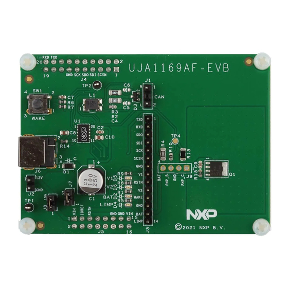
Page 3: Overview Of Boards
Top and bottom views of the UJA1169AXF-EVB board are illustrated in Figure 1. Unless otherwise stated, the information in this section applies to all UJA1169A evaluation boards. Board dimensions are 58.5 mm × 81.1 mm. Only components needed to support basic UJA1169A functionality are included. -
Page 4: Ground Connections
UM11758 NXP Semiconductors UJA1169A evaluation boards 2.1 Ground connections All ground pins are connected to the ground plane. Table 2. Ground connections Ground connections J2-02 J3-07/12 J4-13 J5-11/13 J6-02/03 J9-02 2.2 Power supply connections 2.2.1 Battery connections An external power supply must be connected to either power jack J6 or 2-pin header J2,... -
Page 5: V1/Pnp Connections
J9-04: connected indirectly via R4, 0 Ω to emitter of the onboard PNP transistor The internal V1 voltage regulator on the UJA1169A can deliver up to 250 mA without the need for an external PNP transistor. However, if critical thermal requirements need to be satisfied, it is possible to connect one or more external PNP transistors to share the total V1 load current, and therefore also share the thermal dissipation. -
Page 6: Uja1169A With One Pnp
PNP delivers additional supply current to the application. Detailed information on the functionality and operation of the UJA1169A can be found in the data sheet and application hints (see Section 2.2.2.1 UJA1169A with one PNP... -
Page 7: Uja1169A Without An External Pnp
UM11758 NXP Semiconductors UJA1169A evaluation boards 2.2.2.2 UJA1169A without an external PNP As already discussed, the UJA1169Ax-EVB can operate using only the V1 regulator in applications where thermal considerations are not critical. For this option, resistors R4 and R10 must be removed, as illustrated in... - Page 8 UM11758 NXP Semiconductors UJA1169A evaluation boards additional PNP(s) 10 Ω 10 Ω 10 Ω 10 nF 10 nF 10 nF 100 k 100 k 100 k 0 Ω VEXCTRL (p15) PNP_B VEXCC (p6) PNP_C UJA1169A 1.6 Ω V1 (p5) 6.8 F...
-
Page 9: V2/Vext Connection
NXP Semiconductors UJA1169A evaluation boards 2.2.3 V2/VEXT connection UJA1169A devices contain a second on-chip 5 V regulator. On the UJA1169ATK, UJA1169ATK/F, UJA1169ATK/3 and UJA1169ATK/F/3 variants, this regulator (V2) supplies the internal CAN transceiver and/or additional onboard hardware. On the UJA1169ATK/X and UJA1169ATK/X/F variants, the second regulator (VEXT) is intended to supply off-board components such as sensors. -
Page 10: Can Communication Circuitry
ESD protection diodes aaa-045540 Figure 10. CAN bus interface circuitry (relevant for the entire UJA1169A-EVB family) UM11758 All information provided in this document is subject to legal disclaimers. © NXP B.V. 2022. All rights reserved. User manual Rev. 1 — 19 April 2022... -
Page 11: Wake-Up Options
UJA1169A register map (as described in the UJA1169A data sheet [1]). Regulator V1 on the UJA1169A is intended to supply the MCU. V1 is off in Sleep mode and switches on automatically when a wake-up event is detected. -
Page 12: Limp Output
UM11758 NXP Semiconductors UJA1169A evaluation boards 2.5 LIMP output The LIMP pin can be accessed on top-side connector J3. It is targeted at applications that need a ‘limp home’ feature in the event of serious ECU failure. LIMP is an open-drain low-side output. -
Page 13: Mcu Interface
MCU. The remaining four pins are used for SPI communication with the MCU. A bidirectional reset signal (connected to the RSTN pin on the UJA1169A) is also accessible on J3 and J5. Table 9. TXD, RXD and SPI connections... -
Page 14: Reset Connection
A 10 kΩ pull-up resistor is connected between RSTN and V1 on the evaluation boards. A reset event is triggered by a LOW level on RSTN. Details of reset functionality can be found in the UJA1169A data sheet and application hints [2]. -
Page 15: Connecting The Uja1169Ax-Evb Into A Can Network
Once the above steps have been completed, the ECU/EVB can be powered up using an external battery supply. The UJA1169A starts up in Forced Normal mode (if MTP is not configured) or Standby mode (if MTP configured), awaiting commands from the MCU via the SPI interface. -
Page 16: Schematic Diagrams
UM11758 NXP Semiconductors UJA1169A evaluation boards Schematic diagrams LAYOUT NOTE: PLACE R10, R13 CLOSE TO J9 12 V PNP_C SILK=PNP_C SILK=GND LAYOUT NOTE: PLACE C9 CLOSE TO Q1 SILK=12 V 0.01 µF PNP_B SILK=PNP_B SILK=GND SILK=BAT PHPT61003PY HDR_1X2 PNP_E RHDR_1X4 (1) - Page 17 UM11758 NXP Semiconductors UJA1169A evaluation boards LAYOUT NOTE: PLACE R10, R13 CLOSE TO J9 12 V PNP_C SILK=PNP_C SILK=GND LAYOUT NOTE: PLACE C9 CLOSE TO Q1 SILK=12 V 0.01 µF PNP_B SILK=PNP_B SILK=GND SILK=BAT PHPT61003PY HDR_1X2 PNP_E RHDR_1X4 (1) CON PWR 3...
- Page 18 UM11758 NXP Semiconductors UJA1169A evaluation boards LAYOUT NOTE: PLACE R10, R13 CLOSE TO J9 12 V PNP_C SILK=PNP_C SILK=GND LAYOUT NOTE: PLACE C9 CLOSE TO Q1 SILK=12 V 0.01 µF PNP_B SILK=PNP_B SILK=GND SILK=BAT PHPT61003PY HDR_1X2 PNP_E RHDR_1X4 (1) CON PWR 3...
-
Page 19: Bills Of Materials
UM11758 NXP Semiconductors UJA1169A evaluation boards Bills of Materials Table 11. Bill of Materials - UJA1169AF-EVB NXP does not assume liability, endorse, or warrant components from external manufacturers referenced in circuit drawings or tables. While NXP offers component recommendations in this configuration, it is the responsibility of the customer to validate their application. - Page 20 UM11758 NXP Semiconductors UJA1169A evaluation boards Table 12. Bill of Materials - UJA1169AF3-EVB NXP does not assume liability, endorse, or warrant components from external manufacturers referenced in circuit drawings or tables. While NXP offers component recommendations in this configuration, it is the responsibility of the customer to validate their application.
- Page 21 UM11758 NXP Semiconductors UJA1169A evaluation boards Table 13. Bill of Materials - UJA1169AXF-EVB NXP does not assume liability, endorse, or warrant components from external manufacturers referenced in circuit drawings or tables. While NXP offers component recommendations in this configuration, it is the responsibility of the customer to validate their application.
-
Page 22: Flexgui: Interactive Register Control Via Usb
Figure 19. Using FlexGUI with S32K144EVB as USB/SPI interface 6.1 FlexGUI software package overview The FlexGUI SW package for the UJA1169A evaluation boards can be downloaded from www.nxp.com. It includes: • the flexGUI PC installer (see also Section 6.3) - Page 23 UM11758 NXP Semiconductors UJA1169A evaluation boards Figure 20. S32K144EVB jumper settings for firmware programming Figure 21. PC connection for firmware programming Figure 22. Copying the firmware file to the EVB-S32K144 drive UM11758 All information provided in this document is subject to legal disclaimers.
-
Page 24: Hw Setup For Flexgui Operation
UM11758 NXP Semiconductors UJA1169A evaluation boards 6.2.2 HW setup for FlexGUI operation The watchdog in the SBC must be off while the FlexGUI is running. The watchdog is always off in Forced Normal mode and off by default in Software Development mode (a... -
Page 25: Installing The Flexgui On A Pc
NXP Semiconductors UJA1169A evaluation boards Figure 24. UJA119A-EVB/S32K144EVB supply and data line interconnections A 12 V power supply must be connected to header J2 or to jack J6 on the UJA1169A- EVB (see also Figure 19). It supplies the BAT pin of the SBC via a polarity protection diode. - Page 26 UM11758 NXP Semiconductors UJA1169A evaluation boards a. Windows Start menu b. Desktop shortcut Figure 25. FlexGUI start options During start-up, the FlexGUI launch window (Figure 26) displays a list of the evaluation boards covered by this FlexGUI installation. Select the appropriate board and click OK. A temporary pop-up window indicates the...
- Page 27 UM11758 NXP Semiconductors UJA1169A evaluation boards Figure 27. Window displayed during start-up Figure 28. FlexGUI start-up window; boards not yet connected UM11758 All information provided in this document is subject to legal disclaimers. © NXP B.V. 2022. All rights reserved. User manual Rev.
-
Page 28: Establishing A Connection Between The Flexgui And The Hardware
UM11758 NXP Semiconductors UJA1169A evaluation boards 6.4.2 Establishing a connection between the FlexGUI and the hardware To establish a connection between the FlexGUI and the hardware, a battery supply must first be provided for the UJA1169Ax-EVB (see Figure 19) before connecting the microcontroller board to the PC using a USB cable. -
Page 29: Spi Speed Selection
UM11758 NXP Semiconductors UJA1169A evaluation boards 6.4.3 SPI speed selection The SPI speed (frequency) can be specified in the lower-left section of the FlexGUI window (if that section of the window is not visible, click the slider symbol under the 'File' menu). - Page 30 UM11758 NXP Semiconductors UJA1169A evaluation boards Figure 31. Register map tab The registers are divided into groups. A register group can be selected in the left column. If option Tree View is selected, a single register may be selected (Tree View is selected via the FlexGUI pop up window accessed under File/Settings;...
- Page 31 UM11758 NXP Semiconductors UJA1169A evaluation boards The contents of the selected register, or register group, is displayed in the main window. Register data can be edited in the top row in preparation for writing to the register. When option Use Register Init Value is selected, the editor is initialized with the default values...
- Page 32 UM11758 NXP Semiconductors UJA1169A evaluation boards Figure 34. Register map with option 'Uniform Buttons' not selected. If there are more registers in a group than can be displayed on-screen, the registers are distributed over two or more pages and the active page can be selected at the bottom of the main window.
- Page 33 UM11758 NXP Semiconductors UJA1169A evaluation boards Multiple registers can be selected using the check boxes to the left of the register names. The selected registers will be included in later multi-registers operations. Four associated buttons are provided: • Write and read operations can be triggered with the Write and Read buttons.
-
Page 34: Working With The Script Editor
UM11758 NXP Semiconductors UJA1169A evaluation boards 6.4.6 Working with the script editor Selecting tab 'Script editor' opens a tool for creating, executing, loading and saving command sequences ('scripts') used for reading from or writing to registers. RGB LED settings (see Section 6.4.4) can also be included in such scripts. -
Page 35: Logging Read And Write Operations
UM11758 NXP Semiconductors UJA1169A evaluation boards Example script using all available commands: // This is an example script for UJA1169AXF-EVB // For UJA1169AF-EVB/UJA1169AF3-EVB replace "UJA1169AXF" with applicable device name // Do not run this script with the auto-repeat option, because the script includes a PAUSE command... - Page 36 UM11758 NXP Semiconductors UJA1169A evaluation boards Figure 37. Logging options Figure 38. FlexGUI 'FINEST' detail level selected for log window If the log window is not displayed, click on the slider symbol under the 'File' menu. UM11758 All information provided in this document is subject to legal disclaimers.
-
Page 37: Restrictions On Using Sbc In Sleep Mode
UM11758 NXP Semiconductors UJA1169A evaluation boards 6.4.8 Restrictions on using SBC in Sleep mode After executing a Sleep mode command successfully, the SBC turns off the output on V1 supplying the microcontroller. As a result, the connection between the GUI and the SBC will be lost after a short delay. -
Page 38: References
UM11758 NXP Semiconductors UJA1169A evaluation boards References UJA1169A data sheet — Mini high-speed CAN system basis chip: https://www.nxp.com/docs/en/data-sheet/UJA1169A.pdf AH1902 application — Mini high speed CAN system basis chips UJA116xA, available from NXP hints Semiconductors UM11758 All information provided in this document is subject to legal disclaimers. -
Page 39: Table Of Contents
2.2.1 Battery connections ........... 4 2.2.2 V1/PNP connections ..........5 2.2.2.1 UJA1169A with one PNP ........6 2.2.2.2 UJA1169A without an external PNP ....7 2.2.2.3 UJA1169Ax-EVB with multiple external PNPs ..............7 2.2.3 V2/VEXT connection ..........9 CAN communication circuitry ......10 Wake-up options ..........11 LIMP output .............
Need help?
Do you have a question about the UJA1169A and is the answer not in the manual?
Questions and answers