Table of Contents
Advertisement
Quick Links
UM11565
NAFExx388 evaluation board
Rev. 1 — 29 March 2023
Document information
Information
Keywords
Abstract
Content
SPI-bus, NAFE11388, NAFE71388, NAFE13388, NAFE73388 (Future release) analog front-end,
ADC, RTD, TC, HVDD, HVSS
The NAFExx388 evaluation board is easy to test and design for the NAFE11388, NAFE71388,
NAFE13388, and NAFE73388
analog input analog front-end (AFE) that meets high-precision measurement requirements. The
device is composed of a low-leakage, high-voltage multiplexer, low-offset drift buffers, a low noise
and drift PGA, a precision 24-bit sigma-delta analog-to-digital converter (ADC), low-drift voltage
reference. This evaluation board, along with the LPC54628 MCU board, provide an easy-to-use
evaluation platform.
1
which is a highly configurable, industrial-grade multichannel
User manual
Advertisement
Table of Contents

Related Manuals for NXP Semiconductors UM11565


Summary of Contents for NXP Semiconductors UM11565
- Page 1 UM11565 NAFExx388 evaluation board Rev. 1 — 29 March 2023 User manual Document information Information Content Keywords SPI-bus, NAFE11388, NAFE71388, NAFE13388, NAFE73388 (Future release) analog front-end, ADC, RTD, TC, HVDD, HVSS Abstract The NAFExx388 evaluation board is easy to test and design for the NAFE11388, NAFE71388,...
- Page 2 UM11565 NXP Semiconductors NAFExx388 evaluation board Table 1. Date Description 20230329 Initial release UM11565 All information provided in this document is subject to legal disclaimers. © 2023 NXP B.V. All rights reserved. User manual Rev. 1 — 29 March 2023...
- Page 3 UM11565 NXP Semiconductors NAFExx388 evaluation board IMPORTANT NOTICE For engineering development or evaluation purposes only NXP provides the product under the following conditions: This evaluation kit is for use of ENGINEERING DEVELOPMENT OR EVALUATION PURPOSES ONLY. It is provided as a sample IC pre-soldered to a printed-circuit board to make it easier to access inputs, outputs and supply terminals.
-
Page 4: Introduction
UM11565 NXP Semiconductors NAFExx388 evaluation board 1 Introduction The NAFExx388 evaluation board features a highly configurable, industrial-grade, multichannel AI-AFE family of parts (11388, 13388, etc. …) that meets high-precision measurement requirements. The device is composed of a low-leakage, high-voltage multiplexer, low-offset drift buffers, a low noise and drift PGA, a precision 24-bit sigma-delta analog-to-digital converter (ADC), and low-drift voltage reference. -
Page 5: Finding Kit Resources And Information On The Nxp Website
NXP Semiconductors NAFExx388 evaluation board 2 Finding kit resources and information on the NXP website NXP Semiconductors provides online resources for evaluation board and its supported device(s) on http:// www.nxp.com. The information page for NAFExx388-EVB evaluation board is at http://www.nxp.com/NAFExx388-EVB. The information page provides overview information, documentation, software and tools, parametrics, ordering information and a Getting Started tab. -
Page 6: Getting Ready
UM11565 NXP Semiconductors NAFExx388 evaluation board 3 Getting ready Working with the NAFExx388-EVB requires the kit contents, additional hardware, and a Windows PC workstation with installed software. 3.1 Kit contents • Assembled and tested evaluation board in an antistatic bag •... -
Page 7: Getting To Know The Hardware
UM11565 NXP Semiconductors NAFExx388 evaluation board 4 Getting to know the hardware 4.1 Board features Table 2. NAFExx388 evaluation board main components Device Description Location NAFExx388 Eight-input SW configurable AI-AFE MAX13256ATB Transformer driver TGMR-511V6LF Transformer Si8641BC-B-IS1 Quad-channel digital isolators Si8642BC-B-IS1 Quad-channel digital isolators... -
Page 8: Configuring The Hardware
UM11565 NXP Semiconductors NAFExx388 evaluation board 5 Configuring the hardware The NAFExx388 evaluation kit includes the NAFExx388 evaluation board, an OM13098 (LPC54628) evaluation board, and a USB cable. To set up the hardware, do the following: 1. Firmly connect the NAFExx388 (AFE) evaluation board to the LPC54628 (microcontroller) evaluation board using the Arduino connectors. - Page 9 UM11565 NXP Semiconductors NAFExx388 evaluation board Figure 2. Test setup showing connectivity between computer and evaluation system UM11565 All information provided in this document is subject to legal disclaimers. © 2023 NXP B.V. All rights reserved. User manual Rev. 1 — 29 March 2023...
-
Page 10: Schematic, Board Layout, Bill Of Materials
UM11565 NXP Semiconductors NAFExx388 evaluation board 6 Schematic, board layout, bill of materials REFCAL_H ADX_REFCAL_H REFCAL_H 1 kΩ 10 nF REFCAL_L ADX_REFCAL_L REFCAL_L 1 kΩ 10 nF AUX_3V3 DUT_-15V0 AI4- ADC AI4- AI4- 2.4 kΩ C244 Diode TVS BI-DR 4.7 µF... - Page 11 UM11565 NXP Semiconductors NAFExx388 evaluation board DUT POWER SUPPLIES MCU POWER SUPPLIES Banana Jack Red 694103303002 Banana Jack Red Banana Jack Red Banana Jack Red Banana Jack Red 24 V 3V3_D EXT_3V3 EXT_15V0 EXT_-15V0 R185 R183 5.11 Ω 5.11 Ω...
- Page 12 UM11565 NXP Semiconductors NAFExx388 evaluation board Install jumper if all four DACs be reset at the same time. LPC54628 ARDUINO INTERFACE HEADERS P4_6-FC9_SSELn1 P0_16-ADC0IN4 P3_24-FC2_SCLX P1_18-CAN1_RD ADC_nDRDY P3_16-GPIO_SPI_CS2 P0_31-ADC0IN5 P3_23-FC2_SCAX P1_17-CAN1_TD 47 Ω ADC_nINT P1_0-ADC0IN6 JS19 on LPC54628 connected to pin 5...
- Page 13 UM11565 NXP Semiconductors NAFExx388 evaluation board Figure 6. Component and jumpers locations The schematic, board layout and bill of materials for the NAFExx388 evaluation board are available at http:// www.nxp.com/NAFExx388-EVB. UM11565 All information provided in this document is subject to legal disclaimers.
-
Page 14: Tool Interface
UM11565 NXP Semiconductors NAFExx388 evaluation board 7 Tool interface 7.1 GUI installation • Right click on the executable (SetupNAFExx388_x.x.x), run as administrator, and follow the prompts to install the application. • Click the Windows start button on bottom left and find the NAFExx388_EVB GUI application. -
Page 15: Connectivity Check
UM11565 NXP Semiconductors NAFExx388 evaluation board Figure 8. MCU board firmware update 7.3 Connectivity check Click the NAFExx388_EVB GUI application to open the GUI. If there isn’t connection with the MCU or the evaluation board, the message on the left top of GUI will be the following: The label "Disconnected"... -
Page 16: Using The Tool
UM11565 NXP Semiconductors NAFExx388 evaluation board The NAFExx388 GUI is a smart GUI that caters to the full part family. The block diagram is updated based on the part read back, that is, the VIEX block shows up for NAFEx3388 devices only. -
Page 17: Data-Rate Selection
UM11565 NXP Semiconductors NAFExx388 evaluation board b. Click the Continuous Reading button and wait for the dialog box to pick the folder to create a .csv conversion results file on the hard drive with the number of samples requested. 7.4.3 Data-rate selection The AI-AFE provides a flexible ADC configuration that enables the user to configure Settling mode, digital SINC filter, and data rate. -
Page 18: Application Test Cases
UM11565 NXP Semiconductors NAFExx388 evaluation board Table 6. Calibration coefficients table CHANNEL POINTER/ GAIN OFFSET POINTER PGA SETTING OFFSET COEFF GAIN COEFF PGA0: Channel gain = 0.2 V/V SINGLE ENDED AIxP 0x0000FD 0x7EC2EA PGA1: Channel gain = 0.4 V/V SINGLE ENDED AIxP... - Page 19 UM11565 NXP Semiconductors NAFExx388 evaluation board 2. Select input channels from the MUX dropdown menu (HV_INP, HV_INV). Figure 10. Input channels 3. Select PGA, SINC FILTER, ADC SETTING MODE, ADC DATA RATE, CHANNEL PROGRAM DELAY and CALIBRATION COEFFICIENT settings in the dropdown menus.
-
Page 20: Single-Channel Continuous Reading (Sccr) Example
UM11565 NXP Semiconductors NAFExx388 evaluation board Figure 11. Dropdown menus 4. Click the Single Reading button to read a single-channel voltage value in the Reading Result box. Figure 12. Single Reading button 7.5.2 Single-Channel Continuous Reading (SCCR) example 1. Follow steps 1 through 3 described in Section 7.5.1. - Page 21 UM11565 NXP Semiconductors NAFExx388 evaluation board Figure 13. Number of samples 3. Click the Continuous Reading button to read in Single Channel multiple-voltage values, and export data in the .csv file. Figure 14. Continuous Reading button 4. Open the .csv file to see number of voltage values.
-
Page 22: Multi-Channel Reading (Mcr) Example
UM11565 NXP Semiconductors NAFExx388 evaluation board Figure 15. Voltage values 7.5.3 Multi-Channel Reading (MCR) example 1. Select multiple channels by clicking in the Enable checkboxes. UM11565 All information provided in this document is subject to legal disclaimers. © 2023 NXP B.V. All rights reserved. - Page 23 UM11565 NXP Semiconductors NAFExx388 evaluation board Figure 16. Select channels 2. Select the enabled channel configuration (channel #0-16 config) one by one in the AFE Config dropdown menu. Figure 17. Channel configuration 3. Select input channels from the MUX dropdown menu (HV_INP, HV_INV).
- Page 24 UM11565 NXP Semiconductors NAFExx388 evaluation board Figure 18. MUX dropdown menu 4. Select PGA, SINC FILTER, ADC SETTING MODE, ADC DATA RATE, CHANNEL PROGRAM DELAY and CALIBRATION COEFFICIENT settings for each channel configuration in the dropdown menus. UM11565 All information provided in this document is subject to legal disclaimers.
- Page 25 UM11565 NXP Semiconductors NAFExx388 evaluation board Figure 19. Select settings 5. Click the Multi-Reading button to read the voltage value in multiple channels in the Reading Result boxes. UM11565 All information provided in this document is subject to legal disclaimers. © 2023 NXP B.V. All rights reserved.
-
Page 26: Multi-Channel Continuous Reading (Mccr) Example
UM11565 NXP Semiconductors NAFExx388 evaluation board Figure 20. Multi-Reading button 7.5.4 Multi-Channel Continuous Reading (MCCR) example 1. Follow steps 1 through 3 as described in Section 7.5.3. 2. Key in the number in the Number of loops box. UM11565 All information provided in this document is subject to legal disclaimers. - Page 27 UM11565 NXP Semiconductors NAFExx388 evaluation board Figure 21. Number of loops 3. Click the Continuous Reading button to read the voltage values of multiple channels and export data in the .csv file. Figure 22. Continuous Reading 4. Open the .csv file to see the number of voltage values.
-
Page 28: Save And Load Configuration File
UM11565 NXP Semiconductors NAFExx388 evaluation board Figure 23. Voltage values 7.5.5 Save and load configuration file The NAFExx388 GUI provides user-friendly save-and-load configuration file function, which allows the user to save current AFE channel #0-16 configurations, GPIO configuration, SCCR number of samples, MCCR- enabled channel, and MCCR number of loops in an .acs (AFE configuration settings) file. -
Page 29: Load Configuration File
UM11565 NXP Semiconductors NAFExx388 evaluation board Figure 25. Example save file 7.5.5.2 Load configuration file 1. To launch the NAFExx388 GUI, select Open AFE configuration in the File tab. Figure 26. Launch the GUI 2. Open the saved .acs file to load all configuration settings and proceed, repeating the previous measurement or modifying some settings for a new measurement. -
Page 30: Fast Fourier Transform (Fft) Spectrum Analysis
UM11565 NXP Semiconductors NAFExx388 evaluation board Figure 27. Open example save file 7.5.6 Fast Fourier transform (FFT) spectrum analysis It is important the frequency of the source generator and the AI-AFE clock are coherent to perform an accurate spectrum analysis. Two conditions should be satisfied to have a coherent measurement: 1. -
Page 31: Test Conditions For Coherent Measurement
UM11565 NXP Semiconductors NAFExx388 evaluation board 7.5.6.2 Test conditions for coherent measurement Sample Number = 8192. Master clock (MCLK) = 18.432 MHz (provided by AWG, CH-2) Input Frequency = 1001.953125 Hz (provided by AWG, CH-1) Figure 29. Input frequency Note: If the ADC is set in Normal Settling mode, it is recommended to capture five more samples, (for example, 4096 + 5 = 4101, instead of 4096) and discard the first five samples before calculating the FFT (for example, 4101 - 5 = 4096). -
Page 32: Single-Channel Continuous Reading (Sccr) Using Spi Command Vs Sync Pin
UM11565 NXP Semiconductors NAFExx388 evaluation board 1 Vpp 10 Vpp -100 -100 -120 -120 10000 20000 30000 40000 50000 60000 70000 10000 20000 30000 40000 50000 60000 70000 aaa-049253 Figure 30. 1 kHz sinewave digitized at 144 ksps 1 Vpp 10 Vpp... - Page 33 UM11565 NXP Semiconductors NAFExx388 evaluation board Figure 32. Single-Channel Continuous Reading using SPI command 2. Logic analyzer waveform: The captured waveforms show the last falling edge of the clock using SPI command with respect to the falling edge of the DRDYB signal, which is the ADC reading time.
-
Page 34: Using Sync Pin
UM11565 NXP Semiconductors NAFExx388 evaluation board Figure 34. SPI command to DRDYB signal waveform (A1 to A2 = 97.12 µS) 7.5.7.2 Using SYNC pin 1. GUI setting: Select Single-Cycle mode, ADC data rate = 12 ksps, PD = 6.9 µs, select the Trigger new conversion using SYNC pin checkbox and click the Continuous Reading button. - Page 35 UM11565 NXP Semiconductors NAFExx388 evaluation board Figure 36. A1 is measured at rising edge of SYNC pulse, A2 is measured at falling edge of DRDYB pin Figure 37. SYNC pulse to DRDYB signal waveform (A1 to A2 = 97.224 uS) UM11565 All information provided in this document is subject to legal disclaimers.
-
Page 36: Legal Information
NXP Semiconductors. In the event that customer uses the product for design-in and use in In no event shall NXP Semiconductors be liable for any indirect, incidental, automotive applications to automotive specifications and standards, punitive, special or consequential damages (including - without limitation - customer (a) shall use the product without NXP Semiconductors’... - Page 37 UM11565 NXP Semiconductors NAFExx388 evaluation board Tables Tab. 1................2 Tab. 4. Jumper settings for AC-DC adapter/ Tab. 2. NAFExx388 evaluation board main transformer power supply (+3.75 V, +15.4 components ............7 V, -15.4 V) ............7 Tab. 3.
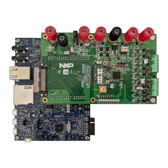
- Page 38 UM11565 NXP Semiconductors NAFExx388 evaluation board Figures Fig. 1. NAFExx388 evaluation board paired with Fig. 23. Voltage values ..........28 OM13098 (LPC54628) evaluation board ...8 Fig. 24. Save AFE configuration ........28 Fig. 2. Test setup showing connectivity between Fig. 25.
-
Page 39: Table Of Contents
Please be aware that important notices concerning this document and the product(s) described herein, have been included in section 'Legal information'. © 2023 NXP B.V. All rights reserved. For more information, please visit: http://www.nxp.com Date of release: 29 March 2023 Document identifier: UM11565...
Need help?
Do you have a question about the UM11565 and is the answer not in the manual?
Questions and answers