Table of Contents
Advertisement
Quick Links
Advertisement
Table of Contents

Related Manuals for Alpha Data ADM-XRC-7Z1


Summary of Contents for Alpha Data ADM-XRC-7Z1
- Page 1 ADM-XRC-7Z1 User Manual Document Revision: 2.6 14th February 2022...
- Page 2 ADM-XRC-7Z1 User Manual V2.6 - 14th February 2022 © 2022 Copyright Alpha Data Parallel Systems Ltd. All rights reserved. This publication is protected by Copyright Law, with all rights reserved. No part of this publication may be reproduced, in any shape or form, without prior written consent from Alpha Data Parallel Systems Ltd.
-
Page 3: Table Of Contents
ADM-XRC-7Z1 User Manual V2.6 - 14th February 2022 Table Of Contents Overview ............................1 Introduction ............................ 1 Key Features ..........................1 Order Code ............................ 2 References & Specifications ......................2 PCB Information ..........................3 Physical Specifications ........................3 Motherboard / Carrier Requirements ..................... 3 Power Requirements ........................ - Page 4 ADM-XRC-7Z1 User Manual V2.6 - 14th February 2022 4.8.2.3 PS DDR3 Memory ....................... 13 4.8.3 Ethernet Interfaces ........................13 4.8.4 Serial COM Ports ........................15 4.8.5 USB Interfaces ......................... 15 Zynq PL Block ..........................15 4.9.1 PL DDR3 Memory ........................15 4.9.2...
- Page 5 Table 30 XRM Connector CN2 ........................28 Table 31 XMC Connector P5 .......................... 29 List of Figures Figure 1 ADM-XRC-7Z1 Block Diagram ......................5 Figure 2 LED Locations ........................... 7 Figure 3 Ethernet Interfaces .......................... 13 Figure 4 Serial COM Ports ..........................15 Figure 5 USB Interfaces ..........................
- Page 6 ADM-XRC-7Z1 User Manual V2.6 - 14th February 2022 Page Intentionally left blank...
-
Page 7: Overview
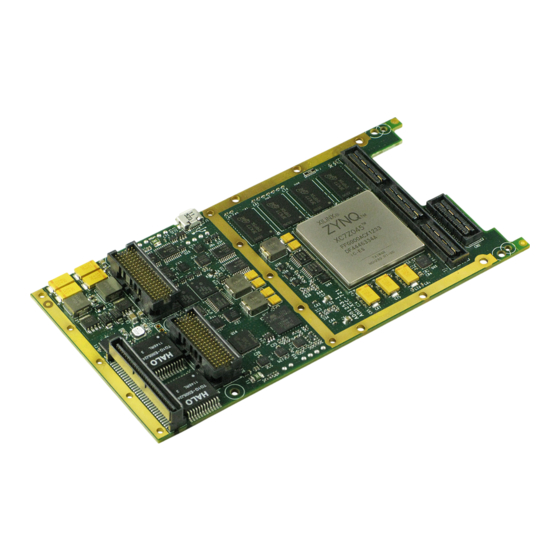
ADM-XRC-7Z1 User Manual V2.6 - 14th February 2022 1 Overview 1.1 Introduction The ADM-XRC-7Z1 ("7Z1") is a high-performance Processor XMC for applications using Zynq-7000 SoCs from Xilinx. 1.2 Key Features Key Features • Single-width XMC, compliant to VITA Standard 42.0, 42.3 and 42.10d12 •... -
Page 8: Order Code
/AC1 = air cooled industrial /CC1 = conduction cooled industrial Table 1 : Build Options Not all combinations are available. Please check with Alpha Data sales for details. 1.4 References & Specifications ANSI/VITA 42.0 XMC Standard, December 2008, VITA, ISBN 1-885731-49-3 ANSI/VITA 42.3... -
Page 9: Pcb Information
VITA standard. It is important to check carrier card compatibility prior to installation. If in doubt, please contact Alpha Data for assistance. IMPORTANT Connector P4 has +5V (power) -/+6V (serial port) levels. It must not be connected to the Alpha Data ADM-EMC-II or ADM-XMC-II carrier cards. Please contact Alpha Data for carrier card compatibility. 2.3 Power Requirements The power dissipation of the board is highly dependent on the Target FPGA application. -
Page 10: Installation
ADM-XRC-7Z1 User Manual V2.6 - 14th February 2022 3 Installation 3.1 Software Installation Please refer to the Software Development Kit (SDK) installation CD. The SDK contains drivers, examples for host control and FPGA design and comprehensive help on application interfacing. -
Page 11: Functional Description
Programmable Logic (PL) DDR3 SDRAM GPIO PCIE/HSSIO (7:0) (256MB) (x146) Clocks DDR3 SDRAM GTX Transceivers P6 RefClk XRM I/F (256MB) (7:0) (8:11) (15:12) (Front IO) GPIO (x38) HSSIO (15:8) HSSIO (x8) Figure 1 : ADM-XRC-7Z1 Block Diagram Functional Description Page 5 ad-ug-1253_v2_6.pdf... -
Page 12: Switch Definitions
ADM-XRC-7Z1 User Manual V2.6 - 14th February 2022 4.1.1 Switch Definitions There are two sets of 8-way DIP switches for configuring the board. Switch 1 Ref. Function OFF State ON State SW1-1 Reserved Flash Boot SW1-2 Allow PS to boot PL from flash... -
Page 13: Led Definitions
ADM-XRC-7Z1 User Manual V2.6 - 14th February 2022 4.1.2 LED Definitions There are seven LEDs to provide a visual indication of the board status. Their locations are shown in Figure 2 MVMRO DONE PWRFLT ETH1 ETH0 SWRST SYS 0 SYS 1 Figure 2 : LED Locations Comp. -
Page 14: Primary Xmc Connector P5
ADM-XRC-7Z1 User Manual V2.6 - 14th February 2022 A further two sets of three LEDs provide an indication of the status of the two Ethernet interfaces Comp. Ref. Function ON State Off State Ethernet 0 D23 (Green) Table 16 LED0... -
Page 15: Mpresent
The Transmit (Tx) side of all eight lanes are AC coupled by 100nF capacitors, placed at the output from the PL. The Receive (Rx) side of all eight lanes are directly connected from the connector to the PL. Alternative coupling options are available as a special ordering option. Please contact Alpha Data for details. 4.3 Secondary XMC Connector P6... -
Page 16: Jtag Interfaces
ADM-XRC-7Z1 User Manual V2.6 - 14th February 2022 4.5 JTAG Interfaces 4.5.1 On-board Interface By default, the 7Z1 is configured to have a single (cascaded) JTAG scan chain connected to header J4. This allows the connection of the Xilinx JTAG cable for debug using the Xilinx ChipScope tools. -
Page 17: P6 Reference Clock (P6Refclk)
ADM-XRC-7Z1 User Manual V2.6 - 14th February 2022 Signal Target FPGA Input IO Standard "P" pin "N" pin PCIEREFCLK MGTREFCLK0_112 HSCL Table 8 : PCIEREFCLK Connections 4.6.2 P6 Reference Clock (P6REFCLK) A reference clock can be provided by the carrier card through the Secondary XMC connector, P6, at pins A19 and B19. -
Page 18: Refclk200M
ADM-XRC-7Z1 User Manual V2.6 - 14th February 2022 4.6.5 REFCLK200M The fixed 200MHz reference clock, REFCLK200M, is a differential clock signal using LVDS. Three phase-matched copies are distributed to Global Clock inputs on the Zynq PL. This clock can be used to generate application-specific clock frequencies using the PLLs within the Zynq PL. It is also suitable as the reference clock for the IO delay control block (IDELAYCTRL) and memory interfaces. -
Page 19: Zynq Ps Block
ADM-XRC-7Z1 User Manual V2.6 - 14th February 2022 4.8 Zynq PS Block 4.8.1 Boot Modes BootSel1 BootSel0 Boot Mode (SW2-2) (SW2-1) JTAG Quad SPI SD Flash Reserved Table 15 : Boot Mode Selection 4.8.2 PS Memory Interfaces 4.8.2.1 Quad SPI Flash Memory 512Mb of QSPI flash memory (Micron N25Q256A11E1240E/MT41K128M16JT) is attached to the PS, and is used to store Zynq boot images, FPGA bitstreams and data. -
Page 20: Table 16 Ethernet Status Leds
ADM-XRC-7Z1 User Manual V2.6 - 14th February 2022 Colour Function Green Green Amber Table 16 : Ethernet Status LEDs Page 14 Functional Description ad-ug-1253_v2_6.pdf... -
Page 21: Serial Com Ports
There are two serial COM ports connected to PMC connector P4, as shown in Figure Serial COM Ports. COM2 uses RS-232 by default but may be configured for RS-485 operation. Please contact Alpha Data for further details of the RS-485 mode. COM0... -
Page 22: Xrm Connector, Cn1
ADM-XRC-7Z1 User Manual V2.6 - 14th February 2022 4.9.2.1 XRM Connector, CN1 Connector CN1 is for general purpose signals, power and module control. The connector is a 180-way Samtec connector with 3 fields. The part fitted to the ADM-XRC-KU1 is Samtec QSH-090-01-F-D-A-K. -
Page 23: Gtx Links
ADM-XRC-7Z1 User Manual V2.6 - 14th February 2022 details on duplicating this VPD data. Alternatively, FORCE2V5_L can be driven low to select 1.8V for the front I/O voltage. Note that FORCE2V5_L is a signal name from a historical design, and the operating voltage will not be 2.5V but rather 1.8V if this mode is used. -
Page 24: Rear Gpio Interface
ADM-XRC-7Z1 User Manual V2.6 - 14th February 2022 Signal FPGA + Pin FPGA - Pin Rear Connector + Pin Rear Connector - Pin P6_TX_6 P6.A7 P6.B7 P6_TX_7 P6.D7 P6.E7 P6_RX_0 P6.A11 P6.B11 P6_RX_1 P6.D11 P6.E11 P6_RX_2 P6.A13 P6.B13 P6_RX_3 P6.D13 P6.E13... -
Page 25: System Monitoring
ADM-XRC-7Z1 User Manual V2.6 - 14th February 2022 4.10 System Monitoring The 7Z1 has the ability to monitor temperature and voltage to maintain a check on the operation of the board. The monitoring is implemented using an Atmel AVR microcontroller (uC). -
Page 26: System Monitor Status Leds
ADM-XRC-7Z1 User Manual V2.6 - 14th February 2022 Target FPGA Board (uC and PCB) Lower Upper Lower Upper Warning Warning Warning Warning Commercial -5°C +5°C +80°C +90°C -5°C +5°C +65°C +75°C Extended -5°C +5°C +95°C +105°C -5°C +5°C +80°C +90°C Industrial -45°C... -
Page 27: Appendix A Rear Connector Pinouts
ADM-XRC-7Z1 User Manual V2.6 - 14th February 2022 Appendix A: Rear Connector Pinouts Appendix A.1: Primary XMC Connector, P5 PET0p0 PET0n0 3.3V PET0p1 PET0n1 VPWR XMC_TRST# MRSTI# PET0p2 PET0n2 3.3V PET0p3 PET0n3 VPWR XMC_TCK MRSTO# PET0p4 PET0n4 3.3V PET0p5 PET0n5... -
Page 28: Secondary Xmc Connector, P6
ADM-XRC-7Z1 User Manual V2.6 - 14th February 2022 Appendix A.2: Secondary XMC Connector, P6 P6_TXp0 P6_TXn0 GPIO_18P P6_TXp1 P6_TXn1 GPIO_18N GPIO_16N GPIO_17N P6_TXp2 P6_TXn2 GPIO_16P P6_TXp3 P6_TXn3 GPIO_17P GPIO_14N GPIO_15N P6_TXp4 P6_TXn4 GPIO_14P P6_TXp5 P6_TXn5 GPIO_15P GPIO_12N GPIO_13N P6_TXp6 P6_TXn6... -
Page 29: Pmc Connector P4
ADM-XRC-7Z1 User Manual V2.6 - 14th February 2022 Appendix A.3: PMC Connector P4 Signal Pin J14 Pin J14 Signal ETH0_DA+ ETH0_DC+ ETH0_DA- ETH0_DC- ETH0_DB+ ETH0_DD+ ETH0_DB- ETH0_DD- ETH1_DA+ ETH1_DC+ ETH1_DA- ETH1_DC- ETH1_DB+ ETH1_DD+ ETH1_DB- ETH1_DD- USB1_D- USB2_D- USB1_D+ USB2_D+ USB1_VCC... -
Page 30: Appendix B Front (Xrm) Connector Pinouts
ADM-XRC-7Z1 User Manual V2.6 - 14th February 2022 Appendix B: Front (XRM) Connector Pinouts The XRM interface consists of two connectors: CN1 and CN2. CN1 is a 180-way Samtec QSH in 3 fields. It is for general-purpose signals, power and module control. CN2 is a 28-way Samtec QSE-DP for high-speed serial (MGT) links. -
Page 31: Xrm Connector Cn1, Field 1
ADM-XRC-7Z1 User Manual V2.6 - 14th February 2022 Appendix B.1: XRM Connector CN1, Field 1 Signal FPGA Samtec Samtec FPGA Signal DA_N0 DA_N1 DA_P0 DA_P1 DA_N2 DA_P3 DA_P2 DA_N3 DA_N4 DA_N5 DA_P4 DA_P5 DA_N6 DA_N7 DA_P6 DA_P7 DA_P8 DA_P9 DA_N8... -
Page 32: Xrm Connector Cn1, Field 2
ADM-XRC-7Z1 User Manual V2.6 - 14th February 2022 Appendix B.2: XRM Connector CN1, Field 2 Signal FPGA Samtec Samtec FPGA Signal DB_N2 DB_N3 DB_P2 DB_P3 DB_N4 DB_N5 DB_P4 DB_P5 DB_N6 AA28 AE26 DB_N7 DB_P6 AA27 AD25 DB_P7 DB_N8 AC27 AD30... -
Page 33: Xrm Connector Cn1, Field 3
ADM-XRC-7Z1 User Manual V2.6 - 14th February 2022 Appendix B.3: XRM Connector CN1, Field 3 Signal FPGA Samtec Samtec FPGA Signal DC_P2 AJ30 AC29 DC_P3 DC_N2 AK30 AD29 DC_N3 DC_N4 AF27 AF30 DC_P5 DC_P4 AE27 AG30 DC_N5 DC_P6 AK22 AF29... -
Page 34: Xrm Connector Cn2
ADM-XRC-7Z1 User Manual V2.6 - 14th February 2022 Appendix B.4: XRM Connector CN2 Signal FPGA Samtec Samtec FPGA Signal MGT_C2M_P0 MGT_M2C_P0 MGT_C2M_N0 MGT_M2C_N0 MGT_C2M_P1 MGT_M2C_P1 MGT_C2M_N1 MGT_M2C_N1 MGT_C2M_P4 AK10 AH10 MGT_M2C_P4 MGT_C2M_N4 MGT_M2C_N4 MGT_C2M_P5 MGT_M2C_P5 MGT_C2M_N5 MGT_M2C_N5 MGT_C2M_P2 MGT_M2C_P2 MGT_C2M_N2... -
Page 35: Appendix C Xmc Breakout Fpga Pinout
Appendix C: XMC Breakout FPGA Pinout The pinout below applies when using the ADM-XRC-7Z1 with the ADC-XMC-BREAKOUT. This table only shows pins that are connected to the FPGA, for the pinout of other interfaces (e.g. Ethernet, USB ...etc, see the ADM-XRC-7Z1 reference design). - Page 36 ADM-XRC-7Z1 User Manual V2.6 - 14th February 2022 Revision History Date Revision Nature of Change Initial Release 03/07/13 Minor Updates 04/10/13 Updated for rev2 board, Clarified key features, Figure 1: corrected QSPI size, Table 5: corrected SW2-5 and SW2-6 descriptions to match rev2 PCB, 4.2.1.2: MBIST is not used, 4.2.1.4: Added description of External Reset...
Need help?
Do you have a question about the ADM-XRC-7Z1 and is the answer not in the manual?
Questions and answers