Table of Contents
Advertisement
Quick Links
Advertisement
Table of Contents

Related Manuals for Alpha Data ADM-XRC-7V1


Summary of Contents for Alpha Data ADM-XRC-7V1
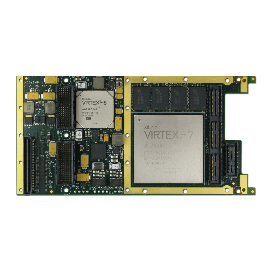
- Page 1 ADM-XRC-7V1 User Manual Document Revision: 1.9 23rd Aug 2016...
- Page 2 ADM-XRC-7V1 User Manual V1.9 - 23rd Aug 2016 © 2016 Copyright Alpha Data Parallel Systems Ltd. All rights reserved. This publication is protected by Copyright Law, with all rights reserved. No part of this publication may be reproduced, in any shape or form, without prior written consent from Alpha Data Parallel Systems Ltd.
-
Page 3: Table Of Contents
ADM-XRC-7V1 User Manual V1.9 - 23rd Aug 2016 Table Of Contents Introduction ............................1 Key Features ..........................1 References & Specifications ......................1 Installation ............................2 Software Installation ........................2 Hardware Installation ........................2 2.2.1 Handling Instructions ......................... 2 2.2.2 Motherboard / Carrier Requirements .................. - Page 4 Table 24 XRM Connector CN1, Field 3 ......................33 Table 25 XRM Connector CN2 ........................34 List of Figures Figure 1 ADM-XRC-7V1 Block Diagram ......................4 Figure 2 LED Locations ........................... 6 Figure 3 JTAG Header J1 ..........................8 Figure 4 JTAG Boundary Scan Chain ......................
-
Page 5: Introduction
(target) FPGA. With the release of 7series FPGA boards, Alpha Data has introduced a new build option to allow the mezzanine card to be assembled without the bridge to reduce power and cost. -
Page 6: Installation
- Store in ESD safe bag. 2.2.2 Motherboard / Carrier Requirements The ADM-XRC-7V1 is a single width XMC.3 mezzanine with optional P6 and P4 connectors. The motherboard/ carrier must comply with the XMC.3 (VITA 42.3) specification for the Primary XMC connector, J5. - Page 7 ADM-XRC-7V1 User Manual V1.9 - 23rd Aug 2016 Solutions. The board features system monitoring that measures the board and FPGA temperature. It also includes a self-protection mechanism that will clear the target FPGA configuration if an over-temperature condition is detected.
-
Page 8: Functional Description
28-Way (FFG/FLG/FHG 1761) DDR3 Bank3 (HR) Unused FPGA Banks GPIO Level HR banks in X330T and 585T Converter 64 GPIO 12 (HR) Quick Switch Not in X330T and X485T Figure 1 : ADM-XRC-7V1 Block Diagram Page 4 Functional Description ad-ug-1248_v1_9.pdf... -
Page 9: Switch Definitions
ADM-XRC-7V1 User Manual V1.9 - 23rd Aug 2016 3.1.1 Switch Definitions There is a set of eight DIP switches placed on the rear of the board. Their functions are described in Switch Definitions. Note: All switches are OFF by default. Factory Configuration switch must be in the OFF position for normal operation. -
Page 10: Led Definitions
ADM-XRC-7V1 User Manual V1.9 - 23rd Aug 2016 3.1.2 LED Definitions The position and description of the board status LEDs are shown in Locations: Status 1 Status 2 Target Done D10 Bridge Done D11 Bridge-Bypass D12 Bridge-Less Figure 2 : LED Locations Comp. -
Page 11: Xmc Platform Interface
ADM-XRC-7V1 User Manual V1.9 - 23rd Aug 2016 3.2 XMC Platform Interface 3.2.1 IPMI I2C A 4 Kbit I2C EEPROM (type M24C04) is connected to the XMC IPMI. This memory contains board information (type, voltage requirements etc.) as defined in the XMC based specification. -
Page 12: Jtag Interface
ADM-XRC-7V1 User Manual V1.9 - 23rd Aug 2016 3.3 JTAG Interface 3.3.1 On-board Interface A JTAG boundary scan chain is connected to header J1. This allows the connection of the Xilinx JTAG cable for FPGA debug using the Xilinx ChipScope tools. -
Page 13: Clocks
4 user-programmable clocks. These clocks can be combined with the FPGA's internal PLLs to suit a wide variety of communication protocols. A complete overview of the clock routing on the ADM-XRC-7V1 is given in Clocks. A description of each clock follows. -
Page 14: 200Mhz Reference Clock (Refclk200M)
MGT signal inputs. Most needed reference clocks can be generated through the User Programmable clocking options. If it is a requirement that this differential pair be utilized as a clock signal to an MGT bank, a resistor fit option is available. Please contact Alpha Data for detials. Page 10 Functional Description ad-ug-1248_v1_9.pdf... -
Page 15: Programmable Clocks (Lclk, Progclk 0-3)
There are two programable clock sources that are forwarded throughout the FPGA. These clocks are programmable through the Alpha Data ADM-XRC Gen 3 SDK. LCLK is generated in the Bridge FPGA by the the Alpha Data ADB3 driver and offers a less accurate frequency resolution, but with a wider programmable frequency range. -
Page 16: Table 9 Xrm_Lvds_Clk Connections
ADM-XRC-7V1 User Manual V1.9 - 23rd Aug 2016 Signal Frequency Target FPGA Input IO Standard "P" pin "N" pin XRM_PECL_CLK Variable IO_L13_T2_MRCC_15 LVDS AV40 AW40 Table 9 : XRM_LVDS_CLK Connections Page 12 Functional Description ad-ug-1248_v1_9.pdf... -
Page 17: Flash Memory
FLPAGE and FLDATA registers in the Bridge FPGA. The region of memory between addresses 0x11000000 and 0x11FFFFF is allocated for custom data to be stored by the ADM-XRC-7V1 user. Utilities for erasing, programming and verification of the flash memory are provided in the ADMXRC SDK. -
Page 18: Configuration
ADM-XRC-7V1 User Manual V1.9 - 23rd Aug 2016 3.6 Configuration 3.6.1 Power-Up Sequence If valid data is stored in the flash memory, the bridge will automatically configure the Target FPGA at power-up. This sequence can be inhibited by turning the Flash Boot Inhibit (FBI) switch, SW1-4 to ON. (See Switch Definitions). -
Page 19: Health Monitoring
V1.9 - 23rd Aug 2016 3.7 Health Monitoring The ADM-XRC-7V1 has the ability to monitor temperature and voltage to maintain a check on the operation of the board. The monitoring is implemented using the ATMEGA64 microcontroller. Control algorithms within the microcontroller automatically check line voltages and on board temperaturs and shares the information with blockram in the Bridge FPGA. -
Page 20: Automatic Temperature Monitoring
ADM-XRC-7V1 User Manual V1.9 - 23rd Aug 2016 3.7.1 Automatic Temperature Monitoring The onboard system monitor microcontroller contains pre-programmed temperature limits. The temperature limits are shown in Table Temperature Limits: Target FPGA Bridge FPGA Board Commercial 0 degC +85 degC... -
Page 21: Local Bus
ADM-XRC-7V1 User Manual V1.9 - 23rd Aug 2016 3.8 Local Bus A Multiplexed Packet Transport Link (MPTL) connects the Bridge and Target FPGAs. It is capable of transferring data at up to 2GB/s simultaneously in each direction. The MPTL replaces the parallel local bus used in previous generations of the ADM-XRC series. Details of the link and example designs are given in the Software Development Kit (SDK). -
Page 22: Figure 7 Mgt Links
ADM-XRC-7V1 User Manual V1.9 - 23rd Aug 2016 7 Series MGT/ Banks MGT119 PCIe Bridge RearMGT(3:0) MGT118 MGT117 Bridge Bypass MGT116 RearMGT(7:4) MGT115 RearMGT(8:11) MGT114 RearMGT(12:15) RearMGT(16:17) MGT113 MGT112 MGT111 XRM(3:0) XRM(7:4) XRM Interface Figure 7 : MGT Links Page 18 Functional Description ad-ug-1248_v1_9.pdf... -
Page 23: Memory Interfaces
V1.9 - 23rd Aug 2016 3.10 Memory Interfaces The ADM-XRC-7V1 has four independent banks of DDR3 SDRAM. Each bank consists of two 16 bit wide memory devices in parallel to provide a 32 bit datapath capable of running up to 800MHz (DDR-1600). 2Gb devices (Micron MT41J64M16-187E) are fitted as standard to provide 512MB per bank. -
Page 24: Xrm Interface And Front-Panel I/O
The XRM interface provides a high-performance and flexible front-panel interface through a range of interchangeable XRM modules. Further details of the XRM modules can be found on the Alpha Data website. The XRM interface consists of two samtec connectors, CN1 and CN2. -
Page 25: Xrm I/F - High-Speed Serial Links
VPD data. Alternatively, if using an ADM-XRC-7V1 rev 4 or newer, FORCE2V5_L can be driven low to select 1.8V for the front I/O voltage. Note that FORCE2V5_L is a signal name from a historical design, and the operating voltage will not be 2.5V but rather 1.8V if this mode is used. - Page 26 ADM-XRC-7V1 User Manual V1.9 - 23rd Aug 2016 Page Intentionally left blank Page 22 Functional Description ad-ug-1248_v1_9.pdf...
-
Page 27: Appendix A Rear Connector Pinouts
ADM-XRC-7V1 User Manual V1.9 - 23rd Aug 2016 Appendix A: Rear Connector Pinouts Appendix A.1: Primary XMC Connector, P5 PET_PO PET_NO PET_P1 PET_N1 VPWR TRST_L MRSTI_L PET_P2 PET_N2 PET_P3 PET_N3 VPWR MRSTO_L PET_P4 PET_N4 PET_P5 PET_N5 VPWR 12V0 PET_P6 PET_N6... -
Page 28: Secondary Xmc Connector, P6
ADM-XRC-7V1 User Manual V1.9 - 23rd Aug 2016 Appendix A.2: Secondary XMC Connector, P6 PN6_TX_P0 PN6_TX_N0 GP37 PN6_TX_P1 PN6_TX_N1 GP38 GP35 GP36 PN6_TX_P2 PN6_TX_N2 GP33 PN6_TX_P3 PN6_TX_N3 GP34 GP31 GP32 PN6_TX_P4 PN6_TX_N4 GP29 PN6_TX_P5 PN6_TX_N5 GP30 GP27 GP28 PN6_TX_P6 PN6_TX_N6... -
Page 29: Pn6 Gpio Pin Map
ADM-XRC-7V1 User Manual V1.9 - 23rd Aug 2016 Appendix A.2.1: Pn6 GPIO Pin Map Signal FPGA Pin FPGA Bank BA32 BA30 BA31 BB31 AW31 AY32 AV30 AY30 AV35 GP10 AR35 GP11 AW33 GP12 AV33 GP13 AV34 GP14 AY33 GP15 AT35... - Page 30 ADM-XRC-7V1 User Manual V1.9 - 23rd Aug 2016 Signal FPGA Pin FPGA Bank GP35 AN30 GP36 AL32 GP37 AL31 GP38 AN31 Table 19 : Pn6 GPIO Pin Map GCC: Global clock capable MRCC: Multi-region clock capable SRCC: Single-region clock capable...
-
Page 31: Pmc Connector P4
ADM-XRC-7V1 User Manual V1.9 - 23rd Aug 2016 Appendix A.3: PMC Connector P4 Clock Clock Signal FPGA Pin P4 Pin P4 Pin FPGA Pin Signal Capability Capability PN4_P1 AK20 AJ21 PN4_P2 PN4_N1 AL20 AJ20 PN4_N2 PN4_P3 AJ23 AJ22 PN4_P4 PN4_N3... -
Page 32: Rear Mgt Connections To The Target Fpga
ADM-XRC-7V1 User Manual V1.9 - 23rd Aug 2016 Appendix A.4: Rear MGT Connections to the Target FPGA In normal mode, the target FPGA RearMGT lanes (3:0) are connected to the Bridge FPGA. In Bridge Bypass Mode, they are connected to P5 lanes (3:0). - Page 33 ADM-XRC-7V1 User Manual V1.9 - 23rd Aug 2016 Signal FPGA + Pin FPGA - Pin Rear Connector + Pin Rear Connector - Pin RearMGT_RX_10 P6.A13 P6.B13 RearMGT_RX_11 P6.D13 P6.E13 RearMGT_RX_12 P6.A15 P6.B15 RearMGT_RX_13 P6.D15 P6.E15 RearMGT_RX_14 P6.A17 P6.B17 RearMGT_RX_15 P6.D17 P6.E17...
-
Page 34: Appendix B Front (Xrm) Connector Pinouts
ADM-XRC-7V1 User Manual V1.9 - 23rd Aug 2016 Appendix B: Front (XRM) Connector Pinouts The XRM interface consists of two connectors: CN1 and CN2. CN1 is a 180-way Samtec QSH in 3 fields. It is for general-purpose signals, power and module control. CN2 is a 28-way Samtec QSE-DP for high-speed serial (MGT) links. -
Page 35: Xrm Connector Cn1, Field 1
ADM-XRC-7V1 User Manual V1.9 - 23rd Aug 2016 Appendix B.1: XRM Connector CN1, Field 1 Signal FPGA Samtec Samtec FPGA Signal DA_N0 AE35 AD31 DA_N1 DA_P0 AE34 AC31 DA_P1 DA_N2 AB31 DA_P3 DA_P2 AB32 DA_N3 DA_N4 AE33 DA_N5 DA_P4 AE32... -
Page 36: Xrm Connector Cn1, Field 2
ADM-XRC-7V1 User Manual V1.9 - 23rd Aug 2016 Appendix B.2: XRM Connector CN1, Field 2 Signal FPGA Samtec Samtec FPGA Signal DB_N2 AD37 AV41 DB_N3 DB_P2 AD36 AU41 DB_P3 DB_N4 AA37 AH36 DB_N5 DB_P4 AG36 DB_P5 DB_N6 AG34 AW42 DB_N7... -
Page 37: Xrm Connector Cn1, Field 3
ADM-XRC-7V1 User Manual V1.9 - 23rd Aug 2016 Appendix B.3: XRM Connector CN1, Field 3 Signal FPGA Samtec Samtec FPGA Signal DC_P2 AP41 AR38 DC_P3 DC_N2 AP42 AR39 DC_N3 DC_N4 BB39 AW37 DC_P5 DC_P4 BB38 AY37 DC_N5 DC_P6 AR42 AY39... -
Page 38: Xrm Connector Cn2
ADM-XRC-7V1 User Manual V1.9 - 23rd Aug 2016 Appendix B.4: XRM Connector CN2 Signal FPGA Samtec Samtec FPGA Signal MGT_C2M_P0 MGT_M2C_P0 MGT_C2M_N0 MGT_M2C_N0 MGT_C2M_P1 MGT_M2C_P1 MGT_C2M_N1 MGT_M2C_N1 MGT_C2M_P4 MGT_M2C_P4 MGT_C2M_N4 MGT_M2C_N4 MGT_C2M_P5 MGT_M2C_P5 MGT_C2M_N5 MGT_M2C_N5 MGT_C2M_P2 MGT_M2C_P2 MGT_C2M_N2 MGT_M2C_N2 MGT_C2M_P3... - Page 39 ADM-XRC-7V1 User Manual V1.9 - 23rd Aug 2016 Revision History Date Revision Changed By Nature of Change Initial Draft 21 Mar 2012 K. Roth Initial Release 10 Aug 2012 K. Roth Added note to PN4 Appendix regarding LVDS, fixed P6 17 Aug 2012 K.
Need help?
Do you have a question about the ADM-XRC-7V1 and is the answer not in the manual?
Questions and answers