Table of Contents
Advertisement
Quick Links
Advertisement
Table of Contents

Related Manuals for Alpha Data ADM-PCIE-9V5


Summary of Contents for Alpha Data ADM-PCIE-9V5
- Page 1 ADM-PCIE-9V5 User Manual Document Revision: 1.0 29th August 2019...
- Page 2 ADM-PCIE-9V5 User Manual © 2019 Copyright Alpha Data Parallel Systems Ltd. All rights reserved. This publication is protected by Copyright Law, with all rights reserved. No part of this publication may be reproduced, in any shape or form, without prior written consent from Alpha Data Parallel Systems Ltd.
-
Page 3: Table Of Contents
ADM-PCIE-9V5 User Manual Table Of Contents Introduction ............................1 Key Features ..........................1 Order Code ............................ 1 Board Information ..........................2 Physical Specifications ........................2 Chassis Requirements ........................3 2.2.1 PCI Express ..........................3 2.2.2 Mechanical Requirements ......................3 2.2.3 Power Requirements ......................... - Page 4 ADM-PCIE-9V5 Top View ........................2 Figure 3 Thermal Performance ........................4 Figure 4 ADM-PCIE-9V5 Fan .......................... 5 Figure 5 ADM-PCIE-9V5 2-slot enhanced heat sink ..................5 Figure 6 ADM-PCIE-9V5 Block Diagram ......................6 Figure 7 Switches ............................7 Figure 8 Front Panel LEDs ..........................
-
Page 5: Introduction
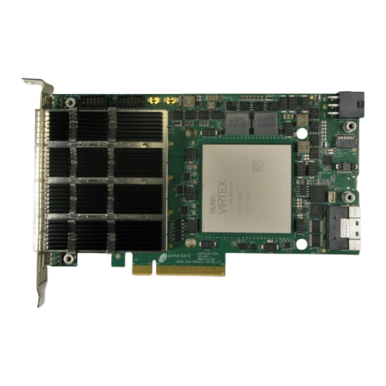
ADM-PCIE-9V5 User Manual 1 Introduction The ADM-PCIE-9V5 is a high-performance reconfigurable computing card intended for Data Center applications, featuring a screened Xilinx Virtex UltraScale+ Plus FPGA with low latency transceivers and four QSFP-DD cages. Figure 1 : ADM-PCIE-9V5 Product Photo 1.1 Key Features... -
Page 6: Board Information
ADM-PCIE-9V5 User Manual 2 Board Information 2.1 Physical Specifications The ADM-PCIE-9V5 complies with PCI Express CEM revision 3.0. Description Measure Total Dy 120.9 mm PCB Dy 100.15 mm Total Dx 181.5 mm PCB Dx 167.65 mm Total Dz 19.7 mm... -
Page 7: Chassis Requirements
2.2 Chassis Requirements 2.2.1 PCI Express The ADM-PCIE-9V5 is capable of PCIe Gen 3 with 8 lanes, using the Xilinx Integrated Block for PCI Express. 2.2.2 Mechanical Requirements An 8 or 16 lane physical PCIe slot is required for mechanical compatibility. -
Page 8: Thermal Performance
If the FPGA core temperature exceeds 105 degrees Celsius, the FPGA design will be cleared to prevent the card from over-heating. The ADM-PCIE-9V5 comes with a heat sink to help avoid thermal overstress of FPGA, since it is typically the hottest point on the card. The FPGA die temperature must remain under 100 degrees Celsius. To calculate the FPGA die temperature, take your application power, multiply by Theta JA from the table below, and add to your system internal ambient temperature. -
Page 9: Active Vs Passive Thermal Management
2.3.1 Active VS Passive Thermal Management The ADM-PCIE-9V5 ships with a small optional blower for active cooling in systems with poor airflow. If the ADM-PCIE-9V5 will be installed in a server with controlled airflow, the card may be ordered without the additional fan hardware. -
Page 10: Functional Description
3 Functional Description 3.1 Overview The ADM-PCIE-9V5 is a versatile reconfigurable computing platform with a Virtex UltraScale+ VU5P/VU9P FPGA, a Gen3x8 PCIe interface, four QSFP-DD cages, an OpenCAPI compatible Ultraport SlimSAS connector also capable of 28G/channel, an isolated input for a timing synchronization pulse, a 12 pin header for general purpose use (clocking, control pins, debug, etc.), front panel LEDs, and a robust system monitor. -
Page 11: Switches
ADM-PCIE-9V5 User Manual 3.1.1 Switches The ADM-PCIE-9V5 has an octal DIP switch SW1, located on the rear side of the board. The function of each switch in SW1 is detailed below: Figure 7 : Switches Factory Switch Function OFF State... -
Page 12: Leds
ADM-PCIE-9V5 User Manual 3.1.2 LEDs There are 9 LEDs on the ADM-PCIE-9V5, 6 of which are general purpose and whose meaning can be defined by the user. The other 3 have fixed functions described below: User LEDs Status LEDs LED_G2... -
Page 13: Clocking
FPGA fabric. Any programmable clock, from the SI5338 Clock Synthesizer, is re-configurable from the front panel USB Interface by using Alpha Data’s avr2util utility. This allows the user to configure almost any arbitrary clock frequency during application run time. The maximum clock frequency is 312.5MHz. Customers who purchase RD-9V5 also have the option of embedding IP into their FPGA design that permits programmable clock re-configuration via PCIe or from within the FPGA. -
Page 14: Figure 10 Vu5P Fpga Clock Location
ADM-PCIE-9V5 User Manual GTY Quad 233 GTY Quad 133 CMAC HP I/O Bank 53 HP I/O Bank 73 ILKN X1Y36 – X1Y39 QSFP-DD 0 lanes 4 - 7 X0Y36 - X0Y39 X0Y5 X1Y5 G [RN] SI5328_0_OUT_1 GTY Quad 132 GTY Quad 232... -
Page 15: Figure 11 Vu9P Fpga Clock Location
ADM-PCIE-9V5 User Manual GTY Quad 233 GTY Quad 133 CMAC HP I/O Bank 73 ILKN X1Y56 – X1Y59 HP I/O Bank 53 QSFP-DD 0 lanes 4 - 7 X0Y56 - X0Y59 X0Y8 X1Y8 G [RN] SI5328_0_OUT_1 GTY Quad 232 GTY Quad 132... -
Page 16: Si5328
ADM-PCIE-9V5 User Manual 3.2.1 Si5328 If jitter attenuation is required please see the reference documentation for the Si5328. https://www.silabs.com/Support%20Documents/TechnicalDocs/Si5328.pdf The circuit connections mirror the Xilinx VCU110 and VCU108 Development Kits. Please refer to the Xilinx documentation for information. The CLKIN2 input of the SI5328, provided by the SI5338, is only available in rev2 PCBs and onward (Serial number greater than 109). -
Page 17: Pci Express
3.3 PCI Express The ADM-PCIE-9V5 is capable of PCIe Gen 3 with 8 lanes. The FPGA drives these lanes directly using the Integrated PCI Express block from Xilinx. Negotiation of PCIe link speed and number of lanes used is generally automatic and does not require user intervention. -
Page 18: Qsfp-Dd
Figure 12 : QSFP-DD Location It is possible for Alpha Data to pre-fit the ADM-PCIE-9V5 with QSFP-DD and QSFP28 components. Please contact sales@alpha-data.com for full details and options. Alpha Data has tested the ADM-PCIE-9V5 with an array of passive cables from multiple manufacturers. Please contact sales@alpha-data.com for more details on appropriate and available cables. -
Page 19: Opencapi Ultraport Slimsas
200G (8 channels at 25G). Please contact support@alpha-data.com or your IBM representative for more details on OpenCAPI and its benefits. The SlimSAS connector can also be used to connect multiple ADM-PCIE-9V5 cards within a chassis. Figure 13 : OpenCAPI Location... -
Page 20: System Monitor
3.6 System Monitor The ADM-PCIE-9V5 has the ability to monitor its own temperature and the voltages and currents of certain power supply rails, in order to provide an indication of board health. The monitoring is implemented using an Atmel AVR microcontroller. -
Page 21: System Monitor Status Leds
ADM-PCIE-9V5 User Manual 3.6.1 System Monitor Status LEDs LEDs D5 (Red) and D7 (Green) indicate the card health status. LEDs Status Green Running and no alarms Green + Red Standby (Powered off) Flashing Green + Flashing Red Attention - critical alarm active... -
Page 22: Usb Interface
The ADM-PCIE-9V5 utilizes the Digilent USB-JTAG converter box which is supported by the Xilinx software tool suite. Simply connect a micro-USB AB type cable between the ADM-PCIE-9V5 USB port and a host computer with Vivado installed. Vivado Hardware Manager will automatically recognize the FPGA and allow you to configure the FPGA and the SPI configuration Flash memory. -
Page 23: Building And Programming Configuration Images
The Alpha Data System Monitor is also capable of reconfiguring the flash memory and reprograming the FPGA. This provides a useful failsafe mechanism to re-program the FPGA even if it drops off the PCIe bus. The system monitor can be accessed with avr2util over USB at the front panel and rear edge. -
Page 24: Gpio Connector
Pins 1 and 2 of J1 can be used as an isolated timing input signal (up to 25MHz). Applications can either directly connect to the GPIO connector, or Alpha Data can provide a cabled solution with an SMA or similar connector on... - Page 25 ADM-PCIE-9V5 User Manual the front panel. Contact sales@alpha-data.com for front panel connector options. For pin locations, see signal name ISO_CLK in Complete Pinout Table. The signal is isolated through a optical isolator part number TLP2367 with 220 ohm of series resistance.
-
Page 26: User Eeprom
ADM-PCIE-9V5 User Manual 3.10 User EEPROM A 2Kb I2C user EEPROM is provided for storing MAC addresses or other user information. The EEPROM is part number CAT34C02HU4IGT4A The address pins A2, A1, and A0 are all strapped to a logical '0'. -
Page 27: Appendix A Complete Pinout Table
ADM-PCIE-9V5 User Manual Appendix A: Complete Pinout Table Signal Name Pin Name Bank Voltage Number BF12 AVR_B2U_1V8 IO_L2P_T0L_N2_66 1.8 (LVCMOS18) BD12 AVR_HS_B2U_1V8 IO_L1P_T0L_N0_DBC_66 1.8 (LVCMOS18) AVR_HS_CLK_1V8 IO_L12N_T1U_N11_GC_66 1.8 (LVCMOS18) BE12 AVR_HS_U2B_1V8 IO_L1N_T0L_N1_DBC_66 1.8 (LVCMOS18) AVR_MON_CLK_1V8 IO_L12P_T1U_N10_GC_66 1.8 (LVCMOS18) BF11 AVR_U2B_1V8 IO_L2N_T0L_N3_66 1.8 (LVCMOS18) - Page 28 ADM-PCIE-9V5 User Manual Signal Name Pin Name Bank Voltage Number CAPI_TX2_N MGTYTXN2_224 CAPI_TX2_P MGTYTXP2_224 CAPI_TX3_N MGTYTXN3_224 CAPI_TX3_P MGTYTXP3_224 CAPI_TX4_N MGTYTXN0_225 CAPI_TX4_P MGTYTXP0_225 CAPI_TX5_N MGTYTXN1_225 CAPI_TX5_P MGTYTXP1_225 CAPI_TX6_N MGTYTXN2_225 CAPI_TX6_P MGTYTXP2_225 CAPI_TX7_N MGTYTXN3_225 CAPI_TX7_P MGTYTXP3_225 AF13 CCLK CCLK_0 1.8 (LVCMOS18) AE12...
- Page 29 ADM-PCIE-9V5 User Manual Signal Name Pin Name Bank Voltage Number FIREFLY_TX2_N MGTYTXN2_231 FIREFLY_TX2_P MGTYTXP2_231 FIREFLY_TX3_N MGTYTXN3_231 FIREFLY_TX3_P MGTYTXP3_231 AJ11 FPGA_FLASH_CE0_L RDWR_FCS_B_0 1.8 (LVCMOS18) BF16 FPGA_FLASH_CE1_L IO_L2N_T0L_N3_FWE_FCS2_B_65 1.8 (LVCMOS18) AP11 FPGA_FLASH_DQ0 D00_MOSI_0 1.8 (LVCMOS18) AN11 FPGA_FLASH_DQ1 D01_DIN_0 1.8 (LVCMOS18) AM11 FPGA_FLASH_DQ2 D02_0 1.8 (LVCMOS18)
- Page 30 ADM-PCIE-9V5 User Manual Signal Name Pin Name Bank Voltage Number PCIE_RX0_N MGTYRXN3_227 PCIE_RX0_P MGTYRXP3_227 PCIE_RX1_N MGTYRXN2_227 PCIE_RX1_P MGTYRXP2_227 PCIE_RX2_N MGTYRXN1_227 PCIE_RX2_P MGTYRXP1_227 PCIE_RX3_N MGTYRXN0_227 PCIE_RX3_P MGTYRXP0_227 PCIE_RX4_N MGTYRXN3_226 PCIE_RX4_P MGTYRXP3_226 PCIE_RX5_N MGTYRXN2_226 PCIE_RX5_P MGTYRXP2_226 PCIE_RX6_N MGTYRXN1_226 PCIE_RX6_P MGTYRXP1_226 PCIE_RX7_N MGTYRXN0_226...
- Page 31 ADM-PCIE-9V5 User Manual Signal Name Pin Name Bank Voltage Number QSFP_0_LPMODE_1V8 IO_L5N_T0U_N9_AD14N_72 1.8 (LVCMOS18) QSFP_0_MODPRS_L IO_L1P_T0L_N0_DBC_72 1.8 (LVCMOS18) QSFP_0_RST_1V8_L IO_L5P_T0U_N8_AD14P_72 1.8 (LVCMOS18) BC46 QSFP_0_RX0_N MGTYRXN0_120 BC45 QSFP_0_RX0_P MGTYRXP0_120 BA46 QSFP_0_RX1_N MGTYRXN1_120 BA45 QSFP_0_RX1_P MGTYRXP1_120 AW46 QSFP_0_RX2_N MGTYRXN2_120 AW45 QSFP_0_RX2_P MGTYRXP2_120...
- Page 32 ADM-PCIE-9V5 User Manual Signal Name Pin Name Bank Voltage Number QSFP_0_TX7_N MGTYTXN3_233 QSFP_0_TX7_P MGTYTXP3_233 QSFP_1_INT_1V8_L IO_L8P_T1L_N2_AD5P_72 1.8 (LVCMOS18) QSFP_1_LPMODE_1V8 IO_L7N_T1L_N1_QBC_AD13N_72 1.8 (LVCMOS18) QSFP_1_MODPRS_L IO_L1N_T0L_N1_DBC_72 1.8 (LVCMOS18) QSFP_1_RST_1V8_L IO_L7P_T1L_N0_QBC_AD13P_72 1.8 (LVCMOS18) AR46 QSFP_1_RX0_N MGTYRXN0_121 AR45 QSFP_1_RX0_P MGTYRXP0_121 AN46 QSFP_1_RX1_N MGTYRXN1_121 AN45...
- Page 33 ADM-PCIE-9V5 User Manual Signal Name Pin Name Bank Voltage Number QSFP_1_TX5_P MGTYTXP1_232 QSFP_1_TX6_N MGTYTXN2_232 QSFP_1_TX6_P MGTYTXP2_232 QSFP_1_TX7_N MGTYTXN3_232 QSFP_1_TX7_P MGTYTXP3_232 QSFP_2_INT_1V8_L IO_T1U_N12_72 1.8 (LVCMOS18) QSFP_2_LPMODE_1V8 IO_L12N_T1U_N11_GC_72 1.8 (LVCMOS18) QSFP_2_MODPRS_L IO_L2N_T0L_N3_72 1.8 (LVCMOS18) QSFP_2_RST_1V8_L IO_L12P_T1U_N10_GC_72 1.8 (LVCMOS18) QSFP_2_RX0_N MGTYRXN0_126 QSFP_2_RX0_P MGTYRXP0_126...
- Page 34 ADM-PCIE-9V5 User Manual Signal Name Pin Name Bank Voltage Number QSFP_2_TX4_N MGTYTXN0_127 QSFP_2_TX4_P MGTYTXP0_127 QSFP_2_TX5_N MGTYTXN1_127 QSFP_2_TX5_P MGTYTXP1_127 QSFP_2_TX6_N MGTYTXN2_127 QSFP_2_TX6_P MGTYTXP2_127 QSFP_2_TX7_N MGTYTXN3_127 QSFP_2_TX7_P MGTYTXP3_127 QSFP_3_INT_1V8_L IO_L10N_T1U_N7_QBC_AD4N_72 1.8 (LVCMOS18) QSFP_3_LPMODE_1V8 IO_L10P_T1U_N6_QBC_AD4P_72 1.8 (LVCMOS18) QSFP_3_MODPRS_L IO_L2P_T0L_N2_72 1.8 (LVCMOS18) QSFP_3_RST_1V8_L IO_L9N_T1L_N5_AD12N_72 1.8 (LVCMOS18)
- Page 35 ADM-PCIE-9V5 User Manual Signal Name Pin Name Bank Voltage Number AG40 QSFP_3_TX2_P MGTYTXP2_122 AE41 QSFP_3_TX3_N MGTYTXN3_122 AE40 QSFP_3_TX3_P MGTYTXP3_122 AC41 QSFP_3_TX4_N MGTYTXN0_125 AC40 QSFP_3_TX4_P MGTYTXP0_125 AA41 QSFP_3_TX5_N MGTYTXN1_125 AA40 QSFP_3_TX5_P MGTYTXP1_125 QSFP_3_TX6_N MGTYTXN2_125 QSFP_3_TX6_P MGTYTXP2_125 QSFP_3_TX7_N MGTYTXN3_125 QSFP_3_TX7_P MGTYTXP3_125 BC15...
- Page 36 ADM-PCIE-9V5 User Manual Signal Name Pin Name Bank Voltage Number USER_LED_G2_1V8 IO_L17P_T2U_N8_AD10P_66 1.8 (LVCMOS18) USER_LED_G3_1V8 IO_L17N_T2U_N9_AD10N_66 1.8 (LVCMOS18) USER_LED_G4_1V8 IO_L18P_T2U_N10_AD2P_66 1.8 (LVCMOS18) USER_LED_G5_1V8 IO_L18N_T2U_N11_AD2N_66 1.8 (LVCMOS18) BA15 USR_SW_0 IO_L22N_T3U_N7_DBC_AD0N_66 1.8 (LVCMOS18) BA14 USR_SW_1 IO_L23P_T3U_N8_66 1.8 (LVCMOS18) Table 7 : Complete Pinout Table...
- Page 37 ADM-PCIE-9V5 User Manual Revision History Date Revision Changed By Nature of Change Initial Release 29 Aug 2019 K. Roth Revision Table Page 33 ad-ug-1385_v1_0.pdf...
- Page 38 ADM-PCIE-9V5 User Manual Page Intentionally left blank Address: Suite L4A, 160 Dundee Street, Address: 611 Corporate Circle, Suite H Edinburgh, EH11 1DQ, UK Golden, CO 80401 Telephone: +44 131 558 2600 Telephone: (303) 954 8768 Fax: +44 131 558 2700...
Need help?
Do you have a question about the ADM-PCIE-9V5 and is the answer not in the manual?
Questions and answers