Table of Contents
Advertisement
Quick Links
Advertisement
Table of Contents

Related Manuals for Alpha Data ADM-SDEV-BASE/XCKU060


Summary of Contents for Alpha Data ADM-SDEV-BASE/XCKU060
- Page 1 ADM-SDEV-BASE/XCKU060 User Manual Document Revision: 1.0 27th November 2018...
- Page 2 ADM-SDEV-BASE/XCKU060 User Manual V1.0 - 27th November 2018 © 2018 Copyright Alpha Data Parallel Systems Ltd. All rights reserved. This publication is protected by Copyright Law, with all rights reserved. No part of this publication may be reproduced, in any shape or form, without prior written consent from Alpha Data Parallel Systems Ltd.
-
Page 3: Table Of Contents
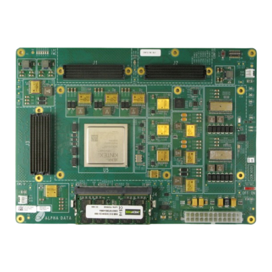
ADM-SDEV-BASE/XCKU060 User Manual V1.0 - 27th November 2018 Table Of Contents Introduction ............................1 Key Features ..........................2 References & Specifications ......................2 Environmental & Specifications ..................... 2 Installation ............................3 Software Installation ........................3 Hardware Installation ........................3 2.2.1 Handling Instructions ......................... - Page 4 Table 15 Config FMC Groups (J2) ........................18 Table 16 FMC+ Groups (J3) ........................... 18 List of Figures Figure 1 ADM-SDEV-BASE/XCKU060 Top View ..................... 1 Figure 2 ADM-SDEV-BASE/XCKU060 Block Diagram ..................4 Figure 3 LED Locations ........................... 6 Figure 4 JTAG Boundary Scan Chain ......................
-
Page 5: Introduction
V1.0 - 27th November 2018 1 Introduction The ADM-SDEV-BASE/XCKU060 shall be the base board at the core of the ADA-SDEV-KIT1 space FPGA development kit, enabling customers interested in space grade FPGAs to prototype their applications on a compatible XCKU060-1I device. -
Page 6: Key Features
ADM-SDEV-BASE/XCKU060 User Manual V1.0 - 27th November 2018 1.1 Key Features Key Features • Custom Form Factor • Modular design structure • Powered via an external power supply • Fitted with XCKU060-1FFVA1517I FPGA device as standard • PCB footprint compatible with QRKU060-CNA1509 (Contact factory for details) •... -
Page 7: Installation
The power dissipation of the board is highly dependent on the Target FPGA application. A power estimator spreadsheet is available on request from Alpha Data. This should be used in conjunction with Xilinx power estimation tools to determine the exact current requirements for each power rail. -
Page 8: Functional Description
Q227 Q226 XCKU060-FFVA1517-1-I FMC+ XQRKU060-CNA1509 Q126 Q127 Q225 Q128 Q224 JTAG QSPI FMC #2 Config Serial IO IPASS PCIe x1 Programmable 2x SATA System Clock SMA Clock Monitor Generator Figure 2 : ADM-SDEV-BASE/XCKU060 Block Diagram Page 4 Functional Description ad-ug-1360_v1_0.pdf... -
Page 9: Switch Definitions
ADM-SDEV-BASE/XCKU060 User Manual V1.0 - 27th November 2018 3.1.1 Switch Definitions There is a sliding switch situated on the bottom right corner of the board, plus a set of eight DIP switches and a push button switch placed on the top right corner of the board. Their functions are described in Switch Definitions. -
Page 10: Led Definitions
ADM-SDEV-BASE/XCKU060 User Manual V1.0 - 27th November 2018 3.1.2 LED Definitions The position and description of the board status LEDs are shown in Locations: D1 D2 D3 D4 D5 D6 Figure 3 : LED Locations Comp. Ref. Function ON State... -
Page 11: Jtag Interface
ADM-SDEV-BASE/XCKU060 User Manual V1.0 - 27th November 2018 3.2 JTAG Interface 3.2.1 On-board Interface A JTAG boundary scan chain can be accessed via a standard connector on the config FMC (J2). This allows the connection of the Xilinx JTAG cable for FPGA debug using the Xilinx toolchain. -
Page 12: Clocks
ADM-SDEV-BASE/XCKU060 User Manual V1.0 - 27th November 2018 3.3 Clocks The ADA-SDEV-BASE board provides a wide variety of clocking options. In addition to the and clocks routed from the FMC connectors, the board has 2 user-programmable clock generators. These clocks can be combined with the FPGA's internal PLLs to suit a wide variety of communication protocols. -
Page 13: Reference Clocks (Refclk400M And Fabric_Clk)
There are two programable clock sources that are forwarded throughout the FPGA. These clocks are programmable through the Alpha Data ADA-SDEV-BASE SDK. PROGCLK0 and PROGCLK1 are generated by a dedicated programmable clock generator IC and offer extremely high frequency resolutions (1ppm increments). -
Page 14: Module To Carrier Mgtref Clocks (Gbtclk_M2C)
ADM-SDEV-BASE/XCKU060 User Manual V1.0 - 27th November 2018 Signal Frequency FPGA Input IO Standard "P" pin "N" pin CLK1_M2C_0 Variable Bank 44 LVDS AM22 AN22 CLK1_M2C_1 Variable Bank 44 LVDS AM21 AN21 CLK2_M2C_0 Variable Bank 24 LVDS AM32 AN32 CLK2_M2C_1... -
Page 15: Configuration
ADM-SDEV-BASE/XCKU060 User Manual V1.0 - 27th November 2018 3.4 Configuration There are two main ways of configuring the FPGA on the ADM-SDEV-BASE: • From Flash memory on the config FMC board, at power-on, as described in Section 3.4.1 • Using a Xilinx Platform JTAG cable connected to the programming header on the config FMC board Section 3.4.2... -
Page 16: Configuration Via Jtag
ADM-SDEV-BASE/XCKU060 User Manual V1.0 - 27th November 2018 • -loadbit "up 0x0000000 <directory/to/file/filename.bit>" (0th location) • -loadbit "up 0x2000000 <directory/to/file/filename.bit>" (1st location, optional) Program with vivado hardware manager with these settings (see xapp1233): • SPI part: mt25qu256-spi-x1_x2_x4_x8 • State of non-config mem I/O pins: Pull-none •... -
Page 17: Health Monitoring
ADM-SDEV-BASE/XCKU060 User Manual V1.0 - 27th November 2018 3.5 Health Monitoring The ADA-SDEV-BASE has the ability to monitor temperature and voltage to maintain a check on the operation of the board. The monitoring is implemented using the Atmel AVR microcontroller. -
Page 18: Automatic Temperature Monitoring
ADM-SDEV-BASE/XCKU060 User Manual V1.0 - 27th November 2018 3.5.1 Automatic Temperature Monitoring At power-up, the control logic sets the temperature limits and resets the temperature sensor's over-temperature interrupt. The temperature limits are shown below : FPGA Board Industrial -40 degC... -
Page 19: Fpga
ADM-SDEV-BASE/XCKU060 User Manual V1.0 - 27th November 2018 3.6 FPGA 3.6.1 I/O Bank Voltages The FPGA IO is arranged in banks, each with their own supply pins. The bank numbers, their voltage and function are shown in Target FPGA IO Banks. -
Page 20: Figure 7 Mgt Links
ADM-SDEV-BASE/XCKU060 User Manual V1.0 - 27th November 2018 Kintex Ultrascale Config FMC2_DP(3:0) MGT225 (J2) FMC1_DP(3:0) MGT224 (J1) MGT226 FMC3_DP(3:0) FMC3_DP(7:4) MGT227 FMC3_DP(11:8) MGT228 FMC+ (J3) FMC3_DP(15:12) MGT126 FMC3_DP(19:16) MGT127 FMC3_DP(23:20) MGT128 Figure 7 : MGT Links Page 16 Functional Description... -
Page 21: Memory Interfaces
ADM-SDEV-BASE/XCKU060 User Manual V1.0 - 27th November 2018 3.7 Memory Interfaces The ADA-SDEV-BASE has a single SODIMM socket, capable of supporting a DDR3 (with ECC) SODIMM module, spread across 3 FPGA IO banks (66/67/68). The memory banks are arranged for compatibility with the Xilinx Memory Interface Generator (MIG). -
Page 22: Fmc Interfaces
ADM-SDEV-BASE/XCKU060 User Manual V1.0 - 27th November 2018 3.8 FMC Interfaces The ADA-SDEV-BASE board has 3 FMC sockets, J1, J2 and J3. Their interfaces are described below. 3.8.1 Low Pin Count (LPC) FMC, J1 Connector J1 is for general purpose IO. - Page 23 ADM-SDEV-BASE/XCKU060 User Manual V1.0 - 27th November 2018 FPGA Group Name Function Bank FMC3_HB(16:7) 10 diff. Pairs / 20 single-ended FMC3_HB(21:18) 4 diff. Pairs / 8 single-ended FMC3_HB_0 FMC3_HB_CC (0) Regional Clock / GPIO pair / 2 single-ended FMC3_HB_CC (6)
- Page 24 ADM-SDEV-BASE/XCKU060 User Manual V1.0 - 27th November 2018 Revision History Date Revision Nature of Change Initial Draft 12 Sep 2018 Updated after review 21 Sep 2018 First Release 27 Nov 2018 Address: 4 West Silvermills Lane Address: 611 Corporate Circle, Suite H...
Need help?
Do you have a question about the ADM-SDEV-BASE/XCKU060 and is the answer not in the manual?
Questions and answers